Ensuring Superior Solderability: The Critical Role of Testing in Reliable PCB Production
16 min
- What Solderability Testing Is and Why It Matters
- Common Solderability Test Methods and Standards
- Factors That Influence Solderability Performance
- How to Interpret Solderability Test Results
- Design and Process Improvements to Enhance Solderability
- JLCPCB's Professional Approach to Solderability Assurance
- FAQ about Quality & Reliability Testing
- Conclusion
Key Takeaways
- Core Purpose: Verifies solder wetting before assembly to prevent yield drops and joint failures.
- Destructive Test: Per J-STD-002, tested components and coupons cannot be reused in production.
- Pass Standards: Requires 95 percent solder coverage on leads and 80 percent on exposed thermal pads.
- Key Defects: Catches non-wetting (exposed metal), dewetting (solder pulling back), and black pad on ENIG.
- DFM Prevention: Use thermal relief, keep silkscreen off pads, and select the right surface finish for shelf life.
A solderability test answers one question before you commit a single reel to the line: Will molten solder actually stick to this surface? Skip it, and you find the answer during reflow, when a tray of boards comes out with open joints and tombstoned parts.
In this guide, you will learn:
- What a solderability test measures, and why wetting fails
- Dip-and-look, wetting balance, solder float, and reflow simulation, compared
- Real J-STD-002 and J-STD-003 parameters: temperatures, dwell times, aging
- How to read a wetting curve and a 95% coverage call
- Root causes behind non-wetting, dewetting, and black pad
- Storage and design choices that protect solderability
What Solderability Testing Is and Why It Matters
Definition and Purpose in PCB Manufacturing
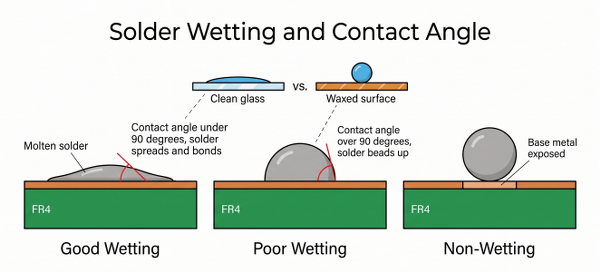
A solderability test measures how well a metal surface can be wetted by molten solder. J-STD-002 defines solderability exactly that way, and defines wetting as the formation of a smooth, unbroken, adherent film of solder on the base metal.
Take an example, of water on glass: On a clean pane, it spreads into a thin sheet. On a waxed car hood, it pulls into beads and rolls off. Solder does the same, and the angle it makes with the surface is the giveaway. Below 90 degrees, it spreads and bonds. Above 90 degrees, it beads up and walks away. The point is not to prove solder works. It is to prove that time has not ruined the surface. A board that soldered perfectly in March may not solder in November.
Note: Solderability testing is destructive. J-STD-002 clause 1.7 says a tested component shall not be reused for functional evaluation, so budget sacrificial parts and coupons into the build.
The Link Between Solderability and Assembly Quality
Poor solderability rarely shows up as one obvious defect. It shows up as a yield number that quietly drops. A batch of 0402 resistors with oxidized terminations will tombstone, skip, and leave head-in-pillow joints across the panel, and none of that looks like a storage problem on the optical inspection report. The cost lands downstream. Reworking a 0.5 mm (20 mil) pitch LQFP-48 package, such as an STM32F103C8T6, costs far more in labor than the part itself, and every rework cycle adds thermal stress the board never budgeted for. Worse, marginal joints pass the electrical test and fail months later in the field, because the bond underneath was always thin.
Common Solderability Test Methods and Standards
Dip-and-Look, Wetting Balance, and Other Techniques
Five methods matter in production, and they split into two families. Visual methods dip the sample and let a person judge the coating. Force methods dip it and let a load cell measure the pull.
| Method | What Happens | Best Used For |
|---|---|---|
| Dip-and-Look (J-STD-002 Test A/B) | Flux the lead, dip in a solder pot, and inspect at 10X | Incoming inspection, pass/fail on coverage |
| Wetting Balance (Test E/F) | Sample hangs from a transducer, dips 0.4 mm (16 mil) in | Comparing suppliers, root cause work |
| Reflow Simulation (Test S) | Paste printed on ceramic, part placed, panel reflowed | Surface-mount parts, matching your own oven |
| Solder Float (J-STD-003) | Coupon floats on the bath, solder wicks up the holes | Through-hole barrel fill, wave-solder boards |
| Edge Dip (J-STD-003) | Coupon edge fluxed and dipped to a set depth | Bare-board finish qualification |
The wetting balance does not look at the joint. It weighs it, logging vertical force every few milliseconds. The curve has three landmarks:
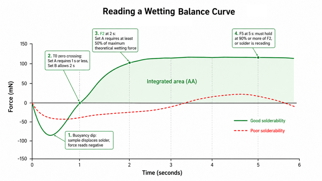
- The dip. Force goes negative first because you pushed a solid into a liquid. The instrument subtracts that buoyancy using the solder density, roughly 8020 kg per cubic meter for Sn63Pb37 at 245 degrees C.
- The zero crossing (T0). The moment wetting cancels the buoyancy. Set A in J-STD-002D requires it within 1 second, Set B within 2 seconds.
- The plateau (F2 and F5). Set A wants the force at 2 seconds to reach at least 50% of the maximum theoretical wetting force. Both sets require the force at 5 seconds to be at least 90% of the 2-second value.
That last one is the one that people do not see. If F5 is below 90% of F2, the solder is melting back, and you have a real-time demonstration of dewetting.
Key Industry Standards (IPC, J-STD, MIL-STD)
The standard you quote will be based on what you are testing. There are documents for components and boards, and the most frequent mistake in suppliers' documentation is the mix-up between components and boards.
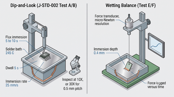
- J-STD-002 covers component leads, terminations, lugs, terminals, and wires: Revision D defines Tests A, B, C, D, and S for tin-lead, and A1, B1, C1, and S1 for lead-free. The bath sits at 245 ± 5 °C, dwell is 5 seconds with a tolerance of ±0.5 seconds, and the immersion rate is 25 ± 6 mm/s (0.98 ± 0.24 in/s).
- J-STD-003 covers bare boards: surface conductors, attachment lands, and plated-through holes. Revision D, issued October 2022, names its methods Edge Dip, Wave Solder, Surface Mount Simulation, Solder Float, and Wetting Balance. Its tin-lead bath runs cooler at 235 degrees C, while SAC305 lead-free testing runs at 255 degrees C in both documents.
- IPC-TM-650 Method 2.4.14: "Solderability of Metallic Surfaces," is the legacy method behind much of this: a 232 plus or minus 6 degrees C pot, 25% rosin by weight in 99% isopropyl alcohol, immersion at about 1.3 cm per second (0.5 inch per second), a 2-second dwell, and inspection at 10X.
- MIL-STD-202G Method 208H is the military route: It defers to J-STD-002 for procedure, then overrides the aging: 8 hours plus or minus 15 minutes of steam conditioning for most components, and 1 hour plus or minus 5 minutes for stranded wire.
Now, the secret that most engineers keep. Preconditioning is always described as "8 hours of steam aging." For J-STD-002D, which is Condition Category C, all four steam categories (1, 4, 8, 16 hours) are marked as Optional Legacy. The default is now Category E: a dry bake at 155 degrees C for 4 hours and 15 minutes.
The 8-hour steam requirement is still required by MIL-STD-202G Method 208H. Work in the aerospace and defense field gets heated. The dry bake is for commercial work.
Factors That Influence Solderability Performance
Surface Finish Type, Storage Conditions, and Aging Effects
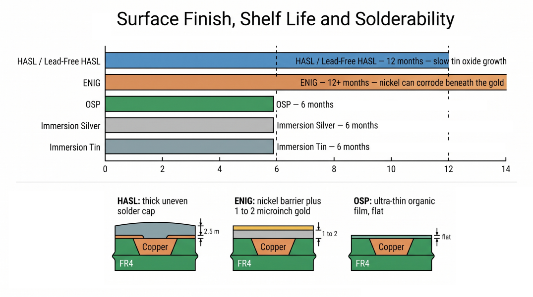
The finish is the thing being tested. Every finish is a temporary barrier keeping oxygen off the copper, and every barrier has a clock on it.
| Surface Finish | Typical Shelf Life | How It Degrades | Choose It When |
|---|---|---|---|
| HASL and lead-free HASL | About 12 months | Slow tin oxide growth, coating stays thick | Through-hole, hand-soldered boards |
| ENIG | 12 months or more | Gold is fine, nickel can corrode underneath | Fine-pitch BGA and QFN, multiple reflows |
| OSP | Around 6 months | Organic film thins with every heat cycle | Flat, low-cost boards, single reflow |
| Immersion Silver | Around 6 months | Tarnishes with sulfur and humidity | RF boards needing low loss and flatness |
| Immersion Tin | Around 6 months | Copper-tin intermetallic eats the free tin | Press-fit connectors, fine-pitch work |
The rule of thumb is that the thicker the metallic coating, the longer it will last, and the finer the finish, the shorter its shelf life, since fine-pitch assembly requires planarity. For a detailed explanation, refer to the sections on selecting the appropriate surface finish and the HASL vs. ENIG comparison. The rest of the harm is done during storage. Store boards and reels sealed in moisture-barrier bags at 15-30 °C and 40-65% RH, containing a desiccant and a humidity indicator card.
Material and Process Variables Affecting Test Results
Failure isn't the part. It's the test. A drifting lab fails good and passes bad for one of three reasons.
The bath: J-STD-002 calls for a solder bath analysis or change every 30 operating days, where an operating day is defined as an eight-hour period of molten solder. Copper is limited to 0.300% by weight in tin-lead alloys, and the total of copper, gold, cadmium, zinc, and aluminum combined is limited to 0.4%. Lead from thousands of dips will cause the bath to become sluggish and grainy, with false-fail joints.
The flux: Test fluxes must be covered during breaks and discarded after eight hours. Isopropyl alcohol evaporates through a shift, and the concentrated flux left behind is more aggressive than the standard specifies.
The magnification: Parts are inspected at 10X. At 0.5 mm (20 mil) pitch or less, inspection rises to 30X, with referee inspection at 30X, or 70X for fine-pitch leaded parts. An LQFP checked at 10X hides pinholes that the standard expects you to find.
If you change the bath, the flux, or the magnification, you have changed the result. Fix the lab before you blame the supplier.
How to Interpret Solderability Test Results
Pass/Fail Criteria and Common Failure Modes
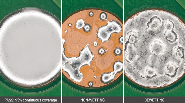
For each lead/tail/termination, J-STD-002D requires that the solder be free of defects and present at 95% of the critical area. This is per lead, not averaged; thus, if one lead fails on a 48-pin package, the package fails.
| Criterion | Threshold | What Failing It Tells You |
|---|---|---|
| Lead and termination coverage | 95% minimum, continuous | The finish has oxidized or is contaminated |
| Exposed pad coverage (QFN thermal pads) | 80% minimum | Large flat areas outgassing or heat-starved |
| Resistance to dissolution (Test D) | Max 5% base metal exposed | Metallization is leaching into the solder |
| Plated-through hole vertical fill | 75% Class 3, 50% Class 2 | Barrel wall not wetting, or hole heat-starved |
| Wrapped wire fillet (Test C) | 95% of the fillet length tangent | The terminal is oxidized or plated too thin |
That is a hierarchy of forgiveness: small contacts get a hard 95%, thermal pads get 80% because voiding is unavoidable on a large flat area, and barrels get a fill percentage because you only see the outside.
Three defect types matter, and the standard defines each precisely:
- Non-wetting is partial adherence. Solder stuck in patches, leaving base metal exposed. Usually, it is oxide or organic contamination.
- Dewetting is worse and more deceptive. Solder wet the surface, then pulled back into irregular mounds. Base metal stays covered, so it passes a glance, but the coating underneath dissolved into the solder.
- Pinholes penetrate straight through the coating, pointing to outgassing from the base material or a plating bath.
Root Cause Analysis for Poor Solderability
A batch of Wi-Fi router boards came off reflow with open joints under the shield frame, and the profile took the blame. Cross-sectioning told a different story: the pads had wet, then fractured, and were cleaned off at the nickel interface. The boards were an eight-month-old ENIG lot, and the fracture surface was dark and mud-cracked. The gold bath had over-attacked the nickel-phosphorus layer during plating, leaving corrosion on the gold, which then hid. That is a black pad.
Mistake 1: Blaming reflow when the parts failed at incoming.
A profile change is cheap to try, so it gets tried first, and each attempt burns a panel. To fix this: run a dip-and-look on parts from the same reel before you touch the oven.
Mistake 2: Testing without preconditioning and calling it a pass.
Fresh, unaged parts are almost always wet. To fix this: precondition to the agreed category, either the 155 degrees C dry bake default or the 8-hour steam your customer specifies, and record which you used.
Mistake 3: Reading a wetting curve without buoyancy correction.
An uncorrected curve makes a poor surface look like it crossed zero early. To fix this, enter the true immersed volume, width times thickness times immersion depth, so the software subtracts buoyancy before reporting T0.
Mistake 4: Re-testing the same coupon after a fail.
The first dip already tinned it, so the second test measures the solder you just applied. To fix this: pull a fresh coupon from the same panel.
Design and Process Improvements to Enhance Solderability
DFM Guidelines for Better Solderability
Some solderability failures are designed in. The finish is fine, the parts are fine, and the layout still starves the joint of heat or blocks the pad. The biggest offender is the copper connection. A pad tied straight into a large ground plane acts as a heatsink, so it never reaches wetting temperature while its neighbor does, and the part tombstones. Thermal relief spokes solve it, and the copper pour guide covers the trade-off.
Rules worth building into your design rule checks:
- Thermal relief on plane connected through-hole pads: The 0.25 to 0.5 mm (10-20 mil) wide four-spoke configuration is acceptable for most signal pins.
- Do not put solder mask on the pad: The plotter has 0.05 mm (2 mil) on each side of the mask to miss without exposing copper.
- Do not wear a mask that is lower than the mask dam: The dam will not print, and openings merge together below ~0.1 mm (4 mil) between pads.
- Maintain a reasonable aspect ratio for plated-holes: If the board thickness/drill diameter is above 8/1, barrel plating will be more difficult, and the barrel will wet unevenly if the plating is uneven.
- Avoid putting silkscreen on the pads and on the holes: Barrels that will not fill are a common occurrence with ink on copper blocks wetting completely. Clearances are covered in the PCB silkscreen guide.
Surface Finish Selection and Storage Best Practices
Pick the finish for the assembly process, not the datasheet. It comes down to how flat the surface must be and how many times it will see reflow.
- Fine-pitch BGA, QFN, or multiple reflows: ENIG. Flat, survives repeated heating, holds a year or more.
- Single reflow, cost-driven board: OSP is flat and cheap, but assembly within six months and in one pass.
- Through-hole heavy or hand-assembled: HASL is the most forgiving, though its uneven surface rules out the finest pitches.
- RF and high-frequency: immersion silver, stored away from sulfur-bearing air.
- Gold wire bonding or highest reliability: ENEPIG adds a palladium barrier between nickel and gold, removing the black pad mechanism entirely.
The storage discipline is boring, and it works: sealed bags, fresh desiccant, strict first-in-first-out, opening date on the bag.
JLCPCB's Professional Approach to Solderability Assurance
Rigorous In-Process and Final Solderability Testing
Solderability cannot be inspected at the end; it must be controlled at each step that involves copper. This implies not only observing the board it creates, but also monitoring the chemistry that deposits the finish.
It includes bath concentration and pH regulation on the plating lines, controlled dwell in each chemical stage, deionized water rinsing to prevent ionic residue from the copper, optical inspection, and full electrical test before packing. Boards are then put into sealed bags with desiccant, and the shelf-life clock begins as late as possible.
Advanced Process Control for Consistent Surface Finish Quality
JLCPCB offers HASL, lead-free HASL, ENIG with a choice of 1 or 2 microinch gold thickness, OSP, immersion silver, and immersion tin. One capability decision is really a solderability decision. HASL cannot be leveled flat enough for dense fine-pitch work, so it is excluded from 6-layer and higher stackups in favor of flatter finishes such as OSP and ENIG. That is the difference between a BGA that wets evenly across every ball and one that does not.
First-pass yield is the point at which solderability appears as a number in a report. Every joint that doesnot gett wet becomes a rework cycle, and every rework cycle adds heat the board was never designed to absorb. The reliability side is quieter and matters more. A properly wetted joint forms a thin, even intermetallic layer that survives thermal cycling for years. A marginal joint forms a thick or patchy one that cracks under the same load.
FAQ about Quality & Reliability Testing
Q: What is the difference between J-STD-002 and J-STD-003?
J-STD-002 tests components: leads, terminations, lugs, terminals, and wires. J-STD-003 tests bare printed boards and uses a cooler tin-lead bath at 235 degrees C, against 245 degrees C for components.
Q: How long do PCBs stay solderable in storage?
It depends on the finish. HASL and ENIG typically hold about 12 months or more, while OSP, immersion silver, and immersion tin are usually rated around 6 months, assuming sealed bags with desiccant at 15 to 30 degrees C.
Q: Can I bake old boards to restore solderability?
No. Baking removes absorbed moisture, a different problem. It does nothing to copper oxide, and it thins an OSP coating, so a bake can leave an OSP board worse than before.
Q:What solderability test equipment do I actually need?
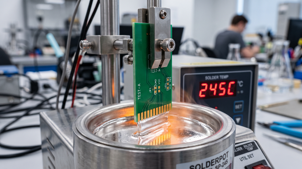
Dip-and-look needs a thermostatically controlled solder pot, a mechanical dipper capable of dipping at 25 ± 6 mm/s, a stopwatch, and a 10X microscope with a reticle. A wetting balance adds a micro-Newton force transducer and is usually outsourced to a lab.
Q: Why did my board pass its solderability test but still fail at reflow?
The test qualifies the surface, not the design or the profile. Pads tied to planes without thermal relief, pads blocked by silkscreen, or an underpowered profile all starve a joint of heat, even on a solderable finish.
Conclusion
A solderability test is really a test of time. Almost any finish solders well on day one, and the discipline exists to determine whether that remains true after six months in a warehouse. A dip-and-look at 10X or a full wetting balance curve both measure how much of that original readiness survived.
So, make the decision earlier. Choose the finish for when the board will actually be assembled, store it as though the clock is running, and design the pads so heat reaches them. Get those three right, and the test stops being about discovering a problem.

Keep Learning
Why PCB Test Coupons Are Critical for Reliable Board Manufacturing
Key Takeaways Sacrificial Testing: Coupons allow destructive tests without harming active boards. True Process Mirror: They match the exact stackup and density to reflect panel quality. Clean Measurements: Straight lines enable precise TDR impedance and via inspection. Quality Shield: Coupon failures isolate flawed panels before shipping. A PCB test coupon is the one piece of your order that is intentionally destroyed. It rides in the panel border beside your boards, so it sees every drill, plating, a......
How to Master PCB Impedance Testing for High-Speed Designs
Key Takeaways Verification via TDR: Impedance testing uses Time-Domain Reflectometry (TDR) on test coupons to verify high-speed traces. Real-World Factors: Actual impedance is shifted by manufacturing variables, including trace undercut, solder mask, and pressed dielectric thickness. Design-to-Fab Loop: Use the manufacturer's exact stackup Dk values for layout and TDR reports to refine revisions within $\pm 10\%$ tolerance. An impedance test can be the difference between a USB 3.0 link that works reli......
Guardians of Quality: A Complete Walkthrough of PCB Inspection Standards
Key Takeaways Layered Defense: Combining AOI, AXI, ICT, and FCT covers all inspection blind spots. Paste Printing: Solder paste causes up to 60% of defects, making early checks vital. IPC Standards: IPC Class 3 tightens BGA void limits from 25% to 10%, raising costs. Thermal Balance: Equal layout heating balances reflow pull to prevent tombstoning. Design Control: Clear test pads and visible polarity marks ensure reliable automated checks. PCB inspection is not one check performed at the end of produc......
Ensuring Superior Solderability: The Critical Role of Testing in Reliable PCB Production
Key Takeaways Core Purpose: Verifies solder wetting before assembly to prevent yield drops and joint failures. Destructive Test: Per J-STD-002, tested components and coupons cannot be reused in production. Pass Standards: Requires 95 percent solder coverage on leads and 80 percent on exposed thermal pads. Key Defects: Catches non-wetting (exposed metal), dewetting (solder pulling back), and black pad on ENIG. DFM Prevention: Use thermal relief, keep silkscreen off pads, and select the right surface fi......
Solder Joint Inspection in PCB Manufacturing : A Complete Guide to Catching Defects Early
Key Takeaways Solder Joint Inspection is critical in modern PCB manufacturing to catch defects early and ensure product reliability. By combining Solder Paste Inspection (SPI), 3D AOI for visible joints, and X-ray for hidden BGA/QFN issues, manufacturers can effectively detect common defects such as bridging, cold joints, tombstoning, and head-in-pillow. Following IPC-A-610 standards with a layered inspection strategy significantly reduces field failures while improving first-pass yield. JLCPCB’s prof......
3D AOI Inspection Explained : How It Catches Defects That 2D Systems Miss
Key Takeaways 3D AOI Inspection has become essential in modern PCB assembly by using advanced height and volume measurement to detect critical solder defects that traditional 2D AOI systems routinely miss, such as lifted leads, insufficient solder, head-in-pillow, and component coplanarity issues. By delivering precise 3D data through structured light or Moire technology, it significantly reduces false calls, improves first-pass yield, and ensures long-term reliability according to IPC-A-610 standards......