How PCB Thermal Cycling Tests Reveal Manufacturing Reliability
14 min
- What Is a Thermal Cycle Test for PCBs?
- How PCB Thermal Cycling Tests Are Performed
- PCB Thermal Cycling Failures and Failure Analysis
- How Professional PCB Manufacturing Improves Thermal Reliability
- FAQs About PCB Thermal Cycling Tests
- Conclusion
Key Takeaways
- Exposes Hidden Faults: Thermal expansion opens tiny cracks, catching via failures that room tests miss.
- Expansion Mismatch Stress: Heat differences weaken vias and solder joints over time.
- Standardized Testing: Follows IPC and JESD rules, failing when resistance increases.
- Process Prevention: High Tg materials, thick copper, and filled vias boost board life.
- Destructive Test: Consumes board life, so tested samples must be scrapped.
A PCB thermal cycling test can detect faults that a room-temperature electrical test cannot. A cracked via barrel will usually close up when the board cools down. The crack may open when the laminate is hot and swollen, but no one is probing it then.
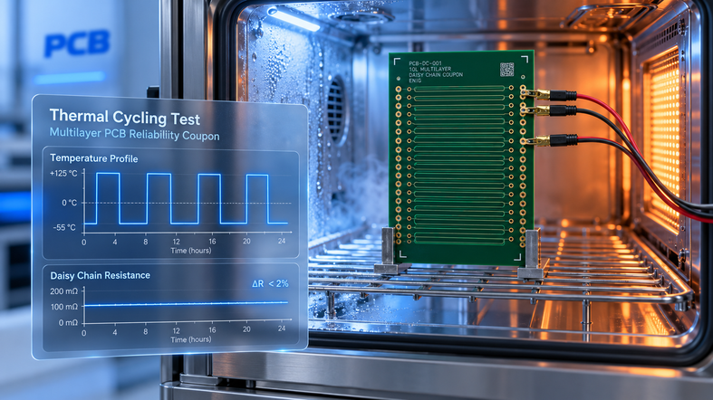
Figure 1: PCB coupon in a thermal cycling chamber with its resistance plotted live
This is due to a mismatch in expansion: Copper expands by approximately 17 ppm/°C, whereas the epoxy surrounding a plated hole expands by more than double this amount through its thickness. With each heating/cooling cycle, the copper barrel is stretched and allowed to cool, similar to bending a paper clip back and forth. This guide will describe the purpose of the thermal cycle test and how it is different from other reliability tests. It addresses the parameters and methods employed by labs, as well as the failure modes they reveal.
What Is a Thermal Cycle Test for PCBs?
A Thermal Cycle Test is a method of cycling a board or coupon between cold and hot states (or vice versa) and comparing the interconnect resistance. It's a measure of fatigue, which means it's not just one pass.
Why Thermal Cycling Matters for PCB Reliability
Regardless of whether you intend to thermally cycle a working board, you are doing so. Power-up, load change, and day/night temperature swings cause differential heating of the laminate and copper, causing the interconnects to flex slightly with each change. Damage is additive - that is, a via can open after months of service without any one event occurring. That is why the reliability question cannot be answered by fabrication testing.
At room temperature, a flying probe tests continuity by pressing a fine barrel crack together and verifying it remains conductive. Thermal cycling places the same stresses on the structure and under the conditions that opened them; latent defects are observed in the laboratory. Fatigue life also declines sharply as the temperature range increases, a behavior modeled with Coffin-Manson-type equations. Thus, years in the field are condensed into weeks of mild cycling under a wide test range.
Thermal Cycling vs. Other PCB Reliability Tests
Thermal cycling is a measure of fatigue, whereas most other thermal tests assess the survival of a single extreme event. The thermal stress test in IPC-TM-650 2.6.8 (Revision E) is a method in which the sample is placed on molten solder at 288 °C for 10 seconds. It does not indicate how many cycles plated holes will endure, but whether they pass a soldering shock.
A reflow simulation according to IPC-TM-650 2.6.27 (Revision B) simulates the heat of convection reflow assembly. The humidity and vibration tests are used for testing moisture and mechanical loading at constant temperature. None of them reproduces their expansion and interconnections each time the product is turned on. That's why IPC-TM-650 2.6.7.2 includes a reflow simulation before cycling: Assembly and service damage are cumulative.
How PCB Thermal Cycling Tests Are Performed
Each thermal cycling test is based on four options: temperature extremes, rate of change, dwell at each extreme, and failure criterion. Then, the method and the monitoring determine the degree of fidelity of those choices with the copper.
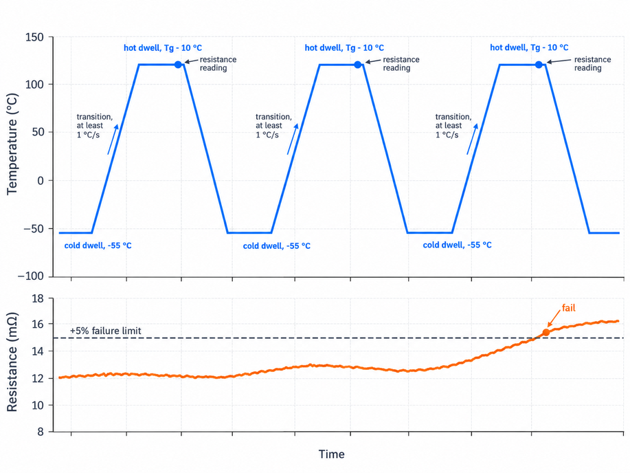
Figure 2: Thermal cycling profile with ramps, dwells, and resistance readings
Common Test Parameters
The upper limit of the hot extreme is set by the laminate's glass transition temperature (Tg), since the failure mechanism differs above Tg. IPC-TM-650 2.6.7.2 (Revision C, 2020) has therefore maintained the hot end of the default quality conformance test at a temperature 10 °C lower than Tg. It is set to −55 °C as the default cold extreme.
| Test Profile | Temperature Range | Cycles and Transition | Failure Criterion | What It Tells You |
|---|---|---|---|---|
| IPC-TM-650 2.6.7.2C, quality conformance | −55 °C to the lowest of Tg − 10 °C, reflow peak − 25 °C, or 210 °C | 100 cycles, at least 1 °C per second | Over 5% resistance change | Whether a lot of plated holes are sound |
| IPC-TM-650 2.6.26A IST, default | Room temperature to 150 °C | 250 cycles, DC heating | 10% resistance rise | Via fatigue in about a day |
| IPC-9701 TC1 (current Revision B, 2022) | 0 °C to 100 °C | 10-minute dwells | Continuous monitoring per IPC-9701B Table 4-2 | Reference solder joint fatigue life |
| JESD22-A104 Condition G | −40 °C to +125 °C | Set by the qualification plan | Set by the referencing specification | Interconnect robustness in harsh service |
Bare board tests cap the hot extreme near Tg and fail a net at a 5-10% change in resistance.
Methods of PCB Thermal Cycling Test
There are two families of PCB thermal cycling methods, depending on the heat source. This is because in the case of chambers, the entire sample is heated from the outside, whereas in current-induced testing, the copper is heated from the inside.
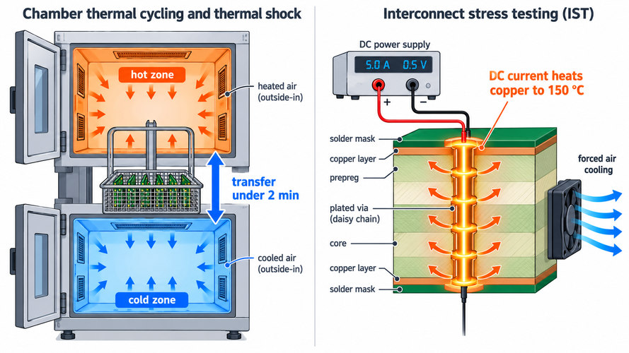
Figure 3: Thermal cycling compared with current-induced interconnect stress testing
- Chamber thermal cycling and thermal shock: air chambers heat and cool the entire sample, either in a single chamber or by moving the sample between chambers.
- Interconnect stress testing (IST): Pulses of DC through the coupon's own daisy chain heat the interconnects, which are then cooled by fans.
Chamber testing is the reference method because it mimics how the material would heat up in the environment. According to IPC-TM-650 2.6.7.2C, a thermal cycle is the temperature change rate of less than 1 °C per second on the sample surface. The thermal shock rate is obtained in less than 2 minutes, with samples moved between hot and cold chambers using a dual-chamber system.
Monitoring PCB Performance During Testing
Monitoring causes all the interconnects to be replaced by a single long resistance. A test coupon is a daisy chain of hundreds of vias or solder joints for testing. Thus, a single crack anywhere increases the resistance of the entire net, and a four-wire measurement eliminates lead resistance.
A barrel crack will only occur when the laminate is hot and expanded. According to IPC-TM-650 2.6.7.2C, resistance is recorded towards the end of each hot dwell as follows:
- Bake the coupon for a minimum of 6 hours at 105-125 °C to remove moisture.
- Conduct 6 reflow simulations following IPC-TM-650 2.6.27 and take note of the ambient resistance.
- The 1RM for the first cycle will be the reference resistance.
- Write down the maximum resistance at the end of each subsequent hot dwell.
- Reject the net if it exceeds the reference by more than 5%, unless otherwise agreed by the buyer.
A solder joint test must be performed quickly, as the crack can open for a few microseconds before closing again. Thus, it is recommended for continuous monitoring by IPC-9701B, and published TC1 studies utilize an event detector to alert of any observed spike to 1,000 Ω or greater.
PCB Thermal Cycling Failures and Failure Analysis
Thermal cycling failure occurs at the junction between materials of different expansion rates. Thermal cycle test failure analysis also pinpoints the crack location and can trace it back to the material or process step that created it.
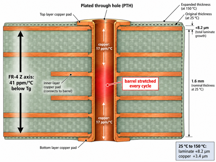
Figure 4: CTE mismatch stretching a plated through-hole barrel
Thermal Expansion and CTE Mismatch
CTE, or the coefficient of thermal expansion, is a material's rate of growth per degree (parts per million). Since the glass weave doesn't constrain FR-4 in the in-plane directions, it expands similarly to copper in X and Y, while there is no constraint through the thickness. Thus, the Z-axis CTE is higher and experiences another step over the glass transition temperature.
| Material | CTE (ppm/°C) | What It Means for Your Board |
|---|---|---|
| Copper (plating and foil) | 17 | The barrel cannot follow the resin in Z |
| FR-4, X and Y axes | About 13 to 17 | Planes and traces stay bonded in the plane |
| Shengyi S1000-2M, Z axis below Tg (typical) | 41 | The normal working strain on a via |
| Shengyi S1000-2M, Z axis above Tg (typical) | 208 | Why hot extremes stay below Tg |
| Alumina ceramic (chip resistor body, 96%) | About 8 or fewer | The board outgrows the part and shears its joints |
The mismatch turns into strain quickly. Heat a 1.6 mm (63 mil) S1000-2M board from 25 °C to 150 °C, and its thickness increases by about 8.2 µm (0.32 mil). A free copper barrel would grow only 3.4 µm (0.13 mil), so the difference on every cycle stretches the barrel.
Common Failure Modes in Solder Joints and Vias
There are two families of thermal cycling failures, depending on the location of the strain concentration. Vias fail in their copper, and solder joints fail in the solder or in the laminate underneath the pad.
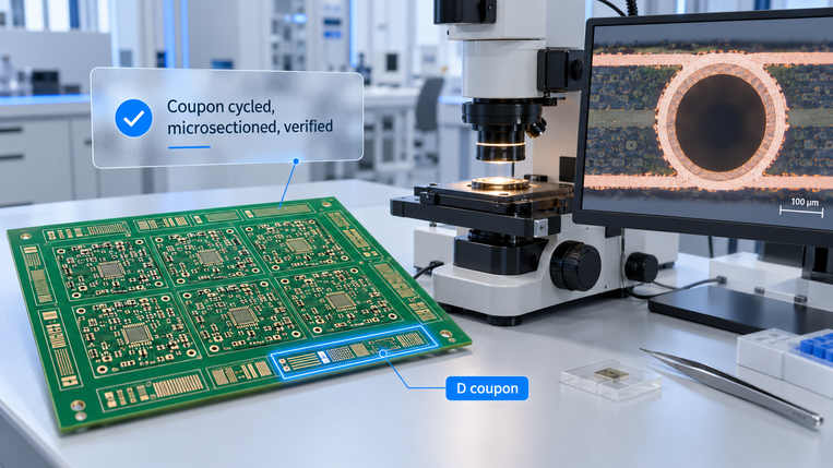
Figure 5: Microsections of a barrel crack, a knee crack, and an inner-layer separation
- Via and plated-hole cracks: barrel cracks, knee cracks at surface pad, and separation at inner-layer or microvia target pads.
- Solder-joint fatigue: cracks in the soldered joint close to the component terminal, with cratering of the solder pad in the laminate below.
Via cracks are created along the Z-axis stretch. Typically, the crack occurs near the middle of the hole where the plating is the thinnest. The knee crack begins where the barrel bends to the surface pad. Inner-layer and target pad separations are the most difficult to detect because they often conduct at room temperature.
Connecting Test Failures to Manufacturing Processes
Failure analysis identifies the failed net and microsections it, grinding away through the failed via or joint. The crack position lies between the design and process problems, since each manufacturing step has its own weaknesses, and it is predictable. That mapping is based on a PCB cross-section analysis.
| Failure Signature | Likely Process Cause | What to Check or Specify |
|---|---|---|
| Crack at mid-barrel | Thin plating deep in a high aspect ratio hole | Hole-wall copper against the IPC-6012 class limit |
| Knee crack at the surface pad | Thin surface copper or poor plating wrap | Wrap plating and surface copper thickness |
| Barrel separated from an inner-layer pad | Drill smear left by incomplete desmear | Desmear control and the inner-layer bond |
| Microvia target pad separation | Laser drilling residue or weak plating adhesion | A coupon for each microvia stack |
| Resin cracks or delamination near holes | Moisture or under-cured lamination | Baking before assembly, laminate Td and T260 |
| Early solder joint cracks | Voids, thin joints, or a large component mismatch | Voiding by X-ray and component choice |
How Professional PCB Manufacturing Improves Thermal Reliability
The thermal cycling life is largely determined before the first thermal cycle. It is determined by the laminate, the stackup, and the consistency of drilling and plating, and a fabricator can enhance reliability by controlling those factors.
Material and Stackup Control
The strain to be carried by each via is set by the material choice. The higher the Tg, the more of the board's working range is maintained on the lower Z-axis CTE. The high decomposition temperature (Td) ensures protection of the resin even after repeated reflowing without lead. Compare the Z-axis CTE and T260 delamination time, and Tg as discussed in "How to select the Tg of a PCB.”
From the numbers, the datasheet for Shengyi S1000-2M lists a typical Tg of 180 °C, as measured by DSC, and a Td of 355 °C. JLCPCB's capabilities page features Grade A laminates from Nan Ya, KB, and Shengyi. It is an HDI based on Nan Ya NP-175F or S1000-2M TG170. Asymmetry is a factor in stackup control because it introduces bending to expansion. When the board warps during heating due to an unbalanced copper layer or an unbalanced (non-uniform) dielectric layer, it further stresses the BGA corner joints.
Process Control for Vias and Interconnects
The most obvious factor in determining barrel life is plating thickness: the thicker the copper, the more spread over a larger number of metals. A minimum average hole-wall copper of 20 µm (0.8 mil) is required for IPC-6012F (Revision F, 2023), Class 2. Class 3 increases it to 25 µm (1.0 mil), and the IPC-6012 performance classes indicate which one is required for your service.
The question of the bond of copper depends on the method of drilling and hole preparation. A dull drill will put resin all over the inner-layer copper. It remains on the barrel as a plate on resin, rather than as bare copper, unless removed by desmear. That interface survives the electrical test but separates during cycling (inner-layer failure, as shown above). The final lever is via structure. Vias are filled and capped to eliminate trapped air and provide pad support. On JLCPCB's capabilities page, they mention that they use epoxy-filled and capped vias as the default model for boards with 6 or more layers.
Reliability Testing and Quality Verification
Thermal reliability is verified on coupons by a fabricator, not your boards. Two nets per coupon; D coupons have the largest plated holes, the smallest vias, and all blind, buried & filled via structures. Since all coupons in a panel are drilled and plated simultaneously, a surviving coupon can represent the nearby product.
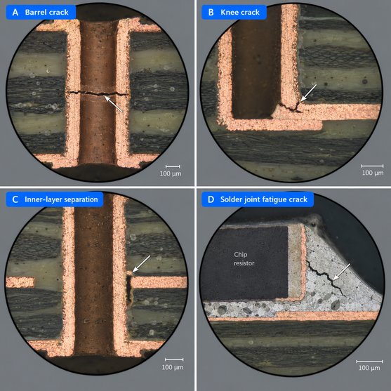
Figure 6: Production panel with D coupons on the border and a microsection
A shorter question is answered during routine production checks. JLCPCB's quality control page explains AOI after pattern plating and flying-probe testing, as well as the final inspection of each piece. The steps detect open, shorts, and visible defects at room temperature. Thus, a product with long cycling still requires that the coupons or boards be cycled to the profile recorded in the order.
FAQs About PCB Thermal Cycling Tests
Q: How many cycles should a PCB pass in a thermal cycling test?
There is no single number, because the count depends on the profile. The 100 cycles in IPC-TM-650 2.6.7.2C quality conformance are a lot of acceptance screens, not a life prediction.
Q: Can a board pass an electrical test and still fail thermal cycling?
Yes, and that is the main reason the test exists. A fine via crack is pressed closed at room temperature, so a flying probe reads it as continuous. It opens only when the board is hot and expanding, which is when thermal cycling measures it.
Q: Does a higher Tg laminate always survive more thermal cycles?
Not always. Higher Tg helps when the hot extreme would otherwise approach Tg. Below that point, Z-axis CTE, plating thickness, and via structure matter more, and a higher Tg does not, by itself, make a resin tougher, so pad cratering resistance needs to be checked separately.
Q: Can boards be shipped or reused after a thermal cycling test?
No. Thermal cycling intentionally consumes fatigue life, so a passing board has still used part of its interconnect life. It may also carry cracks too small to measure, so tested boards are scrapped or kept as evidence.
Conclusion
A PCB thermal cycling test is a fatigue test and is useful because it provides three readings. Resistance taken when the board is hot, cross-section crack locations, and a cycle count associated with a defined profile make a failure into a specific process change.
The boards with more stacked microvia and larger packages become increasingly difficult to meet the tests as the strain is focused. As your design progresses towards production, JLCPCB offers TG170 laminate options and filled, capped vias on boards with 6 layers or more. The material and via options in this guide can then be used directly in your order.
Keep Learning
How PCB Thermal Cycling Tests Reveal Manufacturing Reliability
Key Takeaways Exposes Hidden Faults: Thermal expansion opens tiny cracks, catching via failures that room tests miss. Expansion Mismatch Stress: Heat differences weaken vias and solder joints over time. Standardized Testing: Follows IPC and JESD rules, failing when resistance increases. Process Prevention: High Tg materials, thick copper, and filled vias boost board life. Destructive Test: Consumes board life, so tested samples must be scrapped. A PCB thermal cycling test can detect faults that a room......
Why PCB Inspection Microscopes Matter in Electronics Manufacturing
Key Takeaways Precise Faults: ICT tests individual components to report exact pin-level failures. Layout-Driven: Coverage relies on test pad size, pitch, and component clearance. Speed vs. Tooling: Bed-of-nails tests in seconds; flying probe requires no custom fixture. Guarded Isolation: Isolates components from parallel paths to catch early defects. Layered QA: Pairs with AOI and AXI for full quality coverage. A PCB inspection microscope earns its place on a production line because the costliest defe......
How Sustainable Materials and Expert Manufacturing Ensure RoHS Compliant PCBs
Have you ever experienced that a finished shipment of products was detained at the EU customs due to a single component on the board not passing the RoHS screening? It is higher than most engineers think, and the financial blow is far bigger than the impounded goods. Wasted time, remodeling expenses, and a compliance audit that is capable of halting your whole product introduction, that is the actual cost of doing RoHS wrong. The point is as follows: RoHS-compliant PCBs cease to be a checkbox exercise......
Ensuring Superior Solderability: The Critical Role of Testing in Reliable PCB Production
Key Takeaways Core Purpose: Verifies solder wetting before assembly to prevent yield drops and joint failures. Destructive Test: Per J-STD-002, tested components and coupons cannot be reused in production. Pass Standards: Requires 95 percent solder coverage on leads and 80 percent on exposed thermal pads. Key Defects: Catches non-wetting (exposed metal), dewetting (solder pulling back), and black pad on ENIG. DFM Prevention: Use thermal relief, keep silkscreen off pads, and select the right surface fi......
Solder Joint Inspection in PCB Manufacturing : A Complete Guide to Catching Defects Early
Key Takeaways Solder Joint Inspection is critical in modern PCB manufacturing to catch defects early and ensure product reliability. By combining Solder Paste Inspection (SPI), 3D AOI for visible joints, and X-ray for hidden BGA/QFN issues, manufacturers can effectively detect common defects such as bridging, cold joints, tombstoning, and head-in-pillow. Following IPC-A-610 standards with a layered inspection strategy significantly reduces field failures while improving first-pass yield. JLCPCB’s prof......
PCB Delamination Explained: Causes, Detection, and Prevention
Key Takeaways Causes: Moisture turns into steam during 260C reflow, causing layer separation under thermal expansion. Materials: High-temp lead-free builds require mid/high-Tg laminates instead of standard FR4. Detection: Surface blisters are visual, while internal voids need acoustic testing or microsectioning. Prevention: Protect bond strength using balanced copper, proper press profiles, and dry packaging. Fixes: Epoxy repair only works on minor surface defects; internal splits require board replac......