Solder Joint Inspection in PCB Manufacturing : A Complete Guide to Catching Defects Early
12 min
- What Is Solder Joint Inspection and Why Does It Matter?
- The Real Cost of Ignoring Solder Defects
- Types of Solder Joint Defects You Need to Know
- Hidden Defects: The Challenge of BGAs, QFNs, and HDI Boards
- How 3D AOI Inspection Works
- X-Ray Inspection: Seeing What Optics Cannot
- IPC Standards That Govern Solder Joint Acceptability
- Building a Layered Inspection Strategy
- How JLCPCB Implements Professional Solder Joint Inspection
- FAQ about Solder Joint Inspection
- Conclusion
Key Takeaways
Solder Joint Inspection is critical in modern PCB manufacturing to catch defects early and ensure product reliability. By combining Solder Paste Inspection (SPI), 3D AOI for visible joints, and X-ray for hidden BGA/QFN issues, manufacturers can effectively detect common defects such as bridging, cold joints, tombstoning, and head-in-pillow. Following IPC-A-610 standards with a layered inspection strategy significantly reduces field failures while improving first-pass yield. JLCPCB’s professional process delivers high-quality, fully inspected boards for both prototypes and volume production.
In a contemporary smartphone motherboard, more than 3,000 solder joints are crammed onto a board smaller than the palm of your hand. Failure of just one of those joints in the field is enough to bring down the entire product. That is the reality, and as packages get smaller (0201 passives, 0.4 mm pitch BGAs), solder joint inspection has become the largest single quality lever in PCB manufacturing.
Here we'll examine the difference between good and bad joints, which technologies are used for which issues, and how to develop a multi-layered strategy for catching defects before they ever leave the factory. Manufacturers such as JLCPCB will also be looking at how these systems fit into their production processes.
What Is Solder Joint Inspection and Why Does It Matter?
What does a solder joint inspection entail, then? It is the process of examining all soldered connections on an assembled printed circuit board (PCB) in a systematic manner to ensure each soldered connection is electrically reliable, mechanically sound, and free from defects. The methods used are from visual inspections with magnifiers to automated optical systems and X-ray imaging.
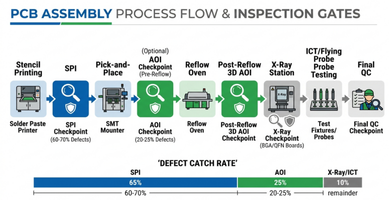
A good solder joint inspection system is more than just a tool for identifying poor joints; it's a system that allows parts of the process to improve. If an AOI machine identifies that the solder on a particular location is not sufficiently good, the engineer will investigate the cause and either replace the stencil or solve the problem with the paste before hundreds of boards are damaged. Inspection is not a gate at the end of the process, but is an active diagnostic tool.
The Real Cost of Ignoring Solder Defects
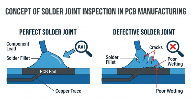
Solder defects are anything but failures waiting to occur. A cold solder joint may pass the power-on test, but upon thermal cycling, this high-resistance joint causes intermittent dropouts that are difficult to troubleshoot.
The financial math is pretty straightforward: it's only a few cents to repair a joint when it's being assembled, and hundreds of dollars when it's found after the ship has been delivered and the warranty period is over. For medical or automotive electronics, the consequences go beyond financial loss to life. That's why IPC-A-610 and IPC J-STD-001 establish specific reliability classes. Class 3 requirements are necessary because of the acceptance of no failures in a field application where safety is involved.
Types of Solder Joint Defects You Need to Know
The initial phase in effective solder joint inspection is to comprehend the defect landscape. The following are the most common production floor problems:
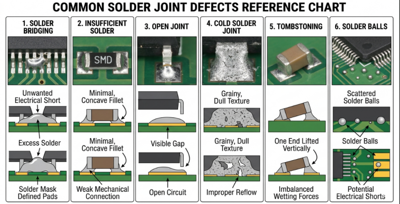
- Solder bridging: Soldered connections between neighboring pads (occurs on fine pitch QFP, passives). Sets up a short circuit for a quick or delayed malfunction.
- No solder: Joint is not made with soldering and is subjected to thermal cycling.
- Open joints: No electrical link between the component terminal and pad due to poor wetting or surface contamination.
- Cold joints: Solder that has not melted or wetted the surfaces, resulting in a grainy appearance and weak joint.
- Tombstoning: One end of the chip piece gets lifted from the pad during the reflow process, resulting in an open circuit.
- Head-in-pillow (BGA): Deposit solder ball and solder paste together, but the solder ball does not completely overlap the solder paste, so that the contact appears to be a true ball joint connection, while the soldering strength is not significant.
- Solder balls: Small spheres that come loose from joints and can cause a short.
The following table provides a summary of the defect types, their causes, and the best method of detection.
| Defect Type | Common Causes | Detection Method | Risk Level |
|---|---|---|---|
| Solder bridging | Excess paste, tight pitch | AOI, visual | High -- short circuit |
| Insufficient solder | Stencil wear, low paste volume | 3D AOI | Medium -- weak bond |
| Open joint | Contamination, poor wetting | AOI, ICT | High -- no connection |
| Cold joint | Low reflow temperature | Visual, AOI | Medium -- intermittent |
| Tombstoning | Thermal imbalance, pad asymmetry | AOI | High -- open circuit |
| Head-in-pillow | BGA warpage, oxidation | X-ray only | High -- latent failure |
| Solder balls | Outgassing, paste splatter | AOI, visual | Low to medium |
Hidden Defects: The Challenge of BGAs, QFNs, and HDI Boards
In this presentation, we will discuss the problems associated with BGA, QFN, and HDI boards and how to address them. Not all soldering faults are obvious. Some of the most dangerous ones are under component packages, which are not covered by the camera or the human eye. That's where the inspection of PCB solder joints becomes a challenging task.
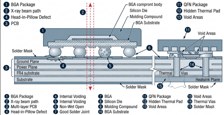
The most prominent one is Ball Grid Array (BGA) packages. There are hundreds of solder balls under the component body, and they are not visible after the component is soldered. The defects, such as head-in-pillow, internal voiding, and non-wet open, need to be inspected by X-ray.
These are similar to QFN (Quad Flat No-Lead) packages. The thermal pad on a QFN's bottom surface serves as both grounding and heat dissipation; however, it is not visible post-reflow. Thermal performance and reliability drop drastically if more than 25-50% of the pad surface is occupied by voids.
VIP (via-in-pad) HDI boards increase the complexities. A lack of solder in unfilled vias during reflow can allow solder to be drawn away from surface solder connections, creating conditions where there is not enough solder to make a good solder joint that is hard to detect without cross-sectioning.
How 3D AOI Inspection Works
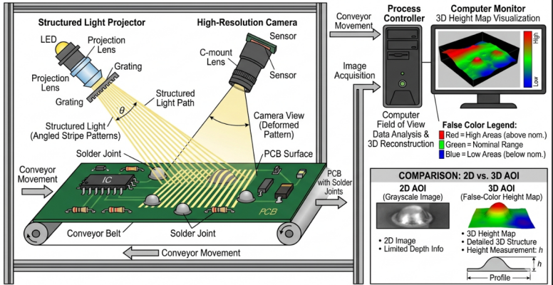
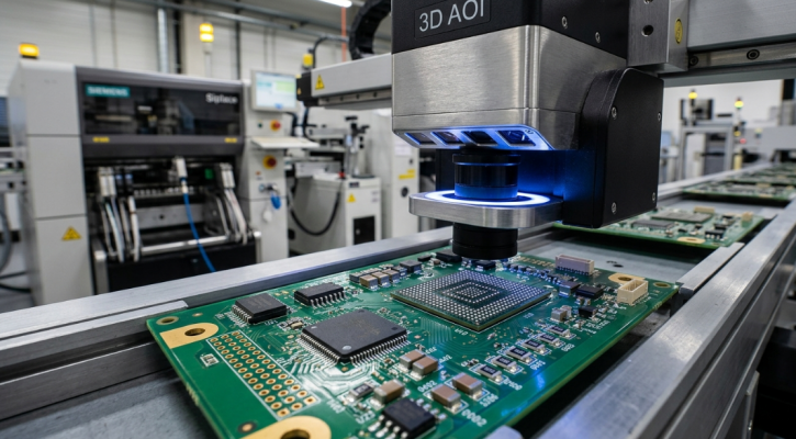
Automated Optical Inspection (AOI) has been a staple for PCB assembly for many years, but the 3D AOI systems are no ordinary 2D systems. 2D AOI is able to capture flat images and compare them to a set of reference images, useful for missing components but not for solder volume and fillet shape, resulting in high false call rates. 3D AOI overcomes this by projecting structured light, using laser triangulation or phase-shift profilometry to obtain true height information and measure solder volume, fillet shape, and wetting angles directly. Here is a side-by-side comparison of the two approaches:
| Capability | 2D AOI | 3D AOI |
|---|---|---|
| Measurement basis | Flat image analysis | Height and volumetric data |
| Solder volume accuracy | Estimated indirectly | Measured directly |
| Fillet shape evaluation | Limited to silhouette | Full 3D surface profile |
| False call rate | 5-10% typical | Below 1-2% |
| Tombstone detection | Good | Excellent |
| Coplanarity measurement | Not available | Available |
| Throughput | Fast | Comparable to 2D |
Modern 3D AOI applications can inspect at speeds of more than 60 cm per second and can export data in real-time into SPC (Statistical Process Control), enabling the engineer to see trends and intervene before defects are created.
X-Ray Inspection: Seeing What Optics Cannot
When surface inspection is exhausted, X-ray inspection (AXI) can be called on to search the interior of the component body to see the inner structure of the joint. Here are the scenarios where X-ray inspection PCB analysis is indispensable:
- Solder balls under the package (BGA & micro-BGA packages)
- The QFN and DFN packages are examples of those having hidden thermal pads.
- Double-sided assemblies with unknown optical access to barrel fill.
- The use of Package-on-Package (PoP) stacking in smartphones and IoT modules
- Any application that calls for quantitative voiding analysis for reliability compliance purposes
There are 2 modes. 2D X-ray provides a transmission image, which is fast to determine the presence of BGA balls and to identify bridges. 3D CT (Computed Tomography) produces cross-sectional slices of material at any plane to measure and detect voids with accuracy. The individual void area should not be more than 25% of the cross-section of the ball.
IPC Standards That Govern Solder Joint Acceptability
Standards are essential to any discussion of inspecting solder joints and are the criterion for determining a good solder joint. IPC-A-610 is the main reference, and there are three classes of acceptability:
- Class 1: General Electronic Products: Consumer products in which the essential function occurs at the point of sale.
- Class 2: Dedicated Service Electronic Products: Industrial/commercial equipment with a longer life span but with an acceptable amount of downtime.
- Class 3: High-Performance Electronic Products: Aerospace, military, and medical devices where downtime is unacceptable.
The requirements for the dimensions, wetting angles, and void percentages within each class get increasingly higher. The initial decision that is made when setting up any solder joint inspection system is what IPC class to choose, as it affects every pass/fail threshold.
Building a Layered Inspection Strategy
One of the common mistakes made in the PCB assembly is considering the inspection as just one point at the end of the line. The best ones are the ones that spread out the inspection throughout several stages:
- Solder Paste Inspection (SPI): After the stencil printing process. Measures the height, volume, and position of each measure. Most downstream solder defects will be caused by defects that were pasted here.
- Pre-reflow AOI (Optional): Point in time after pick and place but before reflow. Verifies the presence, orientation, and placement of components.
- Post-reflow 3D AOI: First solder joint inspection step. Checks all the joints that are visible for: bridging, inadequate soldering, tombstoning, and cold joints.
- X-ray inspection: If the board has a BGA, QFN, or hidden-joint package. May be 100% or sampling-based, depending on product type.
- ICT or Flying Probe: Electrical verification for ensuring that joints are not only visually acceptable, but electrically functional as well.
- Final Quality Control (FQC): Magnification human visual inspection prior to packaging.
The layered approach is a fundamental principle: prevention is more economical than detection, and detection is much more economical than field failure.
How JLCPCB Implements Professional Solder Joint Inspection
JLCPCB's SMT lines are designed with an inspection workflow of multiple stages, which is aligned with the best practices mentioned above. Every board is assembled and then subjected to SPI, 3D AOI, and X-ray inspection (BGA/QFN designs) – 100% board-level inspection from 5 prototypes to 5,000 production boards.
SPC data from AOI and SPI directly feed into process optimization, identifying any trends before they become defect sources. Reflow profiles are optimized for each board configuration for uniform joint formation. The on-site assembly process begins at $6, and it can be finished within 1-2 days, which makes it easy for JLCPCB to provide professional-grade inspection at any level. With EasyEDA integration, you can get from design to inspected boards with little hassle, and the instant quoting feature saves you a lot of time.
FAQ about Solder Joint Inspection
Q: What is solder joint inspection, and why is it important?
Solder joint inspection is the evaluation of solder connections on an assembled PCB to verify each joint is electrically sound, mechanically reliable, and free from defects. It matters because even one defective joint can cause field failures, and catching defects during production is far cheaper than warranty returns.
Q: What is the difference between 2D AOI and 3D AOI for inspecting solder joints?
2D AOI captures flat images and uses pattern matching, while 3D AOI adds height measurement through structured light or laser triangulation. 3D AOI directly measures solder volume, fillet geometry, and coplanarity, resulting in fewer false calls (below 1-2% versus 5-10% for 2D) and more reliable detection.
Q: When should X-ray inspection be used instead of optical methods?
X-ray inspection is essential when a board contains components with hidden solder joints BGAs, QFNs, DFNs, or through-hole joints on double-sided assemblies. It is also required for quantitative voiding analysis in reliability-critical applications.
Q:Which IPC standards define solder joint acceptability criteria?
IPC-A-610 (Acceptability of Electronic Assemblies) is the primary standard, defining three classes of acceptability with progressively stricter requirements for joint quality.
Conclusion
Inspection of solder joints is a basic necessity in any PCB assembly that is required to function properly. SPI detects paste issues at the source, 3D AOI allows for volumetric measurement of each visible joint, and X-ray imaging provides visibility of defects below BGA and QFN that no optical method can access.
With packages getting smaller and board densities increasing, engineers who know how to apply these levels of inspection and operate in conjunction with manufacturers who can deliver will continue to send out more reliable goods. For the next design that requires such a high standard of quality, the high-level inspection facilities and transparent pricing offered by JLCPCB serve as a solid foundation.</p
Keep Learning
Why PCB Inspection Microscopes Matter in Electronics Manufacturing
Key Takeaways Precise Faults: ICT tests individual components to report exact pin-level failures. Layout-Driven: Coverage relies on test pad size, pitch, and component clearance. Speed vs. Tooling: Bed-of-nails tests in seconds; flying probe requires no custom fixture. Guarded Isolation: Isolates components from parallel paths to catch early defects. Layered QA: Pairs with AOI and AXI for full quality coverage. A PCB inspection microscope earns its place on a production line because the costliest defe......
PCB Delamination Explained: Causes, Detection, and Prevention
Key Takeaways Causes: Moisture turns into steam during 260C reflow, causing layer separation under thermal expansion. Materials: High-temp lead-free builds require mid/high-Tg laminates instead of standard FR4. Detection: Surface blisters are visual, while internal voids need acoustic testing or microsectioning. Prevention: Protect bond strength using balanced copper, proper press profiles, and dry packaging. Fixes: Epoxy repair only works on minor surface defects; internal splits require board replac......
Key Benefits of In-Circuit Test in High-Yield PCB Manufacturing
Key Takeaways Precise Faults: ICT tests individual components to report exact pin-level failures without booting firmware. Layout-Driven: Coverage depends on layout rules like test pad size (0.9-1.0 mm), pitch, and clearances. Fixtures vs. Probes: Bed-of-nails runs in seconds for high volume; flying probes require zero tooling for prototypes. Guarded Accuracy: Guarding isolates components from parallel paths to detect bad values early and lower rework costs. Layered QA: Combining ICT with AOI and AXI ......
Why PCB Test Coupons Are Critical for Reliable Board Manufacturing
Key Takeaways Sacrificial Testing: Coupons allow destructive tests without harming active boards. True Process Mirror: They match the exact stackup and density to reflect panel quality. Clean Measurements: Straight lines enable precise TDR impedance and via inspection. Quality Shield: Coupon failures isolate flawed panels before shipping. A PCB test coupon is the one piece of your order that is intentionally destroyed. It rides in the panel border beside your boards, so it sees every drill, plating, a......
How to Master PCB Impedance Testing for High-Speed Designs
Key Takeaways Verification via TDR: Impedance testing uses Time-Domain Reflectometry (TDR) on test coupons to verify high-speed traces. Real-World Factors: Actual impedance is shifted by manufacturing variables, including trace undercut, solder mask, and pressed dielectric thickness. Design-to-Fab Loop: Use the manufacturer's exact stackup Dk values for layout and TDR reports to refine revisions within $\pm 10\%$ tolerance. An impedance test can be the difference between a USB 3.0 link that works reli......
Guardians of Quality: A Complete Walkthrough of PCB Inspection Standards
Key Takeaways Layered Defense: Combining AOI, AXI, ICT, and FCT covers all inspection blind spots. Paste Printing: Solder paste causes up to 60% of defects, making early checks vital. IPC Standards: IPC Class 3 tightens BGA void limits from 25% to 10%, raising costs. Thermal Balance: Equal layout heating balances reflow pull to prevent tombstoning. Design Control: Clear test pads and visible polarity marks ensure reliable automated checks. PCB inspection is not one check performed at the end of produc......