Optimizing Plating Thickness for Superior PCB Durability and Performance
13 min
- Understanding Plating Thickness in PCB Manufacturing
- How Plating Thickness Affects PCB Performance
- Industry Standards and Recommended Plating Thickness
- Key Factors Influencing Plating Thickness Quality
- Design and Manufacturing Best Practices
- JLCPCB's Expertise in Precision Plating Thickness Control
- FAQ about Plating Thickness
- Conclusion
Key Takeaways
- Plating thickness directly determines PCB durability, via reliability, and current-carrying capacity.
- Minimum hole wall copper: 20 µm (Class 2) / 25 µm (Class 3) per IPC-6012.
- Thicker copper (2 oz) significantly improves thermal performance and mechanical strength.
- Uniform plating requires good aspect ratio and process control to prevent cracking.
- Proper surface finish selection and reliable manufacturing are essential for long-term performance.
Why do two boards that are the same act differently in the field? One lasts for thousands of thermal cycles; the other develops cracked vias over the next couple of months. So it's mostly a matter of plating thickness, the thin layers of metal that conduct your current, prevent your pads from oxidizing, and bind your vias together. One of those specifications is the thickness of the plating that determines whether your board is successful.
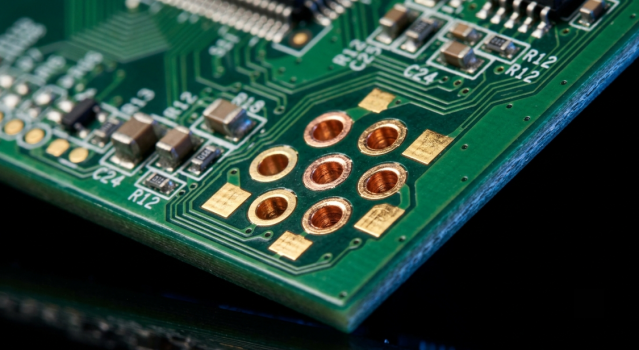
It determines the amount of current your copper can carry, how well solder joints form, and how long connectors last through multiple mating cycles. However, it is seldom focused on during design reviews. In this guide, we'll delve into the meaning of plating thickness, its impact on PCB performance, and the recommended standards. We will also be going over the factors that influence quality, a few tips for practical DFM, and how JLCPCB maintains the thickness control across all finishes and volumes.
Understanding Plating Thickness in PCB Manufacturing
It is important to understand what plating thickness is and where you can find it on a finished board before you can optimize it.
What Plating Thickness Means and Where It Is Applied
In the simplest terms, plating thickness is the amount of the metal that's applied to a surface during the manufacturing process. It is typically expressed in micrometers (µm) with older documents sometimes using microinches (µin), where 1 µm is approximately 39 µin.
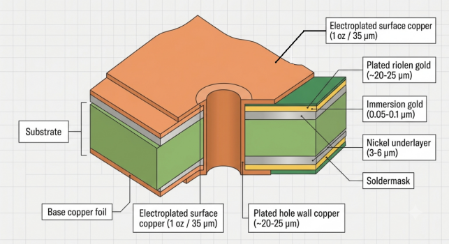
Plating can be seen in various locations on a PCB, and there are different desired thicknesses:
- The copper within drilled vias and through-holes that connect layers electrically is the hole wall of copper.
- Surface Copper: The electroplated copper, which is added to the outer layers as a trace and pad thickness.
- Surface finish: The protective coating (gold, tin, silver, or solder) that is added to bare copper to maintain solderability.
- Edge connector plating: Thicker, harder gold on gold fingers that can take repeated insertion.
There's a purpose to each layer. If you get the thickness wrong on any of them, you'll be exposed to defect types ranging from weak solder joints to open circuits in a via.
Copper Plating vs Surface Finish Plating
It helps distinguish between the two large groups, since they employ different chemistries and have different goals. Copper Plating adds the conductive backbone to the board, and surface finish plating protects the copper and allows for assembly. The copper plating is an electrolytic process, which thickens the copper in the holes and in the outer traces. This is where the current carrying capacity and the via reliability are derived from.
A typical outer layer is thin foil and is then plated to a finished weight of 1 oz ( ~35 µm) or 2 oz ( ~70 µm). In contrast to surface finish plating, which is a thin protection layer that is measured in parts of a micrometer to a few micrometers. Surface Finishes and Plating include such coatings as ENIG, HASL, OSP, immersion silver, and immersion tin, which prevent the copper from becoming corrosion-prone or losing its ability to be soldered before the assemblies are made.
How Plating Thickness Affects PCB Performance
Plating thickness is no frivolity; it's a performance factor that directly affects the electrical, thermal, and mechanical performance of your board.
Impact on Current Carrying Capacity, Reliability, and Signal Integrity
The thicker the copper, the more current it can carry, and the less the temperature will rise. The IPC-2221 charts indicate that a 1oz trace and a 2oz trace, of similar trace width, have similar, but not identical, current-carrying capacities before heating. Plating is added onto that copper, and the thickness is consistent, which translates to predictable current ratings. Reliability is in your vias. Copper borehole withstands z-axis expansion with each heating and cooling of the board. If it is too thin, then micro-cracks form, and if it is too uneven, the stress concentrates at the weak point.
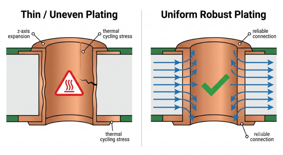
This is why IPC-6012 provides a minimum requirement for the average thickness of the hole wall in copper of approximately 20 µm for Class 2 and 25 µm for Class 3 boards. The thickness of the plating is directly felt on the signal integrity. A few micrometers of change in the thickness of copper can change the trace impedance by a few ohms, which can result in reflections if the line is a controlled-impedance line, and if the frequency is greater than 100 MHz. The skin effect begins to become important, and that means plating uniformity at GHz frequencies because the current is confined to a shallow surface layer.
Relationship with Thermal Management and Mechanical Strength
The thickness of the plating has an impact on the board's ability to remove heat from its hotter elements, as copper is a good heat spreader material. Heavier plated copper and well-plated thermal vias reduce the thermal resistance, which helps to keep the junction temperatures under control under load.
From a mechanical point of view, a plated barrel inside a via is similar to a rivet that holds the layers together. A sturdy, even barrel withstands flexing and thermal cycling shears. Thin or nodular plating is a failure site, particularly in thick boards where the aspect ratio (hole thickness to hole diameter) is high.
Industry Standards and Recommended Plating Thickness
Standards are provided to ensure that designers and fabricators are using the same language. The reference documents for plating are IPC-6012 (rigid boards) and IPC-4552/4556 (finishes).
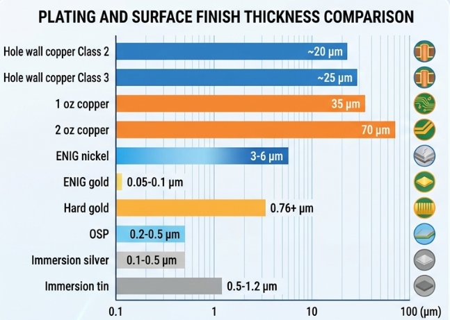
Typical Values for Different Applications and Surface Finishes
The following table shows the most common classes and surface finishes of copper plating, the typical thickness range, and the applications where they are best suited. These are typical industry values; please always check the values with your Fabricator's data sheet.
| Layer / Finish | Typical Thickness | Notes / Typical Use |
|---|---|---|
| Hole wall copper (IPC-6012 Class 2) | ~20 µm average | General commercial and consumer boards |
| Hole wall copper (IPC-6012 Class 3) | ~25 µm average | High-reliability: medical, aerospace, automotive |
| Outer copper — 1 oz | ~35 µm finished | Standard signal and low-current designs |
| Outer copper — 2 oz | ~70 µm finished | Power, high-current, better heat spreading |
| HASL / Lead-free HASL | ~1–25 µm (uneven) | Cost-effective, robust, and good solderability |
| ENIG (nickel) | 3–6 µm | Flat pads for fine-pitch, BGA, wire bonding |
| ENIG (gold) | 0.05–0.1 µm | Corrosion barrier over nickel |
| Hard gold (edge connectors) | 0.76 µm and up | Gold fingers, high-insertion contacts |
| OSP | ~0.2–0.5 µm | Flat, low-cost, single reflow assembly |
| Immersion silver | ~0.1–0.3 µm | Flat, good for RF, decent shelf life |
| Immersion tin | ~0.8–1.2 µm | Flat, fine-pitch friendly, press-fit |
Minimum Requirements for High-Reliability and High-Current Boards
When it comes to boards that can't fail, the standards are higher. Typically, high-reliability designs use IPC-6012 Class 3, which requires a minimum average hole wall thickness of 25 µm and reduces defect limits. The higher the current, the thicker the copper used in the board. Common practice includes:
- Designing for 2 oz or greater outer and inner copper to minimize resistive heating.
- Multiple and well-plated thermal vias to transfer heat under power devices.
- Seeking Class 3 hole wall plating for thermal cycling.
- Increase the width of the traces as per IPC-2221 charts to accommodate the thicker copper and increased ampere flow.
Key Factors Influencing Plating Thickness Quality
It's easy to score a certain number on a piece of paper. The ability to achieve that thickness consistently on a full panel, after each and every batch, is the true testament of the skill of manufacturing.
Process Parameters, Chemistry Control, and Equipment Precision
The physics and chemistry that govern electroplating are within a very narrow range. The uniformity of copper deposition is influenced by current density, bath temperature, agitation, and additive concentration.
There are a number of parameters that need continuous attention:
- The distribution of current (current density): Edges become thicker than the center due to uneven current.
- Bath chemistry: Copper, acid, and organic additive levels will need to be titrated on a regular basis.
- Pulse or periodic-reverse plating: Aids in the throwing of copper into high aspect ratio holes.
- Anode-to-cathode geometry: Deposition uniformity is maintained in the desired panel by proper fixturing.
- Filtration and temperature control: Avoid the formation of nodules and rough, brittle deposits.
These variables are maintained stable by precision equipment with automated dosing and inline monitoring.
Common Defects from Incorrect Plating Thickness
Thickness can be wrong - the defects are often not apparent until test or field failure. Early identification helps to avoid scrap and recover.
- Thin hole wall copper: Leads to via cracking and open circuits during thermal cycling.
- Over-plating: Reduces spacing, solder mask registration problems, and flux entrapment.
- Nodules and roughness: Due to poor chemistry, which affects impedance and appearance.
- Gaps in plating that form poor connections: Voids in the barrel.
- Gold is too thin on connectors: Nickel wears through, giving intermittent contact.
Design and Manufacturing Best Practices
Good plating begins with the schematic and layout, well before the board gets to a plating tank. With a couple of choices you can make, you can make the job of the manufacturer easier, and your yield will be higher.
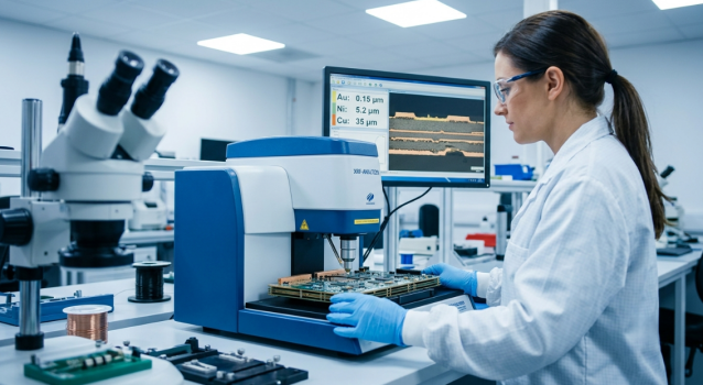
DFM Guidelines for Plating Thickness Optimization
Design for Manufacturing (DFM) is all about giving the fab process a fighting chance of achieving your targets. With plating, design is as important as it is in reliability.
Here are some DFM points to consider:
- Control aspect ratio: Make hole depth/diam reasonable (usually 8:1 to 10:1) to ensure reaching the barrel center.
- Even copper distribution: Even copper across the panel promotes uniformity and minimizes bowing.
- Match trace width to copper weight: The heavier the copper, the wider the spacing because of sidewall etching.
- Choose appropriate finish: Flat finish (ENIG, OSP) if using fine pitch BGA, hard gold if using edge connectors, etc.
Quality Control, Measurement, and Verification Methods
We cannot control that which we cannot measure. There are multiple complementary processes that fabricators use to validate plating thickness as required.
- X-Ray Fluorescence (XRF): Quick and non-destructive surface finish and copper measurement, with an accuracy of approximately ± 0.1 µm.
- Microsection (cross-section) analysis: Destructive but definitive – gold standard for hole wall copper.
- Eddy current testing: Fast, non-destructive tests, but not as accurate below 1 µm.
- Coupon testing: Special test coupons on the panel are subdivided to represent the batch.
The inline monitoring with periodic micro sections provides both real-time control and traceable evidence that the board is within spec.
JLCPCB's Expertise in Precision Plating Thickness Control
Knowing the theory is one thing; applying it is another. This is where a manufacturing partner with experience comes into play, converting plating specifications into consistent and repeatable results.
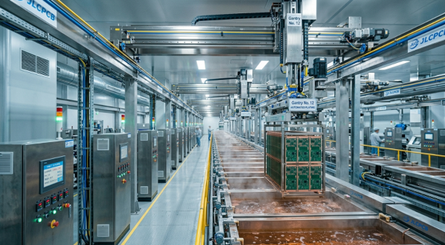
Advanced Plating Lines with Strict Thickness Monitoring
JLCPCB operates modern and automatic plating lines and controls the chemistry and conducts online monitoring. Copper plating is controlled to ensure predictable hole wall copper in the ~20-25µm range, which meets the IPC-6012 Class 2 standards for normal construction, and is suitable for more stringent requirements when required. The finished outer copper comes in 1 oz and 2 oz sizes, providing a clear choice between standard signal board and higher current and/or better heat-spreading designs. Uniform current density control over the panel ensures uniform thickness from the edge to the center.
Comprehensive DFM Review Focused on Plating Requirements
All orders undergo an automated and engineering DFM review before production. This check identifies high aspect-ratio holes, unbalanced copper, and finish options that may affect the quality of the plating. This is an up-front review, which will identify issues that would otherwise manifest as field failures. It can help you match the surface finish to your assembly process, eliminating surprises in solderability.
Consistent High-Quality Results Across All Surface Finishes and Production Volumes
JLCPCB provides a complete range of surface finishes: HASL, lead-free HASL, ENIG, OSP, and immersion silver/tin on suitable products, with consistent thickness targets. For flat, solderable pads, for instance, ENIG has the same nickel (3–6 µm) and gold (0.05 - 0.1 µm) structure as is known. The same controlled processes are followed for a small quantity of prototypes as well as thousands of production boards. To implement these plating concepts, JLCPCB's instant quoting feature and the feedback it provides for DFM requirements ensure it is easy to secure the correct copper weight and finish for your design.
FAQ about Plating Thickness
Q: What is the plating thickness on a PCB?
Plating thickness is the depth of metal deposited onto a surface during manufacturing, measured in micrometers. It applies to whole wall copper, outer surface copper, and protective surface finishes like gold or tin.
Q: What is the minimum copper plating thickness for reliable vias?
IPC-6012 sets a minimum average hole wall copper of about 20 µm for Class 2 boards and 25 µm for Class 3, high-reliability boards. Staying above these values helps vias survive thermal cycling without cracking.
Q: How thick is the gold layer in ENIG?
In ENIG, the gold layer is very thin, typically 0.05–0.1 µm, sitting over a nickel layer of about 3–6 µm. The gold only acts as a corrosion barrier, while the nickel provides the solderable, wear-resistant surface.
Q:Does thicker copper plating improve signal integrity?
Not always — beyond a point, thickness gives diminishing returns because high-frequency current flows in a thin skin layer. What matters most for signal integrity is uniform, consistent plating that keeps controlled impedance on target.
Q: How is PCB plating thickness measured?
Common methods include X-Ray Fluorescence (XRF) for fast non-destructive checks and microsection analysis for definitive hole wall copper verification. Eddy current testing offers quick surface checks but is less reliable for very thin layers.
Conclusion
The thickness of the plating can be in the micrometer range, but the effect on your board is far from insignificant. Whether it's the copper barrel that holds your vias together or the thin gold that keeps pads solderable, each layer helps to ensure durability, current capacity, and longevity. The difference between boards that merely work and boards that last is that plating is not an afterthought; it is viewed as a first-class design parameter.
As electronics evolve toward higher currents, smaller pitches, and harsher environments, precise plating control will become even more critical. Combine good knowledge of IPC standards and a manufacturer that takes thickness seriously, and you have a foundation for your design. As soon as you're prepared to build, JLCPCB's controlled plating lines, clear weights of copper, and full line of surface finishes make it easy to translate these principles to hardware you can trust.
Keep Learning
Choosing the Right Surface Finish for Your PCB: An Overview of HASL, ENIG, OSP, Immersion Tin and Immersion Silver
Key Takeaways Lead-Free HASL: Best low-cost, RoHS-compliant finish for general PCB builds. ENIG: Superior flatness and 12+ month shelf life for fine-pitch BGAs. OSP: Ultra-flat, lowest-cost option for high-volume SMT (3–6 month shelf life). Immersion Silver: Ideal for high-frequency RF by eliminating nickel signal loss. Immersion Tin: Best for press-fit connectors and fine-pitch assembly. Printed Circuit Boards (PCBs) are essential components in the manufacturing of electronic devices ranging from sma......
Conformal Coating in PCB Technology: Benefits, Challenges, and Future Developments
If you're searching for conformal coating, you're likely looking for a reliable way to protect your PCB from moisture, dust, chemicals, or harsh environments. Choosing the right coating directly affects product reliability, performance, and lifespan. In this guide, you'll learn what conformal coating is, the main types available, and how to select the best option for your application. We'll also cover key benefits, application methods (manual, automated, and selective), as well as inspection, rework, ......
PCB Gold Fingers: Why They Matter and How to Design Them
Key Takeaways PCB gold fingers provide reliable electrical and mechanical contact for PCBs that connect to external connectors or card slots. ENIG is suitable for general contact applications, while electroplated hard gold offers higher wear resistance for repeated insertion and removal. Gold fingers should remain fully exposed, with solder mask and silkscreen kept away from the contact area. Proper chamfering and gold finger orientation are essential to ensure smooth insertion and prevent damage duri......
Comparing HASL and ENIG Surface Finishes for PCBs
Selecting the right surface finish for a printed circuit board (PCB) is crucial to ensuring its performance, reliability, and longevity. Two of the most commonly used finishes are Hot Air Solder Leveling (HASL) and Electroless Nickel Immersion Gold (ENIG). Each of these surface finishes offers distinct advantages and disadvantages, making them suitable for different applications. In this article, we will compare HASL and ENIG to help you determine which finish is best suited for your PCB project. What......
Avoid PCB Assembly Failures: Mastering Solder Mask Expansion Rules and Best Practices
Solder mask protects copper traces and pads from oxidation, bridges, and contamination during assembly. Incorrect solder mask expansion—the clearance around features where mask is pulled back—leads to defects like shorts or exposed copper. Engineers must set expansion values precisely to ensure reliable soldering and long-term performance. Introduction: Why Solder Mask Expansion is Critical for PCB Reliability Understanding Solder Mask and Expansion Basics Solder mask is a polymer layer applied over t......
The Ultimate Guide to OSP Surface Finish in PCB Manufacturing: Advantages, Process, and Selection
Key Takeaways OSP (Organic Solderability Preservative) is a water-based, cost-effective PCB surface finish that deposits a 0.2-0.5μm organic film directly onto copper pads. Unlike metallic finishes such as ENIG or HASL, OSP provides superior surface flatness for fine-pitch SMT components at no extra process charge, making it ideal for high-density consumer electronics. However, OSP requires controlled handling and a limited assembly window (24-48 hours after opening vacuum packaging). It is best suite......