
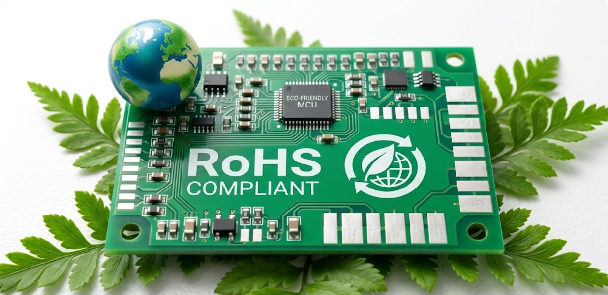
How Sustainable Materials and Expert Manufacturing Ensure RoHS Compliant PCBs
12 min
- Why RoHS Matters for Environmental Safety and Market Access
- Impact of RoHS on PCB Materials and Components
- Building RoHS Compliance into PCB Design and Production
- Achieving Superior RoHS PCBs Through Advanced Manufacturing
- JLCPCB’s Commitment to RoHS Excellence and Sustainability
- Frequently Asked Questions (FAQ)
Have you ever experienced that a finished shipment of products was detained at the EU customs due to a single component on the board not passing the RoHS screening? It is higher than most engineers think, and the financial blow is far bigger than the impounded goods. Wasted time, remodeling expenses, and a compliance audit that is capable of halting your whole product introduction, that is the actual cost of doing RoHS wrong. The point is as follows: RoHS-compliant PCBs cease to be a checkbox exercise for experienced PCB designers. The mandate has already become a discontinuous regulation to a highly integrated manufacturing fact that pervades every material selection, every process parameter, and every connection in your supply chain.
The technicalities of doing it right continue to take experienced teams by surprise. Today, we are going to explore the material science, process control, and supply chain strategies that make the difference between the truly compliant boards and those that seem to be compliant on paper. This guide includes the practical engineering details that are important, whether it is with lead-free alloy selection, reflow profiling, or even with compliance documentation.
Why RoHS Matters for Environmental Safety and Market Access
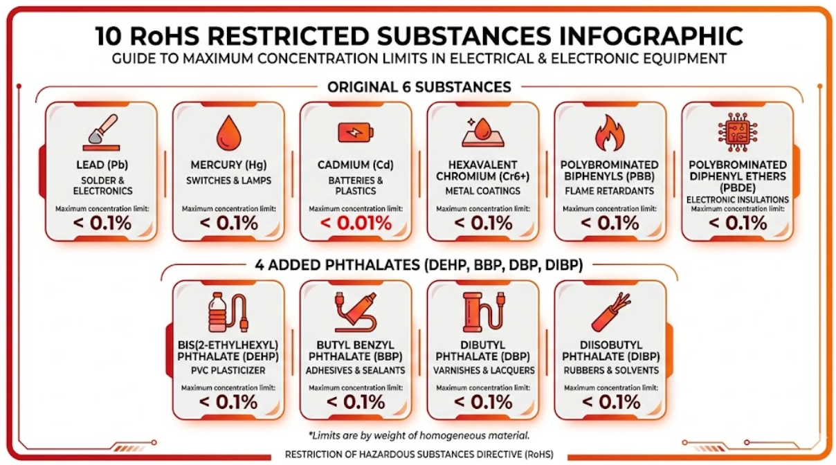
As we have observed in class, the Restriction of Hazardous Substances Directive (2011/65/EU, which was amended by 2015/863/EU as RoHS3) puts a limit on ten chemicals in electrical and electronic equipment. The six constituent substances, which are lead (Pb), mercury (Hg), cadmium (Cd), hexavalent chromium (Cr6+), polybrominated biphenyls (PBB), and polybrominated diphenyl ethers (PBDE), are originally restricted to 0.1% by weight in any homogeneous material, with the exception of cadmium being restricted to 0.01%. Four phthalates, namely DEHP, BBP, DIBP, and DBP, were then added by RoHS 3, with a limit of 0.1 per cent. Each.
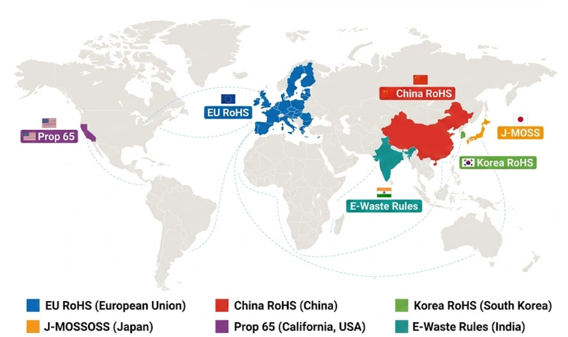
It turned out that it goes far beyond Europe. China has a local variant of RoHS, Japan has a J-MOSS, South Korea has a resource-recycling act, and the state of California has a similar limit in its Proposition 65. When we develop products to comply with RoHS, we can effectively sell them to any country with a substantial market; otherwise, we can only find a small number of exemptions in Annexes 3 and 4. Lead has actually rewritten the playbook in PCB fabrication and assembly. Replacement of the traditional Sn63/Pb37 eutectic solder with lead-free alloys not only raised reflow temperatures but also altered wetting behavior and disrupted reliability issues that the industry had struggled to balance over the decades.
Impact of RoHS on PCB Materials and Components
Lead-Free Solder Alloys: The Material Trade-Offs That Matter
The transition from Sn63/Pb37 (183C eutectic) to SAC305 (Sn96.5/Ag3.0/Cu0.5, liquidus 217-220C) is the most consequential RoHS-driven material change. But SAC305 is not the only option.
| Alloy | Composition | Liquidus (C) | Key Characteristics |
| SAC305 | Sn96.5/Ag3.0/Cu0.5 | 217-220 | Industry standard, good reliability, higher cost (silver) |
| SAC105 | Sn98.5/Ag1.0/Cu0.5 | 227 | Lower cost, slightly reduced fatigue life |
| SN100C | Sn/Cu0.7/Ni0.05/Ge | 227 | Silver-free, good wetting, popular for wave soldering |
| SnBi | Sn42/Bi58 | 138 | Low-temperature option for sensitive components |
SAC305 is essentially the one that will be used due to its ability to balance wetting, reliability, and fit into the process. SAC105 and SN100C are beginning to gain some ground when it comes to budget-sensitive, high-volume work, as the silver in those is adding a discernible additional price.
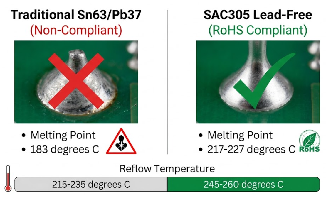
The 34 -37 °C shift in liquidus temperature introduces a great deal of variables into the equation. Components must now withstand a peak reflow temperature of 245-260°C rather than 215-235 °C, as was the case with the former leaded components. Wetness sensitivity becomes infinitely worse - any water that gets into it expands significantly faster at such temperatures, increasing the risk of popcorning in ICs with plastic cases. And since the alloys without lead dry less, the design of the pad and the choice of surface finish are more significant than ever before when we were using lead.
RoHS-Compliant Surface Finishes: Selection and Trade-Offs
Every RoHS-compliant surface finish eliminates lead, but each brings distinct engineering trade-offs. Selecting the right finish depends on your assembly process, shelf life requirements, and end-use environment.
| Surface Finish | Shelf Life | Flatness | Cost | Best For |
| Lead-Free HASL | 12+ months | Moderate | Low | General-purpose, through-hole heavy designs |
| ENIG | 12+ months | Excellent | Medium-High | Fine-pitch BGAs, wire bonding, and long storage |
| OSP | 6 months | Excellent | Low | High-volume, single-reflow assemblies |
| Immersion Silver | 6-12 months | Excellent | Medium | RF/microwave, membrane switch contacts |
| Immersion Tin | 6 months | Excellent | Medium | Press-fit connectors, backplanes |
It seems that ENIG has become the preferred choice, as far as complex assemblies are concerned, as we have learned in the lab. It is very flat to fine-pitch components, has good shelf life, and has a good nickel diffusion barrier that is typically 3. The downside? It is expensive, and you are likely to risk black pads unless the nickel deposition has been nailed down.
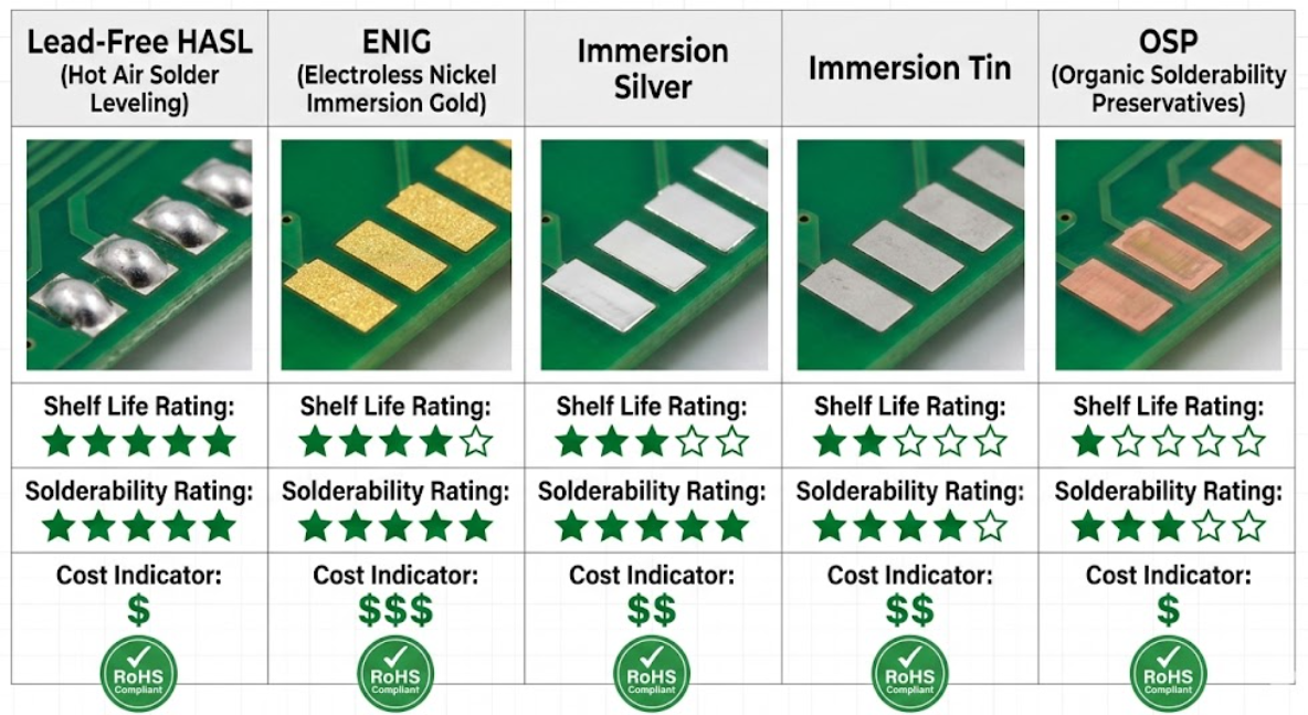
Conversely, OSP is the low-cost RoHS alternative and has rather decent flatness. The trick is that its protective coating is worn off with each thermal cycle, meaning that with reflow on both sides you may get halfway through the second reflow before the OSP on the first pass is completely removed. Fortunately, we students can count on recent PCB manufacturers such as JLCPCB, which offer all the significant RoHS-compatible finishes, and it becomes easy to select the appropriate one to use in your project.
Pro-Tip: If your design mixes fine-pitch BGAs with standard SMT and through-hole components, ENIG is almost always the safest choice. The higher material cost is offset by reduced assembly defects and better yield on fine-pitch joints.
Halogen-Free Laminates: Design Implications Engineers Should Know
Normal FR-4 tends to receive flame-retardant in tetrabromobisphenol A (TBBPA). It is not amongst the chemicals that RoHS completely prohibit, but many people are replacing it with halogen-free alternatives due to the WEEE regulations and even some pressure to go green in procurement. The specification of the IPC/JEDEC J-STD-709 states that halogen-free indicates less than 900ppm of any one of the two chlorine and bromine, and the halogen content cannot exceed 1500ppm in total.
From a design perspective, halogen-free laminates introduce measurable differences:
- Dielectric constant (Dk): Typically 0.1-0.3 higher, requiring impedance recalculation for controlled-impedance traces.
- Moisture absorption: Can be 20-40% higher, increasing delamination risk during lead-free reflow.
- Tg: Modern halogen-free laminates achieve 150-180C, on par with mid-to-high Tg FR-4.
- Z-axis CTE: May be slightly higher, relevant for thick multilayer boards with many via transitions.
Building RoHS Compliance into PCB Design and Production
Designing for Lead-Free Assembly: Practical DFM Considerations
When we discuss increased temperatures, the differences in wetting lead-free solder, we, in fact, refer to the fact that the design will have to be more deliberate. The result is that lead-free solder has a larger contact angle, randomly 30-45 degrees on SAC305 versus 10 -20 degrees on the traditional Sn63/Pb37, thus it simply does not spread out on the pad surface as easily.
With thermal pads on QFN and BGA, that diminished wetting may leave these irritating voids in case the stencil aperture structure is not optimized. A windowed or segmented aperture pattern - dividing the large thermal pad aperture into a grid of smaller ones - allows the flux gases to escape during reflow to minimize voiding. IPC-7351 pad guidelines tend to be stable, but it is high time you paid a little more attention to thermal pad design.
Component Sourcing and Supply Chain Verification
The quality of a RoHS-compliant board is as good as its weakest component and we need to press-check each component. Get material declarations of all component suppliers (typically IPC-1752) and ensure that the stock of any distributor is not some ancient leaded stuff, establish incoming inspection checks to intercept any non-compliant parts before they reach on to the production line, and create a traceable database listing the status of each component and material. It may seem like a lot of documentation, however, a single non-conformance may destroy the compliance of the entire product and lead to expensive market access problems that we do not need.
Testing Protocols for Hazardous Substance Detection
We begin with X-ray fluorescence (XRF) to get a snap shot on high-level restricted substances- XRF determines the elemental composition. To determine the definitive read, we resort to wet chemistry (ICP 3 -ES or ICP 3 -MS) to obtain precise quantitative data on those outlawed elements.
Phthalate tests are more difficult and expensive: we perform solvent extraction and then GC-MS. Due to its high cost, we normally execute it on representative samples rather than all the batches. The frequency of our test will be based on your quality system and risk assessment. Periodic checks can be used with large-volume runs and reliable suppliers. New suppliers or materials should be tested more often before they can establish a good track record
Achieving Superior RoHS PCBs Through Advanced Manufacturing
Lead-Free Reflow Process Control and Contamination Prevention
Therefore, lead-free reflow process window is relatively narrow half the size of the previous leaded solder window, and it is that one fact that makes most of the manufacturing complexity. A typical SAC305 reflow profile targets a peak of 245-250C, time above liquidus (217C) of 60-90 seconds, preheat ramp of 1.0-2.0C/second, and cooling ramp of 2.0-4.0C/second.
It is costly to miss that window on either side. Under-heating, you get cold joints and the irritating head-in-pillow flaws on BGAs. Over‑heat? Pad lifting, measling and fast IMC growth which actually causes the joints to become brittle. That is why we have multi-zone convection ovens- 8 to 10 zones that can be adjusted individually and thermocouple-profiling to keep everything in check.
In locations where both RoHS and non-RoHS production is conducted, it is equally important to avoid contamination in the mix. The lead may be deposited in any common solder pot, stencil or rework equipment. The fix is special equipment according to the level of compliance, frequent ICP tests of the solder pot blend, and maintaining physical separation of the material flows. This is automatically addressed by the all-RoHS line of JLCPCB, so you need not be afraid of confusing non-RoHS materials.
Precise Material Handling and Contamination Prevention
Cross-contamination of compliant and non-compliant materials is an important issue that should be avoided in a RoHS manufacturing environment. Solder pots, wave solder machines and reflow ovens that have been used to run leaded assemblies should be completely cleaned and tested prior to running RoHS production. Most of the facilities maintain specific tools of RoHS and non-RoHS work to avoid the risk of contamination completely.
Material handling processes are used to guarantee that the components and materials that are stored and that are RoHS compliant are kept separate and their identification and tracking is done separately as opposed to the non-compliant components and materials. Inbound inspection ensures that all material lots are the same as their compliance documentation prior to release into production.
Comprehensive Certification and Traceability Systems
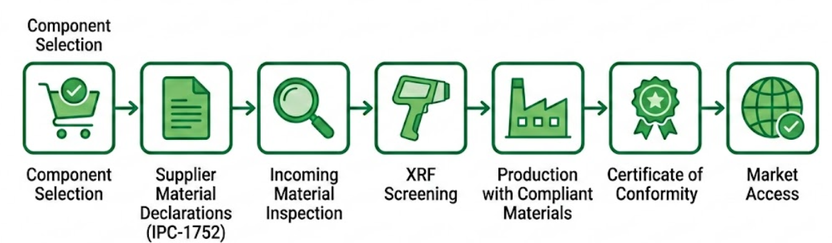
RoHS compliance documentation consist of certificates of conformity prepared by the fabricator and assembler, material test reports that prove the restricted level of substances below the threshold, component level material declaration by all suppliers and lot traceability between finished products and particular material and component batches. This documentation chain facilitates quick reaction to compliance inquiries by the customers, custom authorities or market surveillance agencies. It also helps in product recall management in case there is a compliance problem that is found post shipment.
JLCPCB’s Commitment to RoHS Excellence and Sustainability
Fully RoHS-Certified Facilities and Material Partnerships
JLCPCB therefore operates on the RoHS guidelines, boards, solder, or even the fancy finishes. The substrates, solder, surface finishes, solder mask and all the other common stuff are RoHS clean by default. They have even partnered with certified suppliers hence they do not run out of compliant parts regardless of the size of the order.
Robust Testing and Documentation for Global Compliance
Their quality system is rather sound: they maintain test materials, audit suppliers, and add a ton of paperwork to the mix in order to have you comply. Having RoHS certificates and material declarations on all the standard stuff is a great relief when you are trying to sell in controlled markets all over the world- you just grab the papers out.
Delivering Reliable, Eco-Friendly PCBs at Scale

JLCPCB issues boards with RoHS-compliant boards whether you are simply prototyping or are shooting out a million units, the quality of the boards is the same high-quality that you would get with full-scale production. And they have connections to do more than RoHS: they eliminate waste, conserve energy, and responsible handling of chemicals throughout the entire build process.

Frequently Asked Questions (FAQ)
Q. What does RoHS compliance mean for a PCB assembly?
Every homogeneous material in the assembly substrate, solder, surface finish, solder mask, component leads, and bodies. It must contain restricted substances below the maximum concentration limits.
Q. Are all JLCPCB boards RoHS compliant by default?
Yes. JLCPCB uses RoHS-compliant materials including lead-free HASL, ENIG, OSP, lead-free solder paste, and compliant substrates as standard. Non-compliant options like leaded HASL are available only on specific request for exempt applications.
Q. How do I handle legacy components only available in leaded versions?
Redesign to use a compliant alternative, apply for a RoHS exemption under Annex III or IV if your application qualifies, or source from a supplier offering a RoHS-compliant version. Most legacy components have compliant alternatives today.
Q. How often should I test for RoHS compliance?
New suppliers should be XRF-screened at qualification and periodically thereafter. Established suppliers may shift to annual verification or lot-based sampling. Phthalate testing is typically limited to representative samples during initial qualification.
Keep Learning
Solder Joint Inspection in PCB Manufacturing : A Complete Guide to Catching Defects Early
Key Takeaways Solder Joint Inspection is critical in modern PCB manufacturing to catch defects early and ensure product reliability. By combining Solder Paste Inspection (SPI), 3D AOI for visible joints, and X-ray for hidden BGA/QFN issues, manufacturers can effectively detect common defects such as bridging, cold joints, tombstoning, and head-in-pillow. Following IPC-A-610 standards with a layered inspection strategy significantly reduces field failures while improving first-pass yield. JLCPCB’s prof......
3D AOI Inspection Explained : How It Catches Defects That 2D Systems Miss
Key Takeaways 3D AOI Inspection has become essential in modern PCB assembly by using advanced height and volume measurement to detect critical solder defects that traditional 2D AOI systems routinely miss, such as lifted leads, insufficient solder, head-in-pillow, and component coplanarity issues. By delivering precise 3D data through structured light or Moire technology, it significantly reduces false calls, improves first-pass yield, and ensures long-term reliability according to IPC-A-610 standards......
How Sustainable Materials and Expert Manufacturing Ensure RoHS Compliant PCBs
Have you ever experienced that a finished shipment of products was detained at the EU customs due to a single component on the board not passing the RoHS screening? It is higher than most engineers think, and the financial blow is far bigger than the impounded goods. Wasted time, remodeling expenses, and a compliance audit that is capable of halting your whole product introduction, that is the actual cost of doing RoHS wrong. The point is as follows: RoHS-compliant PCBs cease to be a checkbox exercise......
Preventing PCB Warping: Best Practices for Design and Manufacturing
In the design and manufacturing process of electronic equipment, PCB (Printed Circuit Board) warpage is a common but troublesome problem. PCB warping not only affects the performance and reliability of the device but can also cause connectivity issues and other serious consequences. Therefore, it is crucial to understand how to prevent and resolve PCB warping. This article will explore some best practices in design and manufacturing to help you effectively prevent PCB warpage problems from occurring. ......
PCB Cleanliness in Professional Manufacturing : Preventing Contamination and Ensuring Long-Term Reliability
In the construction of PCBs, the boards are contaminated with all sorts of dirt at almost every stage. In the soldering process, the flux (either rosin-based or more recent organic forms) may cause residues or ionic salts to remain on the pads and traces and be sticky. Next there is etching, plating and micro-etching; the chemical processes will put metal ions on the copper unless the rinsing is complete. Tiny particles of metal shavings, fiberglass dust, and laminate fragments are also thrown out in ......
PCB Basics 5: PCB Testing and Quality Assurance
Welcome to the realm of PCB testing and quality assurance! Quality control is always a crucial part of different industries. Great quality control not only could generate more energy for customers’ electronic projects, but it could also embark on certification and guarantee to the electronic industry. Let’s learn the importance of testing and quality assurance in PCB manufacturing. The Significance of Testing and Quality Assurance in PCB Manufacturing: Testing and quality assurance are extremely impor......