Why PCB Inspection Microscopes Matter in Electronics Manufacturing
14 min
- Essential Roles of Inspection Microscopes in Quality Control
- Choosing the Right Microscope for Electronic Applications
- Advanced PCB Inspection Equipment and Factory Workflows
- Professional Manufacturing Practices for High-Yield PCBs
- FAQs about PCB Inspection Microscope
- Conclusion
Key Takeaways
- Precise Faults: ICT tests individual components to report exact pin-level failures.
- Layout-Driven: Coverage relies on test pad size, pitch, and component clearance.
- Speed vs. Tooling: Bed-of-nails tests in seconds; flying probe requires no custom fixture.
- Guarded Isolation: Isolates components from parallel paths to catch early defects.
- Layered QA: Pairs with AOI and AXI for full quality coverage.
A PCB inspection microscope earns its place on a production line because the costliest defects are often ones a camera has already passed. An AOI machine judges each joint from a fixed viewpoint. So a fillet of the right size that never bonded to the pad can look almost identical to a good one. The two joints differ only at the edge of the solder, because good solder spreads across clean copper and thins to a feather edge, like water on clean glass.

Figure 1: A populated PCB under a digital microscope
Solder that never touched the pad will form a circular arc, like water on a waxed car. Therefore, magnification and a tiltable view remain the determining factors for borderline joints. This guide explains what a microscope can see outside of the AOI, how to select a microscope, which specifications and lighting are best suited for which jobs, and where optical checks fit into a factory.
Essential Roles of Inspection Microscopes in Quality Control
There are three quality-control functions that a microscope can accomplish that no other instrument can do alone. It carries out firms' quality-control operations, determines whether a camera threshold is reached, and therefore predicts whether a joint that's not yet will withstand years of thermal cycling.
Detecting Microscopic Defects Beyond AOI Limits
Automated optical inspection compares each joint with a stored reference, so the result depends on the thresholds applied. The false calls increase when they are set to a tight, harmful variation in fillet shine. Let them go free, and true faults fly away. This is why each line of AOI must have a station to review it, and viewing is done through a microscope.
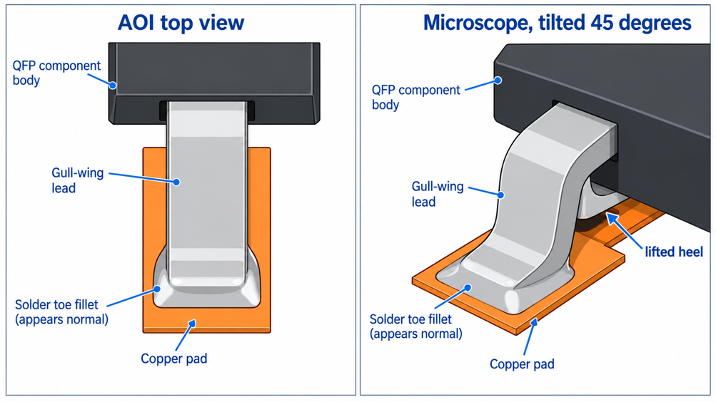
Figure 2: The same gull-wing joint seen from directly above and from a tilted microscope angle
- Viewing angle is the second limit: A 2D AOI camera looks straight down, and 3D systems add only a few fixed angles, so the part body hides some of each joint. A lifted gull-wing lead can still show a normal toe fillet from above.
- Some defects have almost no optical contrast: A flex crack in an MLCC, caused by board bending after reflow, can be fine enough to escape even a high-power microscope, so suspect parts are confirmed electrically or by cross-section.
Common Solder and Trace Defects Identified Under Magnification
There are two families of magnified rejections. There are two solder defects: one occurring during reflow or hand soldering, and the other during etching of the bare board to produce traces. Each defect type occurs at a different checkpoint. There are five recurring themes:
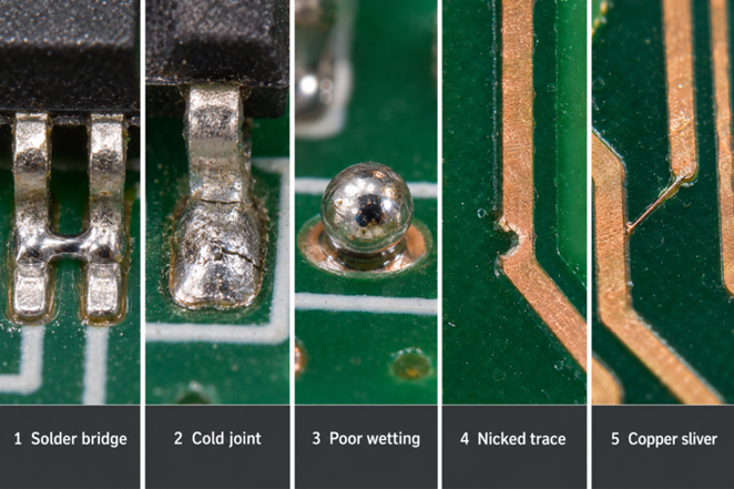
Figure 3: Five common defects seen under magnification
- Solder bridges: When a film or whisker of solder connects two adjacent pads.
- Cold joints: a grayish, porous joint, rather than a smooth fillet, which never got completely wet.
- Poor wetting: Solder that beads up with a high edge rather than spreading.
- Conductor nicks/pinholes: chewed through the edge of a trace or holes in the copper.
- Copper slivers: Unsliced copper slivers between individual traces.
The thickness of the film is most critical on fine-pitch parts, as there are still current-carrying thicknesses that are too thin to be measured by AOI. Cold joints occur when the joint does not reach a sufficiently high temperature to fully wet, leaving a weak bond that fails to withstand vibration. The contact angle is greater than 90° and generally not accepted by IPC-A-610; this is poor wetting.
Ensuring Long-Term Product Reliability Across Applications
Today, many joints that the microscope would fail to detect would pass an electrical test. A bad leak is still water that runs down a leaking joint, and a faulty fillet is water that still runs down a fillet. Failure occurs later because each power cycle causes the board and part to expand at different rates. The strain collects at the weakest of the joints until it opens, and thus the form of the joint gives its expectation of life.
The severity of such a judgment should depend upon the IPC class. The IPC-A-610, now in Revision J, rates the classification of the product at Class 1 (General Electronics), Class 2 (Dedicated Service Products), or Class 3 (Equipment Must Not Fail). So be sure to state the IPC class on your order, since that will dictate what criteria the factory uses on each joint.
Choosing the Right Microscope for Electronic Applications
The type of microscope to use for electronic work depends on what it is used for, rather than its highest magnification. All three — hand rework, line inspection, and defect documentation — provide different types of reward for various optical designs, and thus, the spec sheet only makes sense after the task is accomplished.
Stereo vs. Digital Microscope for PCB Repairing and Inspection
With a stereo microscope, a separate optical path is sent to each eye, providing true depth perception with zero delay. A digital microscope feeds the image from a camera to a monitor, which anyone in the vicinity can view.
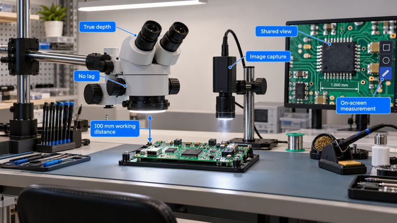
Figure 4: A stereo and a digital microscope set up side by side at a PCB rework bench
Whether an image needs to be shared, saved, or measured, a digital microscope for PCB repairing will be the winner. The operator is sitting upright, and the saved images are recorded with a lot number. The frame rate needs to be kept high for soldering, as lag between the iron and the image makes rework clumsy. The LeicaS9i blurs the line, since it's a stereo microscope with a built-in 10 MP camera.
| Task | Better Choice | Why It Wins | What to Specify |
|---|---|---|---|
| Hand rework of 0402 and QFN parts | Stereo | True depth for tool placement, no lag | 100 mm (3.9 in) or more working distance |
| AOI false-call review on the line | Digital | Fast, upright, image saved per board | 1080p at 60 fps, measurement overlay |
| Defect reports and failure analysis | Digital | Image capture and on-screen measurement | Calibrated measurement software and image export |
| First article sign-off by a team | Digital or hybrid | Several people share the same view | Large monitor with HDMI output |
| Joints under BGA and LGA packages | Neither | Side-view optics reach the outer rows best, and no optics show voids inside a joint. | X-ray inspection instead |
Key Specs: Magnification, Depth of Field, and Working Distance
The size of the land being judged should dictate the magnification used, as indicated in Table 1-2 of IPC-A-610. Provides a scope of inspection for regular work and a referee power used only to confirm a suspect rejection during inspection. The specified power has a tolerance of ±15%, and the pad sizes of the SMD resistor package guide follow behind the examples.
| Land Width | Inspection Range | Maximum Referee | Typical Features at This Size |
|---|---|---|---|
| Over 1.0 mm (39 mil) | 1.5X to 3X | 4X | 0805 and 1206 chip pads, through-hole lands |
| 0.5 to 1.0 mm (20 to 39 mil) | 3X to 7.5X | 10X | 0603 and 0402 pads, 1.27 mm (50 mil) pitch SOIC leads |
| 0.25 to 0.5 mm (10 to 20 mil) | 7.5X to 10X | 20X | 0201 pads, 0.5 mm (20 mil) pitch QFP leads |
| Under 0.25 mm (10 mil) | 20X | 40X | 01005 pads, 0.4 mm (16 mil) pitch QFN lands |
Lighting Solutions for High-Reflectivity PCB Surfaces
At the microscope level, the solder, ENIG gold, and HASL tin all appear like mirrors, and a single light source will produce a white hotspot in each fillet. IPC-A-610 requires a minimum of 1000 lm/m2 (≠ 93 foot candles) and states that a light source of 3000-5000K is best for identifying features and contamination. However, brightness alone is not sufficient, as certain aspects of the image become visible depending on where the light is positioned.
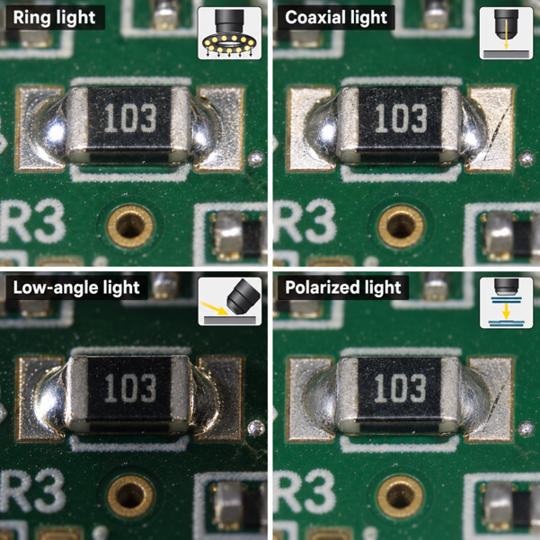
Figure 5: One solder joint under four lighting modes: ring, coaxial, low-angle, and polarized
| Lighting Type | How Light Reaches the Board | What It Reveals | Best Use |
|---|---|---|---|
| LED ring light | Even cone from around the objective | Overall shape of joints, parts, and markings | Every day inspection and rework |
| Coaxial light | Straight down along the lens axis | Scratches, pits, and oxidation on flat pads | Bare copper and ENIG pad checks |
| Low-angle ring light | Grazing light from the side | Raised features such as balls, burrs, and debris | Solder balls, debris, and lifted leads |
| Polarized light | Ring light with crossed filters | Fillet shape without specular glare | Shiny lead-free and HASL fillets |
Advanced PCB Inspection Equipment and Factory Workflows
PCB inspection equipment is located in the factory at three checkpoints: Incoming material, Assembly line, and Final release. Unlike the automated machines, all three types of defects can be caught with a microscope.
IQC: Raw Material and Copper Layer Vbesidesation
Every board is constructed with the material used, and there is an incoming quality control (IQC) test before it goes into production to ensure the material is free of any flaws in the laminate or foil. Copper-clad laminate is checked for pits, dents, scratches, and oxidation. A dent appears as a soft dent in a trace under magnification that will later show up as a thin spot in the trace.
Since the quality of plating is located inside the holes, verification of the copper layer is transferred to a metallurgical microscope. Microsectioning involves potting, grinding, and polishing a coupon from the production panel to reveal a cross-section. The inspector examines the copper hole wall at 100X to 200X magnification for voids and layer separation.
In-Process Hole Wallity Checks During SMT Assembly
SMT assembly inspection is carried out after every step in the process of SMT assembly to find errors, in order to avoid the problem of building on the previous step. Checks are performed in the following order:
- Solder paste inspection (SPI) after stencil printing to measure the volume, height, and offset of solder paste on each pad.
- Checking the value, position, and polarity of all parts per BOM on the first assembled board during first-article inspection.
- AOI after reflow, each part and joint to the reference.
- All AOI calls will be reviewed by a microscope to confirm whether the call is a true defect or a false defect, and will be done by an operator.
The true value of a microscope lies in first-article inspection, where one incorrect reel or one reversed diode would be repeated throughout the run, and the microscope would save money on these. At about 10X, the inspector examines the markings and pin 1 orientation. That check is easier and quicker when silkscreen polarity markings are placed next to each polarized footprint.
Final Quality Assurance Before Shipping
Damage that occurs after the successful completion of the electrical tests is often detected during final quality assurance (FQA/FQC). Boards are removed, cleaned of flux residue, bent pins, and chipped edges, and moved, and scratches on the mask may show up later. A masksl-magnified check focuses on those, according to the IPC class mentioned in the order.
Assembled boards are assembled in accordance with the above IPC-A-610 land-width table, and for bare boards, the IPC-6012 standard requires a routine visual examination at 3 diopters (about 1.75X). If a suspected nonconformance cannot be confirmed to that power, then a higher power (up to 40X) is used. The default high-power inspection results in higher costs but fails to increase reliability, as boards are rejected for cosmetic marks.
Professional Manufacturing Practices for High-Yield PCBs
High-yield results from using optical inspection as a measured process step, not just an informal inspection. It implies standardized standards, standardized and calibrated instruments, and a continuous line of action from each result to the process that produced it.
Integrating Optical Audits into Standard Production Lines
A scheduled, magnified inspection of a sample of boards that already passed the AOI is an optical audit. It determines if the automation is still capturing what it should. Each audit makes the next audit run safer, as every audit that finds a defect the machine missed causes the AOI program to be retuned for that part.
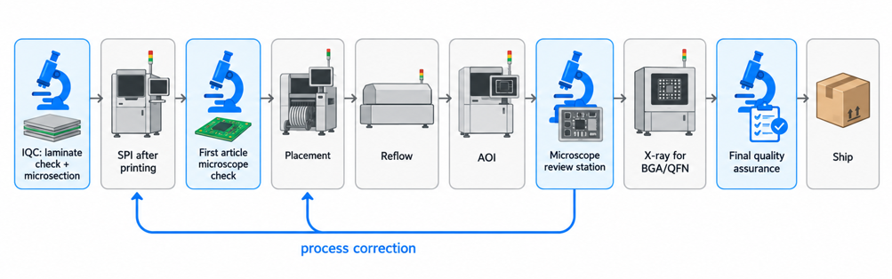
Figure 6: Where optical inspection sits in a PCB production line, from IQC to final release
Digital microscopes offer traceability as each image saved is identified with the board serial number and station. When a field return comes back several months later, the factory can retrieve the original picture. This record helps to differentiate between a manufacturing defect and damage during use.
How Our Rigorous QA Standards Guarantee Zero-Defect Delivery
There is no single inspection technique that can find all defects, so JLCPCB's quality system layers multiple inspections that each find defects that the previous inspection might not. The engineers examine Gerber files before production. AOI then scans the bare board, while flying-probe testing checks it for opens and shorts, and the boards are then subjected to final quality checking, one by one.
The assembled boards are the same as those used in JLCPCB's SMT inspection and testing capabilities. 3D SPI checks paste after printing, and 2D and 3D AOI check placement and soldering. Visual checks are made by trained inspectors on complex structures and customer-specified locations. If you prefer to have these checks printed on your design, upload your Gerber files to the JLCPCB quote page to get a quote instantly.
FAQs about PCB Inspection Microscope
Q: Is a cheap USB microscope good enough for PCB repair?
It is fine for checking 0603 and larger joints after rework. Most low-cost models have a short working distance and a slow frame rate, so soldering under them is awkward. For regular repair, choose a working distance of at least 100 mm (3.9 in).
Q: Can a microscope inspect the solder joints under a BGA?
Mainly the outer rows. A side-view optical system, such as the Ersa ERSASCOPE, looks along the package edge and clearly shows the shape of the outer balls.
Q: Can a digital microscope replace AOI for small production runs?
For a few prototypes, yes, because an inspector can check every joint in a reasonable time. As quantity grows, attention fades, while AOI judges the hundredth board like the first. So lines use AOI to screen and a microscope to confirm.
Q: Why do good solder joints sometimes look defective at high magnification?
High magnification exaggerates normal texture and flux spots. Lead-free solder also cools duller and grainier than tin-lead solder, so that it can pass for a cold joint. A-610 accepts that look, which is why referee magnification is reserved for confirming rejects.
Q: Does a higher-megapixel camera make a better digital inspection microscope?
Not by itself. The lens decides how much detail reaches the sensor, and a 1080p monitor shows only about 2 megapixels. So extra pixels mainly help save stills, while optics and frame rate matter more live.
Conclusion
The PCB inspection microscope isn't a fallback tool for automated inspection because it transforms AOI alerts into decisions and evaluates joint shape to forecast board life. The right choice is after the task: stereo for tasks under the lens, digital for shared images, and magnification adapted to the width of the land.
With packages getting smaller and smaller (01005 chips), more screening will be done in the camera and software. However, borderline joints will be assessed for good optics by an inspector. In the next build, you want a layered inspection; JLCPCB does this from the source of materials to the final release.

Keep Learning
Why PCB Inspection Microscopes Matter in Electronics Manufacturing
Key Takeaways Precise Faults: ICT tests individual components to report exact pin-level failures. Layout-Driven: Coverage relies on test pad size, pitch, and component clearance. Speed vs. Tooling: Bed-of-nails tests in seconds; flying probe requires no custom fixture. Guarded Isolation: Isolates components from parallel paths to catch early defects. Layered QA: Pairs with AOI and AXI for full quality coverage. A PCB inspection microscope earns its place on a production line because the costliest defe......
PCB Delamination Explained: Causes, Detection, and Prevention
Key Takeaways Causes: Moisture turns into steam during 260C reflow, causing layer separation under thermal expansion. Materials: High-temp lead-free builds require mid/high-Tg laminates instead of standard FR4. Detection: Surface blisters are visual, while internal voids need acoustic testing or microsectioning. Prevention: Protect bond strength using balanced copper, proper press profiles, and dry packaging. Fixes: Epoxy repair only works on minor surface defects; internal splits require board replac......
Key Benefits of In-Circuit Test in High-Yield PCB Manufacturing
Key Takeaways Precise Faults: ICT tests individual components to report exact pin-level failures without booting firmware. Layout-Driven: Coverage depends on layout rules like test pad size (0.9-1.0 mm), pitch, and clearances. Fixtures vs. Probes: Bed-of-nails runs in seconds for high volume; flying probes require zero tooling for prototypes. Guarded Accuracy: Guarding isolates components from parallel paths to detect bad values early and lower rework costs. Layered QA: Combining ICT with AOI and AXI ......
Why PCB Test Coupons Are Critical for Reliable Board Manufacturing
Key Takeaways Sacrificial Testing: Coupons allow destructive tests without harming active boards. True Process Mirror: They match the exact stackup and density to reflect panel quality. Clean Measurements: Straight lines enable precise TDR impedance and via inspection. Quality Shield: Coupon failures isolate flawed panels before shipping. A PCB test coupon is the one piece of your order that is intentionally destroyed. It rides in the panel border beside your boards, so it sees every drill, plating, a......
How to Master PCB Impedance Testing for High-Speed Designs
Key Takeaways Verification via TDR: Impedance testing uses Time-Domain Reflectometry (TDR) on test coupons to verify high-speed traces. Real-World Factors: Actual impedance is shifted by manufacturing variables, including trace undercut, solder mask, and pressed dielectric thickness. Design-to-Fab Loop: Use the manufacturer's exact stackup Dk values for layout and TDR reports to refine revisions within $\pm 10\%$ tolerance. An impedance test can be the difference between a USB 3.0 link that works reli......
Guardians of Quality: A Complete Walkthrough of PCB Inspection Standards
Key Takeaways Layered Defense: Combining AOI, AXI, ICT, and FCT covers all inspection blind spots. Paste Printing: Solder paste causes up to 60% of defects, making early checks vital. IPC Standards: IPC Class 3 tightens BGA void limits from 25% to 10%, raising costs. Thermal Balance: Equal layout heating balances reflow pull to prevent tombstoning. Design Control: Clear test pads and visible polarity marks ensure reliable automated checks. PCB inspection is not one check performed at the end of produc......