
Reducing CTE Mismatch Stress: Practical Ways to Build More Reliable PCBs
15 min
- Understanding CTE Mismatch in PCB Materials
- How CTE Mismatch Impacts PCB Performance
- Design Strategies to Minimize CTE Mismatch
- Manufacturing Solutions for CTE Mismatch Control
- JLCPCB's Expertise in Managing CTE Mismatch
- FAQ about CTE Mismatch Stress
Key Takeaways
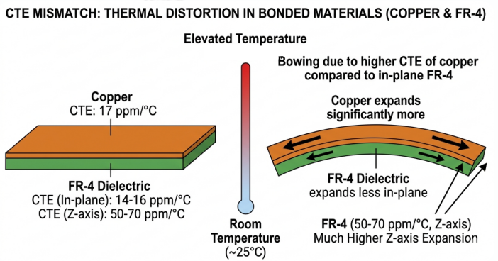
CTE mismatch (FR4’s high Z‑axis CTE vs. copper) creates thermal stress that causes PCB warpage, via cracks, delamination, and solder fatigue—worse under lead‑free reflow and thermal cycling. Mitigate it with symmetric stackups and balanced copper, higher‑Tg/low‑CTE materials, and tight process control (lamination, cooling, moisture, and consistent via plating).
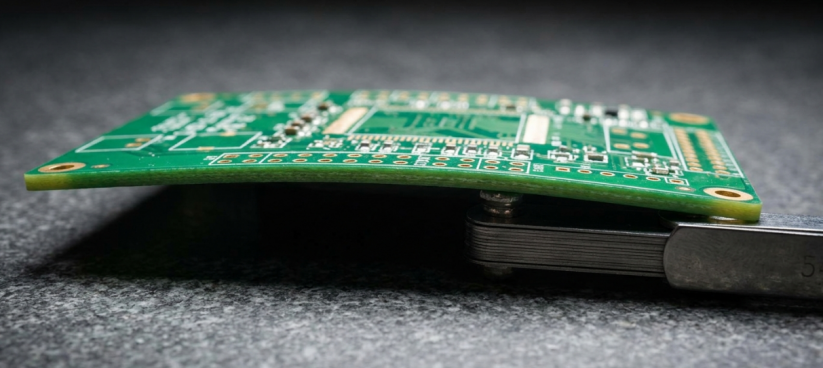
Are you aware that the coefficient of thermal expansion of standard FR4 in the Z-axis can be up to 70 ppm/C, whereas copper has 17 ppm/C only? Four times different is the expansion of these two materials as your board heats. One of the most frequent root causes of warpage, solder joint cracking, and delamination in printed circuit boards is this gap, called CTE mismatch. CTE mismatch was the likely cause of a bowed PCB following reflow, or of the inexplicable barrel cracks in plated through-holes. With thinner boards, smaller components, and higher lead-free reflow temperatures, the management of this thermal expansion difference is more than ever an issue.
Today, we are going to learn what a CTE mismatch is and how it impacts the long-term reliability of your board, and how, in both design and manufacturing, you can ensure that you have it under control. We are also going to examine how contemporary fabricators such as JLCPCB are addressing this issue using sophisticated process controls and material selections.
Understanding CTE Mismatch in PCB Materials
What CTE Mismatch Is and Why It Occurs
All materials are heated to expand and cooled to contract. This behavior is measured by the coefficient of thermal expansion (CTE), which is given in parts per million per degree Celsius (ppm/C). The issue is that a PCB does not consist of one material. It consists of a composite of copper foils, resin-glass laminates, solder, and silicon components, each possessing a CTE value. When two bonded materials do not have the same CTE values, they would desire to increase by varying proportions during a temperature change. This causes mechanical stress internally at the interface since they are physically attached.
Here is a quick look at the CTE values for common PCB-related materials:
| Material | CTE X-Y Axis (ppm/C) | CTE Z-Axis (ppm/C) | Notes |
|---|---|---|---|
| FR4 Laminate | 14-17 | 50-70 | Z-axis CTE drops above Tg |
| Copper | 17 | 17 | Isotropic expansion |
| Lead-Free Solder (SAC305) | 21-23 | 21-23 | Higher than eutectic SnPb |
| Silicon (IC Die) | 2.6-3.1 | 2.6-3.1 | Very low CTE |
| Ceramic (BGA Substrate) | 6-7 | 6-7 | Between silicon and FR4 |
| Aluminum (Heatsink) | 23 | 23 | Isotropic expansion |
| Polyimide (Flex) | 12-20 | 12-20 | Varies with formulation |
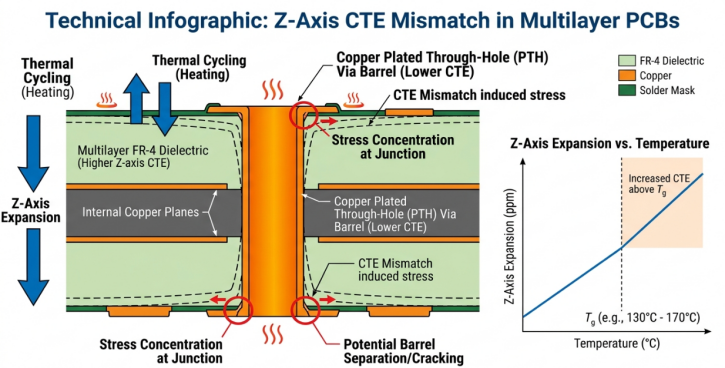
Notice how the Z-axis CTE of FR4 is dramatically higher than its X-Y axis values. This anisotropy is a key factor in reliability failures, particularly for plated through-hole vias that must survive repeated thermal cycling.
Common Effects on Board Warpage and Reliability
A multilayer PCB is reflowed in a reflow oven that reaches a peak temperature of 245-260 °C to solder with lead-free, and each layer expands in its own way. The resin system will soften at temperatures above its glass transition temperature (Tg), and the Z-axis CTE can increase even more. This disproportionate growth brings about a number of apparent and unspoken issues. The most apparent effect is board warpage. IPC-A-600 states that surface mount boards should have a maximum warpage of 0.75%. This implies that a 100 mm board cannot bow more than 0.75 mm. Over CTE mismatch between copper-heavy and copper-light can easily exceed this limit.
Other effects of reliability are:
- Stress on the Z-axis expansion, which causes the plate's through-hole barrel cracks.
- Copper-laminate delamination.
- Pad cratering, in which the resin fractures under BGA pads.
- Repeated thermal cycling of solder joints.
- Cracking of microvia in HDI stackups using laser-drilled vias.
These failures are not always obvious at the moment. They also build up hundreds or thousands of thermal cycles, and thus are particularly unsafe in high-reliability uses such as automotive, aerospace, and medical devices.
How CTE Mismatch Impacts PCB Performance
Thermal Stress, Delamination, and Solder Joint Failures
The predictable pattern of mechanical stress due to CTE mismatch occurs. Bonding two dissimilar materials with differing CTE values and subjected to a change in temperature, the thermal stress that is attained can be estimated based on the change in CTE between the two materials, the change in temperature, and their elastic characteristics. In a simplified example, the difference between the CTEs of the interface multiplied by the temperature change proportions the thermal strain at the interface. In formula form:
Thermal Strain = (CTE1 CTE2) x Delta T.
CTE1 CTE2 Delta T is the change in temperature of the two materials when they are free of any stress. This provides the basic driver and is dependent on the actual stress, which is determined by the geometry, the elastic modulus, and the constraint conditions. Take a BGA part (ceramic substrate (CTE = -7 ppm/C)) on FR4 (CTE = -14-17 ppm/C in X-Y). The change of strain when the temperature varies by 200 °C between room temperature and reflow peak is approximated to be (17 - 7) x 200 = 2000 microstrains. That strain is concentrated in the solder joints, especially those that are nearest to the outside of the ball and therefore the furthest separated by the neutral point.
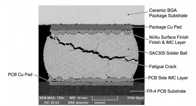
Delamination happens when the interfacial stress is greater than the bond strength between layers. The interface between the copper foil and the prepreg resin is normally the weakest in multilayer PCBs. This is aggravated by moisture absorption since trapped water vapor expands at reflow temperatures very quickly, a phenomenon referred to as the popcorn effect. The failures of solder joints due to CTE mismatch are a result of fatigue. The solder undergoes some plastic deformation in each thermal cycle. With time, microcracks develop and extend until the joint breaks. Coffin-Manson relationship is a relationship that is usually employed to estimate the solder joint fatigue life on the basis of the cyclic strain range.
Calculation Methods and Prediction Tools
Prior to committing to fabrication, engineers can quantify and predict the effect of CTE mismatch in a number of ways. These include the use of basic hand calculations to advanced simulation tools.
- Laminate theory is used to estimate the effective CTE of a multilayer stackup using analytical calculations. Classical Laminate Theory (CLT) considers each layer as possessing known properties and calculates the composite behavior.
- The entire 3D thermal-mechanical response is modeled using Finite Element Analysis (FEA) software such as ANSYS, Abaqus, or Siemens Simcenter. These are able to predict warpage, stress concentrations, and fatigue life.
- Method 2.4.41 of IPC-TM-650 offers a standardized test procedure for determining CTE of laminate materials by Thermomechanical Analysis (TMA).
- Coffin-Manson fatigue models are used to model solder joint life depending on the amplitude of cycles of strain, with modified models including mean stress and creep effects.
Tools that simulate warpage during reflow can be built into EDA platforms to enable designers to identify problem areas at the early stages.
Design Strategies to Minimize CTE Mismatch
Symmetric Stackup and Balanced Copper Distribution
The best solution to CTE mismatch effects is to ensure that your layer stackup is correct at the beginning. A symmetric stackup implies that the arrangement of layers is reflected about the board center. This is to make sure that the forces of thermal expansion on the upper half are counterbalanced by the same forces on the bottom half, which significantly decreases warpage.
This is what a moderate course would have resembled in reality:
- Copy the types of copper layers surrounding the board center (signal-plane-plane-signal on 4-layers, etc.)
- Prepreg type and thickness on the two sides of the center core are the same.
- Compare percentages of copper coverage on pairs of mirrored layers.
- Do not load up one side with heavy ground pour and skimpy routing on the other.
Balancing of copper is also important. When your top is 80% fill with copper, and your bottom is only 20% fill, the board will bow toward the low-copper end as it cools down. The copper-rich side contracts less due to the low-CTE of copper compared to resin, which results in an asymmetric stress distribution. The general rule of thumb is to maintain the copper distribution between the matching pairs of layers at 10-15%. Most EDA tools, such as EasyEDA, allow you to add copper fills to fill in sparse areas. The distribution can be equalized even by non-functional copper pads or hatched fills on inner layers.
Material Selection for Better CTE Compatibility
The appropriate laminate material can greatly minimize CTE mismatch during the initial stages. FR4 is good in most applications, but where thermal reliability is needed, you can do better.
| Material | Tg (C) | Z-Axis CTE Below Tg (ppm/C) | Z-Axis CTE Above Tg (ppm/C) | Best For |
|---|---|---|---|---|
| Standard FR4 | 130-140 | 50-60 | 250-300 | General purpose |
| Mid-Tg FR4 | 150-160 | 45-55 | 200-250 | Lead-free assembly |
| High-Tg FR4 | 170-180 | 40-50 | 180-220 | Automotive, industrial |
| Low-CTE Laminate | 175-200 | 25-35 | 100-150 | High-reliability |
| Polyimide | >250 | 40-55 | 50-60 | Extreme temperature |
| BT Epoxy | 185-210 | 40-50 | 150-200 | IC substrates |
Here, the most important point is Tg selection. Above the glass transition temperature, the Z-axis CTE of FR4 can increase by 4-5 times. In lead-free reflow at 260 °C, a typical Tg 130 board takes a lot of time over its Tg, exhibiting extremely high Z-axis expansion. The higher the Tg of a material, the greater the duration it remains below its transition point during a reflow cycle, minimizing maximum expansion.
Inorganic fillers such as silica or ceramic particles can be added to filled resin systems to reduce the Z-axis CTE to 25-35 ppm/C. These materials are more expensive, but may be needed in thick boards with numerous plated through-holes or numerous-layer-count HDI designs. In the case of designs with a high BGA density, it is advisable to use laminate materials that have a closer X-Y CTE to the component substrate. This decreases the shear stress of solder joints during thermal cycling and increases fatigue life.
Manufacturing Solutions for CTE Mismatch Control
Precision Lamination and Cooling Techniques
Even the best material selection and design practices can be undermined by poor manufacturing execution. The multilayer stackup becomes bonded into a lamination process where heat and pressure are applied, and it is also a critical control point to manage CTE mismatch. In the lamination process, the resin in the prepreg sheets is melted, flows, and cured under pressure. Temperature profile, pressure distribution, and cooling rate all affect the residual stress that is trapped in the completed board. This is what counts the most:
- Even heating of the lamination press means that the whole panel will cure equally. Hot spots bring about localized stress concentrations.
- Regulated pressure application helps to avoid starvation of resin in certain sections and overflow in others. The common lamination pressures are between 200 and 400 PSI based on the material system.
- Optimized cure profiles are done as recommended by the resin manufacturer. Uncured resin is erratic in its CTE performance, whereas over-cured resin is brittle.
- Probably the least considered factor is controlled cooling rates. Quick cooling traps in greater residual stress since the outer layers cool and solidify earlier than the interior layers. The stress is relieved by a gradual, steady decrease in cure temperature to room temperature.
Process Controls to Reduce Residual Stress
In addition to lamination, a number of downstream manufacturing processes can add or alleviate CTE-related stress. It is the ability to manage these processes as a whole that makes the difference between a good board and a marginal board. Drilling causes local heat, which may damage the resin at the wall of the hole. Contemporary CNC drilling machines regulate the speed of the spindle, feed rate, and chip load to reduce thermal damage. When drilling thick boards or small holes, retraction cycles of peck drilling can remove debris and minimize heat accumulation.
The consistency of plating thickness is important since the thick copper in vias should be able to withstand Z-axis expansion without cracking. Class 3 of IPC-6012 mandates 25 micrometers or more copper plating in through-hole barrels. Even plating provides even stress distribution.
Some of the important process controls are:
- The inspection of incoming material in terms of CTE values and Tg verification with the help of TMA.
- Embedded thermocouples in lamination cycles.
- Dimensional stability after lamination according to IPC-TM-650.
- Pre-solder mask baking to relieve moisture and stress.
- Last warpage check according to IPC-A-600 guidelines.
Patterns of thermal relief on copper planes surrounding through-hole pads also contribute. Full connection pads are effective in transferring heat, making them stress concentrators. Thermal relief pads in the form of spokes minimize the temperature gradient during soldering, decreasing the maximum CTE mismatch stress on the barrel.
JLCPCB's Expertise in Managing CTE Mismatch
Advanced Material Options and Process Optimization
In creating the dependable boards that can withstand thermal cycling, the material portfolio and process capability of your fabricator count. JLCPCB provides a variety of laminate products that have been strategically selected to meet the CTE mismatch issues in various applications. Their typical FR4 incorporates mid to high Tg materials that can be lead-free assembled. Their advanced options include high-Tg laminates (Tg 170 °C and higher) and special low-CTE materials, which are required in demanding applications.
The instant quoting system enables you to specify material requirements and view their impact on cost and lead time, to make informed tradeoffs. JLCPCB lamination presses have programmable temperature and pressure profiles, optimized to each material system, on the process side. Their managed cooling routines assist in reducing residual stress in multilayer boards, particularly significant in 6-layer and beyond stackups, where CTE disparities influence across additional interfaces.
Rigorous Testing and DFM Support for Reliable Boards
Managing CTE mismatch needs to be verified and not well-intended. The quality control procedure of JLCPCB involves warpage measurement, cross-sectional analysis of via integrity, and thermal stress testing as per IPC-TM-650 standards on boards that are to be used in high-reliability applications.
Their DFM (Design for Manufacturability) check finds possible CTE mismatch problems even prior to the start of fabrication. This involves: checking on:
- Asymmetric stackup designs that beckon warpage.
- Copper distribution differences between pairs of layers.
- Through aspect ratios that can be susceptible to Z-axis expansion stress.
- Fit with the reflow profile of the given assembly.
This preventive measure spares you the task of finding out about the failure of CTE related to the assembly, at which point the rework or scrap cost is much greater. JLCPCB offers PCB manufacturing, starting at just $2, and assembly options, which allow you to test and test your thermal reliability plan before you commit to large-scale manufacturing.
Proven Results in High-Reliability Production
The history of the company in the automotive, industrial, and consumer electronics industry confirms that JLCPCB can cope with CTE mismatch in various application needs. Their IPC Class 2 and Class 3 processes assure that boards satisfy the reliability criteria that your application requires. The interplay of material mastery, process management, and stringent testing produces a manufacturing environment in which CTE mismatch has become a controlled issue and not a random occurrence.
This degree of fabrication is necessary for engineers with thermally challenging designs. When you are creating boards that will be exposed to extreme thermal conditions or be subjected to thermal cycling, you may want to consider using the advanced material options and DFM review services at JLCPCB early in your design. It is always less expensive and quicker to detect CTE mismatch problems during the design phase than during production.
FAQ about CTE Mismatch Stress
Q: What is a CTE mismatch in PCBs?
CTE mismatch refers to the difference in thermal expansion rates between materials bonded together in a PCB. Since a circuit board is made of copper, resin-glass laminates, solder, and silicon components, each with different CTE values, they expand and contract at different rates during temperature changes.
Q: How do you calculate CTE mismatch stress?
The fundamental calculation starts with the thermal strain formula: Strain = (CTE1 - CTE2) x Delta T, where CTE1 and CTE2 are the expansion coefficients of the two materials and Delta T is the temperature change. The actual stress is this strain multiplied by the effective elastic modulus of the constrained system.
Q: Why is Z-axis CTE more concerning than X-Y axis CTE in PCBs?
The Z-axis CTE of FR4 (50-70 ppm/C) is much higher than its X-Y axis CTE (14-17 ppm/C) because the glass fiber reinforcement constrains expansion in the X-Y plane but not through the thickness. This high Z-axis expansion puts tremendous stress on plated through-hole vias and interlayer bonds, making it the primary direction of concern for reliability failures.
Q: What TG should I specify to reduce CTE mismatch problems?
For lead-free assembly with reflow temperatures of 245-260 °C, a minimum Tg of 150 °C is recommended, with Tg 170 °C or higher preferred for multilayer boards with four or more layers. Higher Tg materials maintain their lower CTE values over a wider temperature range during reflow, reducing peak Z-axis expansion.
Keep Learning
How Modular PCB Design Simplifies Complex Electronics Projects
Key Takeaway Modular PCB design simplifies complex electronics by breaking boards into independent, reusable functional blocks with clear interfaces. It boosts reusability, speeds up debugging, enhances team collaboration, and reduces errors.Shift from flat to modular design for faster development and more scalable, reliable PCBs. Ever seen a 400+ component schematic and got your head scrambled before even beginning routing? You are not alone. With the ever-increasing density of electronics combined w......
Your Ultimate Guide to PCB Rulers
In the world of PCB design and manufacturing, having the right tools is crucial for achieving accuracy and precision. One such tool that has gained popularity among professionals and hobbyists is the PCB ruler. This specialized measuring tool is designed to provide accurate measurements, reference information, and component footprints, assisting designers, engineers, technicians, and assemblers in various stages of PCB development. In this guide, we'll explore what a PCB ruler is, the features and mea......
Understanding the Materials Used in PCBs: Selection, Types, and Importance
Key Takeaways FR-4 is the go-to material for most cost-effective and reliable PCBs. Use Rogers for high-frequency and RF applications to reduce signal loss. Higher copper weight (2oz) improves current and heat handling. Choose High-Tg substrates for better thermal stability in multilayer boards. Green LPI soldermask offers the best balance of performance and inspection. Printed circuit boards (PCBs) are an essential component of modern electronics. These boards connect and support electronic component......
How to Select Tg of PCB ?
What is the Tg of PCB? In PCB manufacturing, "Tg" stands for Glass Transition Temperature. It is the temperature at which the PCB substrate material transitions from a rigid, glassy state to a soft, rubbery state. PCBs are flame-retardant (UL94 V-0) and do not burn easily; instead, they soften above Tg. The Critical Correlation Between Tg and Z-Axis CTE (Coefficient of Thermal Expansion) When the temperature exceeds the Tg point, the PCB substrate material (such as standard FR-4) undergoes a physical ......
How to Choose the Thickness of PCB
First, In the world of electronic products, the PCB is often referred to as the "heart" of the device. It interconnects all components, making board thickness one of the most important parameters. Choosing the right PCB thickness directly affects the electrical performance, mechanical stability, thermal management, and long-term reliability of the final electronic product. The process of selecting PCB thickness is influenced by various factors, such as product application scenarios, board material, an......
PCB Copper Pour Basics
What is Copper Pour in PCB Design? Copper pour refers to the technique of filling unused areas of a PCB's copper layers with solid copper planes. These planes are connected to power or ground nets, creating a continuous conductive path. Copper pour is typically used in the power and ground planes, as well as in signal layers for specific purposes. Purpose and Benefits of Copper Pour: Copper pour is primarily used to fill unused areas on PCB copper layers with solid (or hatched) copper connected to pow......