Why Accurate NPTH Design Matters for Reliable PCB Manufacturing
13 min
- Understanding NPTH Holes in PCB Fabrication
- Key Design Considerations for NPTH Holes
- Manufacturing Challenges and Precision Solutions for NPTH
- Best Practices for NPTH in Complex PCB Projects
- JLCPCB's Professional Capability in NPTH Processing
- FAQ about NPTH Design
- Conclusion
Key Takeaways
- NPTH are mechanical holes (no copper plating) used for mounting, alignment, and tooling.
- Poor NPTH design often causes PCB cracks during assembly or screw tightening.
- Follow key rules: ±0.08 mm tolerance, ≥0.5 mm diameter, 0.2–0.3 mm copper clearance.
- Keep adequate material around edge holes and clearly mark NPTH in fabrication files.
- Proper NPTH design + DFM checks ensure reliability from prototype to mass production.
Ever get a slight crack in a finished PCB when putting it into an enclosure, tightening the screws? That is usually the clue of an NPTH gone wrong, that little sound. A non-plated through hole that is too near copper or a hole slightly off center that is not specified with the correct tolerance can slowly destroy a perfect board. Most engineers spend hours thinking about impedance and decoupling, then they think about mounting holes, last.
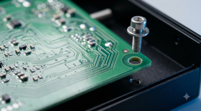
The thing is, those mechanical holes have actual stress; they determine your alignment and how your board will hold up after assembly and field use. The NPTH hole in the PCB is a minor, yet significant factor in determining reliability. This guide will take you through exactly what an NPTH is, how it's different from a plated hole, and the sizing, tolerances, and DFM rules to prevent a failure point. At the end of the course, you will be able to define the NPTH features you would like your fabricator to hit each and every time, from single prototype to full production run.
Understanding NPTH Holes in PCB Fabrication
What NPTH Is and How It Differs from PTH
A Non-Plated Through Hole (NPTH) is a hole drilled completely through the board; there is no copper barrel, no conductive coating, and no electrical function. It is only there for mechanical reasons. A Plated Through Hole (PTH), on the other hand, has a thin electrolytic copper barrel (usually 20-25 µm) covering its walls, which is used to carry a current between the layers or anchor a soldered lead.
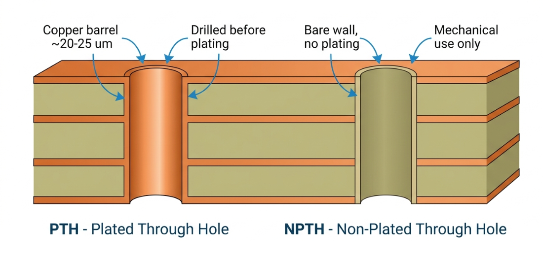
It's more than just plating. The two holes are, in fact, manufactured at different stages of the manufacturing process. PTH holes are drilled early and deposited with both electroless and electrolytic copper plating to make the barrel. NPTH holes are either masked off during plating or, in a second drill step (more common), holes are drilled after plating in such a way that no copper is exposed to the wall. Once one knows the difference between pth and npth, the design implications are clear. These are the factors that most matter, and a comparison between them:
| Factor | PTH (Plated Through Hole) | NPTH (Non-Plated Through Hole) |
|---|---|---|
| Wall plating | Copper barrel (20-25 µm) | Bare laminate, no plating |
| Primary function | Electrical connection between layers, component leads | Mechanical mounting, tooling, alignment |
| Drill timing | Drilled before copper plating | Masked during plating or drilled after |
| Annular ring | Required (copper pad around hole) | None, or an isolated pad with clearance |
| Relative cost | Higher (extra plating steps) | Lower (simpler process) |
| Typical uses | Vias, through-hole leads, connectors | Screw holes, standoffs, fiducials, tooling holes |
Common Applications of Non-Plated Through Holes
NPTH features are the mechanical design's workhorses. You'll find them seldom in a schematic, but almost every board will have at least one. Due to the lack of signal, they are for holding, locating, or protecting. Non-Plated Through Hole is used for:
- Screw, bolt, and standoff mounting holes for attaching the board to an enclosure
- Holes on the panel for manufacturing and assembly tools to ensure accurate panel positioning.
- Alignment holes for mating with pins to position the board for pick-and-place
- An opening through a metal plate that allows a shaft, connector, or fastener to pass through without touching it.
- Slots and cutouts (routed instead of drilled) for connectors, heatsink tabs, or mechanical keying.
Key Design Considerations for NPTH Holes
Size, Tolerance, and Placement Guidelines
The first ever rule is to match your hole to an actual fastener. For an M3 screw, the clearance hole is about 3.2 mm, an M2.5 screw is about 2.7 mm, and so on. If it's too small, the screw won't fit in place; if it's too large, the board may shake, or the screw's head may tear through. Tolerance distinguishes NPTH from PTH in the eyes of the fabricator. NPTH holes are called out at their finished diameter since there is no plating to reduce the finished diameter.
The mechanical NPTH tolerance is typically within the ±0.08mm range, which is sufficient for standard screws and standoffs. You can specify a tighter tolerance for the press fit dowel pin/bearing seat as long as you are sure that the fabricator can maintain it. As important as size is placement. Mounting holes should be spaced away from the edge of the board so that routing will not break out into them, and space should be provided for the head of the screw or footprint of the washer (the mechanical keep-out may be larger than the hole itself).
Interaction with Copper, Solder Mask, and Board Edge
The NPTH is a wall with no drilled hole, and any copper that comes into contact with an NPTH is subjected to mechanical stress and could short out through a fastener. As a rule of thumb, Copper should be kept a nice distance away from the drilled edge, at least 0.2-0.3mm away from the edge, or further if a metal screw head is to be placed on the surface. Solder mask is also different around NPTH. Fabricators often remove the mask from the hole to prevent a ragged mask edge from being created by the drill or router.
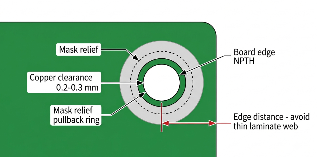
An ordinary NPTH won't make that connection, and if it is designed so that your mounting screw contacts copper (for chassis grounding), you will want a plated hole or a deliberate exposed pad. Extra care is needed for the board-edge NPTH features. If the mounting hole is installed too close to the routed edge, there is a thin, fragile edge of laminate that can crack when depaneling or during screw torque. Provide sufficient material around edge-adjacent holes to maintain integrity.
Minimum NPTH Size and Aspect Ratio Requirements
Each fabricator has a minimum drill size that it is able to run mechanically. The practical lower bound of the NPTH diameter for most typical processes is about 0.5 mm because very small mechanical holes will not gain much and will increase drill-breakage risks. Holes that are smaller in diameter are not NPTH, but plated holes. Even without plating, the aspect ratio (thickness of board divided by hole diameter) will still hold true. A very deep and narrow hole may deviate from the axis or emerge at the other end off-axis. Small mechanical NPTH aspect ratios (below the 10:1 ratio commonly used for plated vias) will provide a straight, clean hole. Thicker boards, in other words, require proportionately larger NPTH diameters to maintain reliability.
Manufacturing Challenges and Precision Solutions for NPTH
Drilling Accuracy, Deburring, and Hole Wall Quality
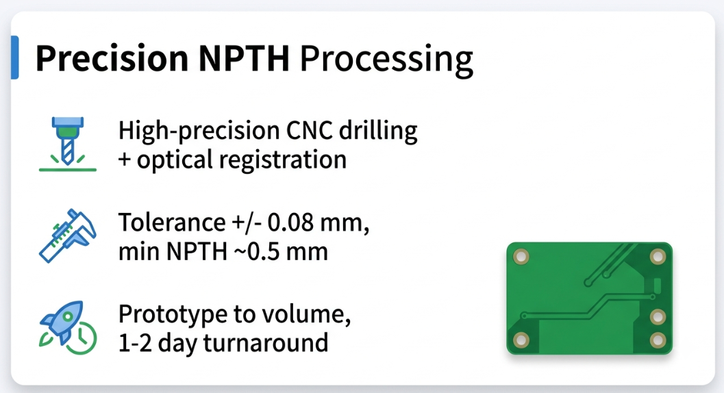
NPTH holes are often drilled separately from the plated holes, creating a registration issue. The second drill pass needs to be aligned to the same datum as the first pass, or it will end up offset from the copper and board outline. This second-drill registration is tightly controlled with high-end CNC drills with optical alignment. The bare laminate walls will also result in burrs and loose glass fibers at the drill exit.
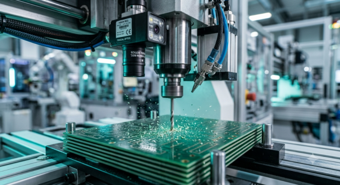
These burrs, if not addressed, will affect screw seating and flatness. The hole edges are cleaned through a proper deburring process (mechanical brushing or a controlled abrasive pass), producing a smooth and dimensionally correct finished feature. Without copper, the wall quality is important. Drill speed, feed rate, and bit sharpness are all optimized for the laminate being cut, and can be affected by rough walls or resin-smeared walls in a press-fit NPTH.
Process Controls to Prevent Common Defects
Most of the NPTH defects are predictable and can be avoided through appropriate controls. These are monitored throughout the job in a well-run fab line.
- Migration of copper into the hole: If the masking does not work during plating, stray copper can show up on the wall, creating an accidental conductor out of a mechanical hole. There are no such problems with robust masking and post-plate drilling.
- Positional drift: Wear on drill bits or lack of registration causes the hole to deviate from the intended location.
- Burrs and delamination: The laminate is cracked around the hole by aggressive feed rates. Optimized parameters of the drill protect edges with optimized entry/exit backing materials.
- Oversized or undersized holes: Bit wear will cause a change in the finished diameter over time. Drift is detected before it exceeds tolerances by statistical spot checking of the drill chart.
Best Practices for NPTH in Complex PCB Projects
Mechanical Strength, Alignment, and Assembly Optimization
Treat all of the mounting NPTH as if it's a load-bearing point. The torque and vibrations will be focused around the screws when a board is screwed down, and the laminate around the screws should have adequate thickness to minimize cracking. A non-functional keep-out ring, copper-free and component-free ring around each mounting hole, helps distribute stress and provides a clean seat for washers. The Alignment holes are considered to be your mechanical reference. Select two NPTH tooling holes that are reasonably far apart to use as datums, and dimension all other critical features from the two, thus establishing a common origin for the board, the enclosure, and the assembly line. This significantly minimizes the misalignment of the stack-up in multi-board or panelized products.
DFM Rules Specific to NPTH Features
NPTH fabrication is predictable with a clean Design for Manufacturability (DFM) package. Embed these rules in your CAD library, and save yourself from a lot of queries from fabricators:
- Clearly mark NPTH in your drill file/fabrication notes, your hole might get plated, and your drill won't fit!
- To prevent shorts and edge stress, keep copper away from each and every NPTH by your fabricator's clearance.
- Limit minimum diameters and do not go below 0.5 mm NPTH. If required, use plated holes for diameters below this.
- Call out reasonable tolerances like ±0.08 mm for standard mechanical holes and only tighten them up if a press fit is needed.
JLCPCB's Professional Capability in NPTH Processing
Advanced High-Precision Drilling and Routing Equipment
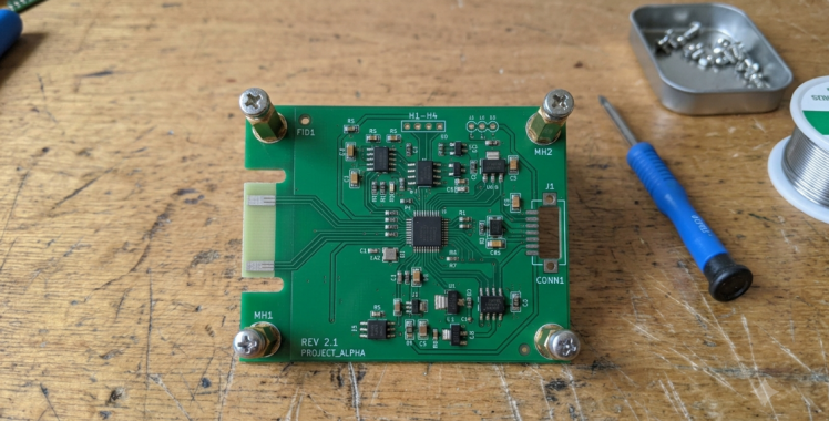
The optical registration is critical for accurate NPTH work, and JLCPCB has modern CNC drilling and routing lines to do so. Camera-aligned positioning ensures that the mechanical holes are registered to the copper and board outline, as often non-plated holes are a separate drill operation. An accurate routing creates not only round holes, but clean NPTH slots and cut-outs.
Strict Tolerance Control and Comprehensive DFM Feedback
Control equals consistency. JLCPCB can achieve mechanical hole tolerances of approximately ±0.08 mm, and can provide NPTH features with a diameter of about 0.5 mm, meeting most mounting and tooling requirements. Equally important, their automated DFM check will alert you to NPTH issues before they enter the manufacturing process, such as copper too close to a mechanical hole, holes too close to an edge, or an accidentally placed mechanical hole set to plate. That feedback loop captures the errors that would otherwise result in thrown-away boards.
Consistent High-Quality Results from Prototype to Volume Production
The true measure of any process is repeatability. Production turnaround is as quick as 1-2 days, and the minimum price of prototype PCBs is about $2, so you can try the NPTH placement in a small batch and then mass produce at the same drill accuracy with the same tolerance control. If you're interested in applying these NPTH principles to your designs, one easy way to get real DFM feedback on your mechanical holes before you commit is to upload them to JLCPCB's instant quoting system.
FAQ about NPTH Design
Q: What is NPTH in a PCB?
NPTH stands for Non-Plated Through Hole, a hole drilled through the board with bare laminate walls and no copper plating. It serves mechanical purposes such as mounting, alignment, and tooling rather than carrying any electrical signal.
Q: What is the main difference between PTH and NPTH?
A PTH (plated through hole) has a copper barrel on its walls to conduct electricity between layers or anchor component leads, while an NPTH has no plating and is purely mechanical. PTH holes are drilled before copper plating; NPTH holes are masked off or drilled afterward so no copper reaches the wall.
Q: What is the minimum NPTH hole size and tolerance?
Most fabricators, including JLCPCB, support NPTH diameters down to about 0.5 mm with a typical finished tolerance of around ±0.08 mm. Because there is no plating, NPTH holes are specified at their final finished size directly.
Q: How much copper clearance should I keep around an NPTH?
Keep copper features clear of the drilled edge by at least about 0.2-0.3 mm, and more if a metal screw head or washer will contact the surface. This prevents accidental shorts, edge cracking, and exposed-copper stress around the mechanical hole.
Q: Can an NPTH be used for grounding a board to a chassis?
Not on its own. A standard NPTH has bare walls and makes no electrical connection. For chassis grounding through a screw, you need a plated hole or a deliberately exposed copper pad designed to contact the fastener.
Conclusion
As it turns out, when it comes to reliability in PCB production, it isn't just about signals and stackups; it's also about the mundane mechanical holes that keep it all together. By choosing the correct fastener for the hole, keeping tolerances to a sensible level, avoiding contact with copper, and observing edge distances, you're making a weak point into a solid mounting plan. Good NPTH design is quiet engineering, and no one should notice it.
With denser boards, smaller enclosures, and a smaller margin for mechanical sloppiness, NPTH is a real competitive advantage. Make these rules a part of your footprints, rely on good DFM feedback, and select a fabricator that has drilling accuracy to match your intentions. If you do that, your NPTH hole in PCB features will work perfectly from the 1st prototype to full-scale production.
Keep Learning
Understanding SMT PCB Boards Technology: An Essential Component of Modern Electronics
Surface Mount Technology (SMT) has changed manufacturing of modern electronics. It has made designs and assembly methods more efficient. Many modern electronics depend on SMT PCB boards, which make it possible for circuit designs to be small and efficient. This is what today's technology needs. This article discuss about many types of SMT PCB boards, their uses, and the best methods for designing and assembling them. 1. What is an SMT PCB Board? Printed circuit boards called SMT PCB boards, use surfac......
How to Choose the Right Prepreg Material for Reliable Multilayer PCB
Have you ever wondered what makes all those copper layers stick to a cross-section of a multilayer PCB? Prepreg material is the answer, and it is of much more importance than most engineers think it is. Choose the prepreg selection wrong, and you are predetermined to delamination, impedance drift, and long-term reliability problems. Prepreg is not only glue. It is a designed composite that determines your dielectric separation, dictates your impedance, affects signal loss, and determines your board be......
Via Filling Explained: Key Techniques, Benefits, and Solutions for High-Performance PCBs
Key Takeaways Via filling completely fills plated through-holes and microvias with epoxy or conductive copper paste, followed by planarization and copper capping (POFV). It eliminates voids, solder wicking, and thermal/mechanical issues while enabling reliable via-in-pad designs. Benefits include superior heat dissipation (up to 8 W/m·K), better signal integrity, higher mechanical strength, and improved assembly yields. JLCPCB provides free non-conductive filling + POFV on 6+ layer boards. Ideal for H......
How Fiducial Markers Guarantee Perfect Alignment in Professional PCB Fabrication
Today, the most sophisticated pick-and-place machine can place a 0.5 mm pitch QFP on its footprint, board after board, thousands of times, and never miss. It is not only a matter of expensive cameras or high-quality servos, but it begins with a little, very small copper dot, simply hanging there in the corner of your PCB. That dot represents a fiducial marker, and without it, even the smoothest SMT line would be laying components in the dark. The unrecognized heroes of automated assembly are the fiduc......
Technical Guidance: Character Design Specifications
To facilitate component assembly, future maintenance, and traceability of PCB manufacturing information (such as manufacturer, production date, batch number, etc.), various character markings are typically silk-screened onto the PCB. These include component designators, polarity marks, test point labels, company logos, and production traceability information. Traditional PCB character silk-screening uses the screen printing process, hence the term “silk-screen characters.” High-definition characters a......
Step-by-Step Guide to the Printed Circuit Board Manufacturing Process
Key Takeaways Core Role: PCBs provide the physical foundation and electrical connections for modern electronics. Multi-Step Process: Manufacturing spans design imaging, substrate creation, inner/outer layer etching, lamination, and surface finishing. Precision & Quality Control: Features micro-drilling (down to 100 µm) for layer connectivity, Automated Optical Inspection (AOI), and final electrical testing. Protection & Finish: Solder masks and surface finishes (e.g., ENIG, HASL) protect copper traces......