How to Achieve Reliable Through-Hole Soldering on PCBs
16 min
- What Is Through-Hole Soldering?
- Through-Hole Soldering Steps for Reliable Connections
- Common Through-Hole Soldering Defects and How to Prevent Them
- What Does Reliable Through-Hole Soldering Require from PCB Manufacturing?
- FAQs about Through-Hole Soldering
- Conclusion
key Takeaways
- Wetting & Fill: Heat the lead, barrel, and planes past melting point with active flux to achieve ≥75% vertical fill.
- Process & Prep: Bake damp boards to prevent blowholes, and match wave, selective, or hand soldering to board volume.
- Defect Prevention: Use thermal reliefs to stop heat-sink cold joints, and limit dwell time to avoid pad lifting.
- DFM & Materials: Size holes to max lead dimensions, keep full annular rings, and choose high-Tg FR-4 for multi-pass durability.
Through-hole soldering is a process that connects a component lead to a PCB by placing the lead into a hole in the board, which is then filled with solder. The completed joint is a full-thickness joint, and connectors, transformers, and large capacitors are joined with a bond that is much more resistant to pull-out and vibration than a surface joint. It also implies that the hole, the pad, and the laminate determine the quality of the joint as much as the soldering itself does.
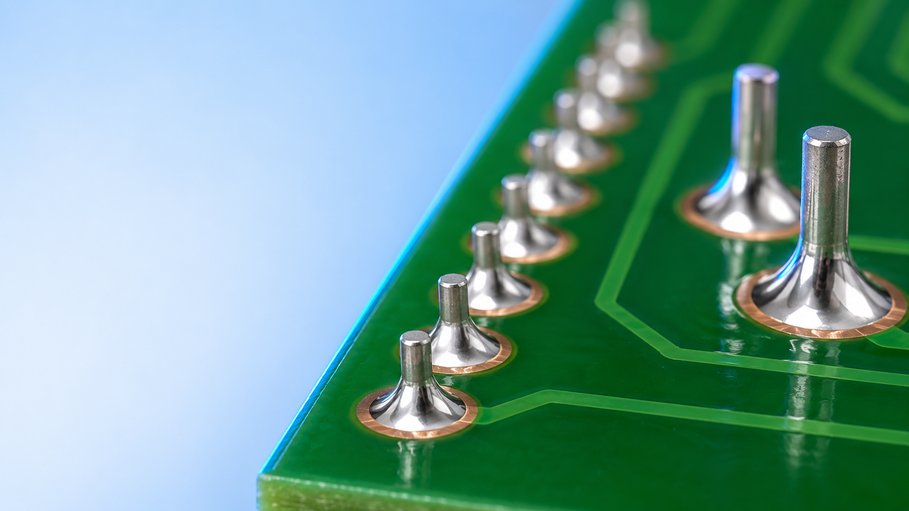
Figure 1: Through-hole leads soldered with concave fillets on the solder side of a PCB
Through-hole joints are formed in this guide, and the techniques of wave soldering and hand soldering are detailed, as are the types of defects that compromise a joint, and the types of PCB features that make a good joint repeatable.
What Is Through-Hole Soldering?
In practice, the term is used to describe any joint in which a component lead passes through the board. The hole can be either plated or unplated, and the solder can be applied by wave, nozzle, or iron. Because it is both a mechanical anchor and an electrical connection, the method has been used consistently in areas where all boards are surface-mount.
How Through-Hole Soldering Works
A plated through-hole (PTH) is a hole that has been drilled and its walls coated with copper plating. The plating connects a pad on the top side with a pad on the bottom side and to any inner layers that the hole traverses. The lead is inserted from the component side, and solder is applied from the solder side. After the molten solder wets the lead and the barrel wall, it is lifted into the gap by capillary action up to the upper pad.
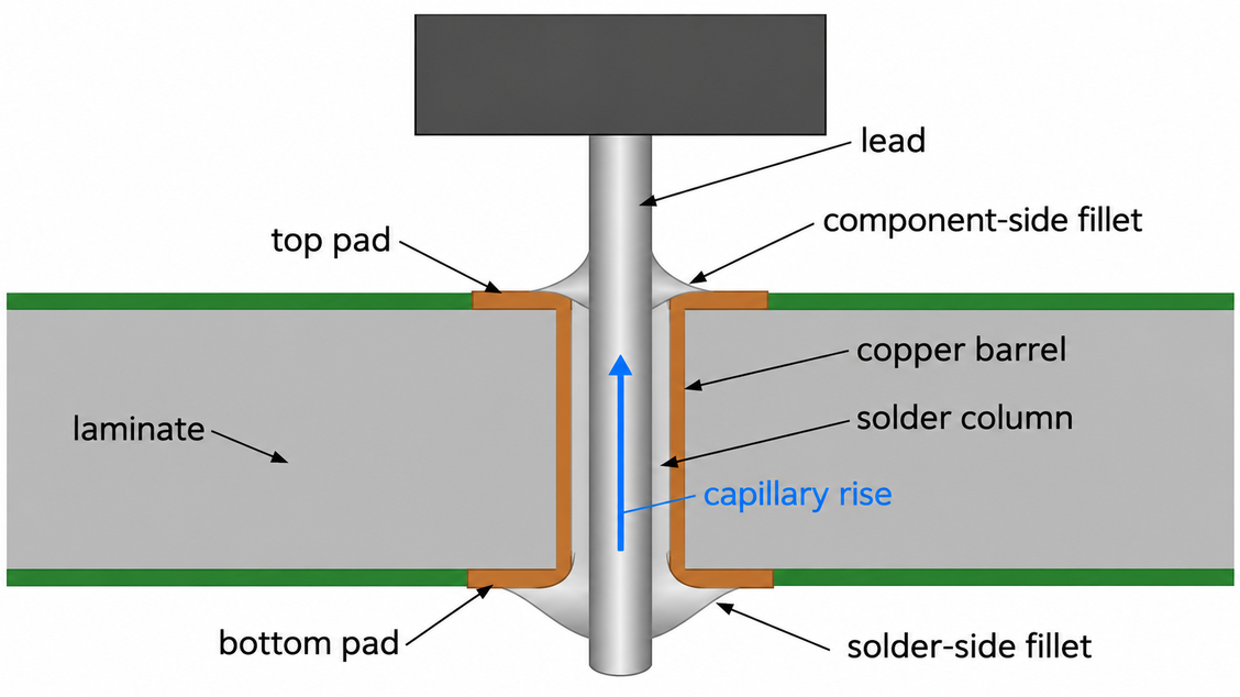
Figure 2: Cross-section of a plated through-hole joint with lead, barrel, and fillets
That increase occurs only in hot, clean sections of the metal. Solder will wet a surface only if the surface is above the solder alloy's melting point and has been cleaned of oxide by the flux. Sn63Pb37 melts at 183 °C, and SAC305 lead-free alloy melts at around 217-220 °C. Thus, the lead, full barrel, and any copper plane attached to the lead all have to pass that point at the same time.
Through-Hole vs. Surface Mount Soldering
Both of these techniques differ in how and where the solder is placed. A surface-mount joint is a joint printed with solder paste and reflowed onto a pad on one surface. A through-hole joint penetrates the board, and solder is applied on the bottom of the board. The SMT parts are reflowed, and a solder wave, a selective soldering nozzle,e or an iron does the job.
| Factor | Through-Hole Soldering | Surface Mount Soldering |
|---|---|---|
| Joint location | Through the board, lead inside a plated barrel | On a surface pad |
| Typical process | Wave, selective, or hand soldering | Paste printing and reflow |
| Mechanical strength | High, resists pull-out and vibration | Lower, relies on pad adhesion |
| Component density | Low, each hole occupies every layer | High, both sides usable |
| Typical parts | Connectors, power parts, heavy or serviceable parts | Most ICs and passives |
Most modern boards mix the two: SMT provides density, while through-hole is reserved for parts that carry mechanical load, handle high current, or require repeated insertion, a trade-off covered in this comparison of SMT vs. through-hole assembly costs.
Through-Hole Soldering Steps for Reliable Connections
A reliable through-hole joint is mostly set up before any solder melts. The work runs in three steps: prepare the holes and leads, apply solder by wave or hand, then inspect and clean the joints.
Prepare PCB Holes and Component Leads
The first step in preparation is to ensure that surfaces are solderable. In storage, pad finishes and component leads oxidize, and flux dissolves only a thin oxide film. Handle and use boards and parts within their shelf life, handling by the edges. If moisture got into the bake boards, bake them to the laminate supplier's bake schedule, as moisture trapped in the bake boards will become steam in the barrel and blow voids or pinholes through the joint.
The leads are then made and installed. Bend axial leads to the hole pitch with a radius, not a sharp corner, at the body, thus not stressing the lead seal. Each lead should go straight through the hole it passes through, and the portion of the lead should be flat or at the indicated standoff. Flux goes on last, from the machine's fluxer or as flux-cored wire plus a flux pen by hand. It must reach the top of the barrel, not just the bottom pad, because solder only climbs as far as the flux has cleaned.
Apply Solder Using Wave or Hand Soldering
The method depends on volume and on what else sits on the board, because each method delivers heat to the joint differently.
| Method | Heat Source | Best For | Main Limitation |
|---|---|---|---|
| Wave soldering | Pumped wave of molten solder under the whole board | Volume boards with many through-hole joints | Bottom-side SMT parts must survive the wave or be shielded |
| Selective soldering | Small solder fountain moved under each joint | Mixed boards with SMT parts near through-hole pins | Slower per joint, needs clearance around each pin |
| Hand soldering | Soldering iron | Prototypes, rework, heat-sensitive parts | Slow, and quality depends on the operator |
Wave soldering runs the board through three zones on a conveyor: a fluxer coats the underside, and preheaters evaporate the flux solvent and warm the board. The underside then crosses a pumped wave of molten solder.
Hand soldering applies the same physics one joint at a time: Touch the tip to both the pad and the lead, and feed solder into the joint on the side opposite the tip. Remove the iron once solder has flowed into the hole and formed a concave fillet, typically within 2-3 seconds. For lead-free wire, a tip setting of about 330-350 °C is a common starting point. A temperature-controlled soldering station with a tip sized to the pad transfers heat more effectively than a higher setting.
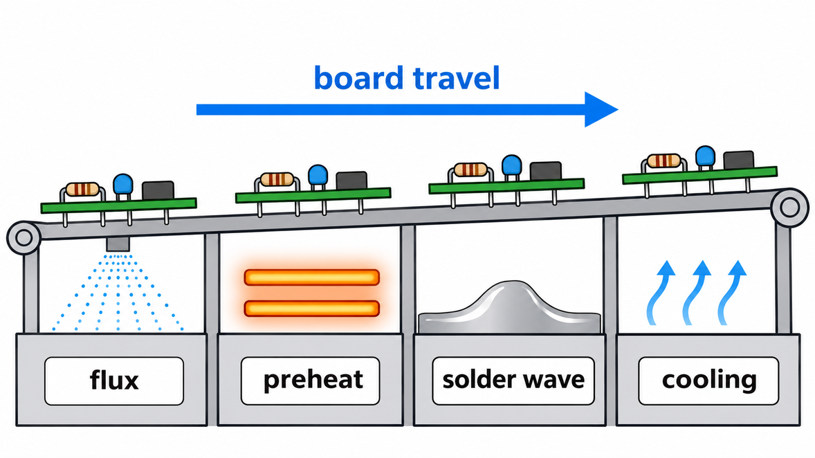
Figure 3: Wave soldering stages: flux, preheat, solder wave, and cooling
Inspect Joints and Remove Residues
Inspection checks wetting, fill, and fillet shape. A good joint wets smoothly to both lead and pad, with a concave fillet and a low contact angle at its edges. Solder should also be visible at the top of the barrel. IPC-A-610 (currently Revision J) and J-STD-001 generally require at least 75% vertical fill for Class 2 and Class 3 assemblies, with limited exceptions for holes tied to heat-sinking planes. When the component body hides the top of the hole, only X-ray inspection can confirm the fill.
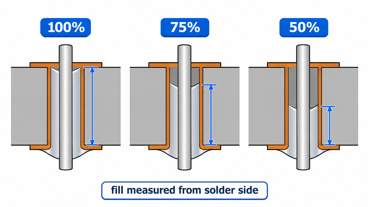
Figure 4: Vertical fill levels of 100%, 75%, and 50% in a plated barrel
Cleaning depends on the flux chemistry. No-clean flux leaves a low-activity residue that is designed to remain on the board, although heavy residue under a connector can still trap moisture. Water-soluble (OA) flux is more aggressive and must be washed off with deionized water, because its residue is corrosive and can grow conductive dendrites between pins under bias. Rosin residue comes off with isopropyl alcohol or a dedicated flux remover.
Common Through-Hole Soldering Defects and How to Prevent Them
Most through-hole defects trace back to heat that did not reach the joint, flux that stopped working, or solder in the wrong place. They fall into three groups: poor hole fill, cold joints and bridges, and heat damage to the pad and barrel.
Insufficient Solder and Poor Hole Fill
Poor fill happens when the solder freezes before it reaches the top of the barrel. The usual cause is heat sinking. A pin tied directly to a ground plane conducts heat away so fast that the top of the barrel never reaches the melting point. A thermal relief connection, a few narrow copper spokes linking the pad to the plane, slows that heat loss while still carrying current. Thick boards and heavy inner copper make the effect worse, so they require more preheat or longer contact time.
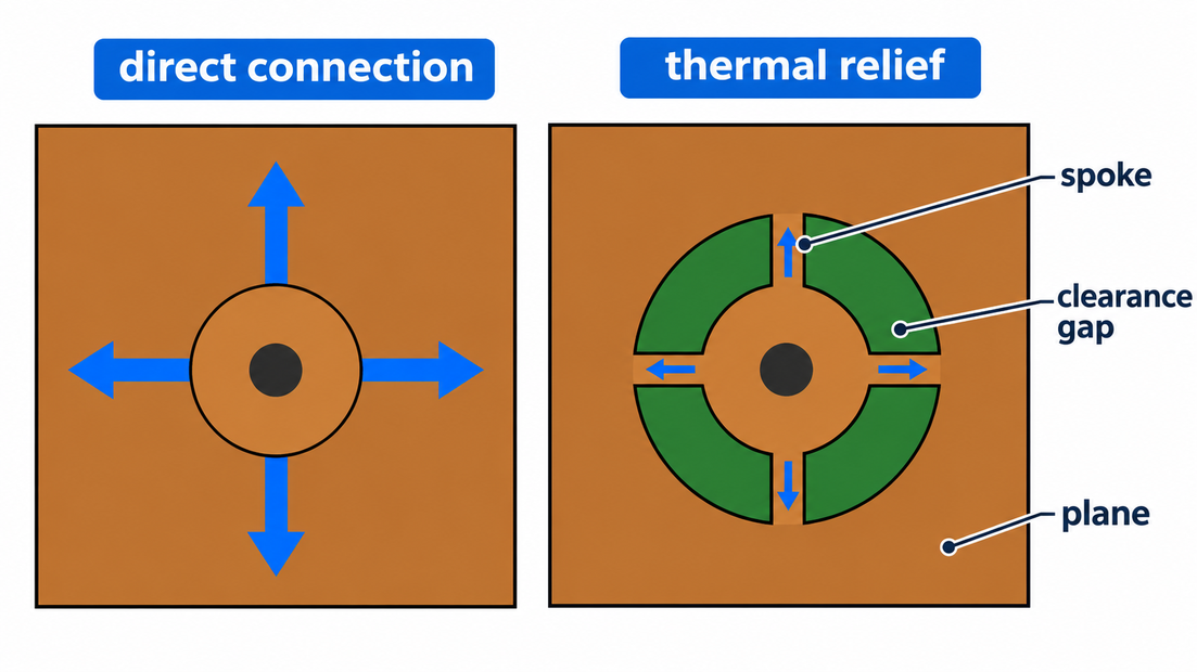
Figure 5: Thermal relief spokes versus a direct plane connection on a PTH pad
Clearance and flux cause most of the remaining cases. A gap that is too tight leaves little room for flux and solder to enter. A gap that is too wide is too large for capillary action to hold the solder column. Low preheat leaves solvent in the barrel to boil through pinholes, while excessive preheat or a slow conveyor exhausts the flux early. The fix is to remove the cause rather than add solder.
Cold Solder Joints and Solder Bridges
A cold joint is solder that melted but never wetted properly: It forms when the lead or barrel stays below the melting range, or when the lead moves as the solder freezes. The joint looks lumpy or grainy and sits on the surface with a convex profile. It can crack within the first thermal cycles. Lead-free joints are naturally less shiny than tin-lead, so judge them by wetting angle and shape rather than luster. Reheating the joint with fresh flux until solder flows into the barrel repairs it.
A bridge is solder that connects two conductors that should be separate: On a wave, bridges form when solder cannot drain off adjacent leads as the board leaves the wave. Spent flux, long leads, and a badly oriented multi-pin part are the common causes. Placing multi-pin parts with their pin rows parallel to the direction of travel helps, because solder then drains toward the trailing pin. In hand soldering, bridges come from too much solder or a tip dragged across pins, and desoldering braid with fresh flux removes them.
Pad Damage and Excessive Thermal Stress
Pad damage usually comes from heat and force together: If the iron is held too long or too hot, it will break the copper/laminate interface bond. If the lead is pulled laterally, the pad is lifted, and each rework cycle further weakens the bond. Plated holes have less tendency to lift than does the unplated pad of a single-sided board, since the barrel holds both pads together through the board.
Thermal stress attacks the barrel itself: The laminate expands several times as much in thickness as copper does, and even more so above the glass transition temperature. Each soldering pass thus extends the barrel plating. Excessive heat exposure may cause it to split down the middle or at the knee where it joins the pad. Lead-free solder will also eat into the copper, causing the barrel to thin out if dwell time is too long or if multiple passes are made. Minimize contact time necessary to obtain fill and minimize rework on the same joint.
What Does Reliable Through-Hole Soldering Require from PCB Manufacturing?
A soldering process can only fill a barrel that was made correctly. Hole size, plating, pad geometry, and laminate, held consistent from panel to panel, decide whether a well-set process gives good joints every time.
Proper Hole Diameter and Plated Through-Hole Quality
Hole size is set from the lead's maximum dimension, not its nominal one. IPC-2222 sizes the minimum finished hole as the maximum lead diameter plus 0.25 mm, 0.20 mm, or 0.15 mm for its producibility Levels A, B, and C. Level A is the easiest to build. A square pin is measured across its diagonal. A 0.64 mm (0.025 in) square header pin has a 0.91 mm diagonal, so 2.54 mm headers commonly use a 1.0 mm finished hole.
The barrel wall must be continuous, smooth, and thick enough to survive soldering. IPC-6012 sets a minimum average hole-wall copper thickness of 20 µm for Class 2 boards and 25 µm for Class 3 boards. Plating voids, nodules, and rough drilling disrupt wetting and leave thin spots that crack first under thermal expansion. Fabricators check these by microsectioning test coupons, and they depend on control of drilling and plating rather than on the layout.
Pad Design and Annular Ring Requirements
The annular ring is the copper between the edge of the hole and the edge of the pad, so pad diameter equals the finished hole plus twice the ring. The ring has to absorb drill position error and still leave a landing for the fillet. Each fabricator publishes its own limits; JLCPCB's for a standard rigid board are:
| Feature | JLCPCB Capability |
|---|---|
| PTH finished hole tolerance | +0.13 / -0.08 mm |
| PTH annular ring, 2-layer, 1 oz | 0.25 mm recommended, 0.18 mm minimum |
| PTH annular ring, multilayer, 1 oz | 0.20 mm recommended, 0.15 mm minimum |
| Pad hole-to-hole spacing | 0.45 mm minimum |
Design to the recommended ring, not the minimum, so the fillet survives a drill that lands off center. For a lead with a maximum diameter of 0.8 mm, Level B yields a 1.0 mm hole. The tolerance then maintains a diametral clearance of 0.12 mm or more, and a 0.25 mm ring yields a 1.5 mm pad. The solder mask opening should cover the entire pad, while a mask strip between closely spaced pins helps prevent bridging.
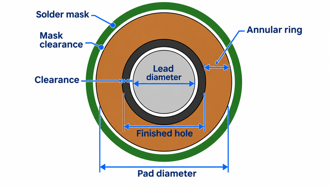
Figure 6: Lead diameter, finished hole, clearance, and annular ring on a PTH pad
PCB Material and Thermal Resistance
The laminate must withstand soldering heat without excessive expansion or delamination. The glass transition temperature (Tg) marks the temperature at which the resin transitions from glassy to soft, which is why the Z-axis expansion rate jumps above it. Isola's 370HR datasheet shows a scale of 45 ppm/°C below its 180 °C Tg and 230 ppm/°C above it, compared with about 17 ppm/°C for copper. A lead-free wave at 255-265 °C takes every FR-4 board well past Tg.
Since every board passes Tg, what separates laminates is the total expansion and the time to delamination at soldering temperature, as listed on datasheets as T260 and T288. Thick boards, multilayers with heavy copper, and boards that see double-sided reflow before wave soldering build up the most time at temperature. For them, a high-Tg FR-4, typically rated at Tg 170 °C or above, lowers the risk of barrel cracks and delamination.
Fabrication Consistency for Reliable Solder Joints
A soldering profile is tuned on a few boards and then run on hundreds of boards, so it only works if every panel matches. Hole size, plating thickness, and solderability finish each affect the heat and wetting a joint needs. A variation the profile was not set for shows up as scattered poor fill or cold joints. HASL and ENIG hold their solderability well. OSP typically degrades with each heat cycle, so an OSP board that has already been reflowed can wet poorly at the wave.
JLCPCB builds rigid boards on Grade A FR-4 from suppliers including Nan Ya, KB, and Shengyi, and lists its drilling and annular ring limits on its PCB capabilities page. Its Economic and Standard PCBA services both support through-hole parts. Unused through-holes are protected from solder during assembly, so they stay open for parts fitted later. With hole and pad sizes matched to those limits, you can get an instant quote for the board and its assemby.
FAQs about Through-Hole Soldering
Q: Is through-hole soldering stronger than surface mount soldering?
Yes, mechanically. The lead passes through the board and is locked by a solder column along the full barrel. The joint therefore resists pull-out, bending, and vibration better than a joint on a surface pad, which is why connectors and heavy parts usually stay through-hole.
Q: Should I use leaded or lead-free solder for through-hole parts?
Use lead-free solder when the product must meet RoHS requirements, and leaded solder only where permitted. Sn63Pb37 melts at 183 °C and wets readily, which makes hand work easier. SAC305 melts at around 217-220 °C and needs more heat.
Q: Does a through-hole joint need solder on both sides of the board?
No. On a plated hole, solder applied from one side flows up the barrel and naturally wets the opposite pad. Soldering the second side separately adds heat but does not improve fill. On an unplated single-sided board, only the copper side is soldered.
Q: Can through-hole components be reflow soldered?
Yes, with pin-in-paste reflow. Solder paste is printed into and around each plated hole, and the leads are pushed through the wet paste. The board then passes through the same reflow oven as the SMT parts, so the component body must be rated for reflow temperatures.
Q: How do you remove a through-hole component without damaging the pad?
Melt all the solder in the barrel before moving the lead. Add fresh solder and flux to improve heat transfer, then clear the hole with a desoldering pump, braid, or vacuum desoldering iron. Pulling a lead from a partly solid joint is what tears pads and barrels.
Conclusion
Reliable through-hole soldering comes down to one rule: heat the lead, the barrel, and every connected plane past the melting point, with active flux, in a barrel the solder can fill. Size holes from the maximum lead dimension, relieve plane connections, and keep annular rings at the recommended value. Choose a laminate for the total heat the board will see. Then set the preheat and contact times based on the flux and alloy datasheets, and verify the fill rather than adding solder.
When your layout is ready, order your PCBs and assembly from JLCPCB, with hole and pad sizes matching its published capabilities.
Keep Learning
Step-by-Step Guide to the Printed Circuit Board Manufacturing Process
Key Takeaways Core Role: PCBs provide the physical foundation and electrical connections for modern electronics. Multi-Step Process: Manufacturing spans design imaging, substrate creation, inner/outer layer etching, lamination, and surface finishing. Precision and Quality Control: Features micro-drilling (down to 100 μm) for layer connectivity, Automated Optical Inspection (AOI), and final electrical testing. Protection and Finish: Solder masks and surface finishes (e.g., ENIG, HASL) protect copper tr......
How to Achieve Reliable Through-Hole Soldering on PCBs
key Takeaways Wetting & Fill: Heat the lead, barrel, and planes past melting point with active flux to achieve ≥75% vertical fill. Process & Prep: Bake damp boards to prevent blowholes, and match wave, selective, or hand soldering to board volume. Defect Prevention: Use thermal reliefs to stop heat-sink cold joints, and limit dwell time to avoid pad lifting. DFM & Materials: Size holes to max lead dimensions, keep full annular rings, and choose high-Tg FR-4 for multi-pass durability. Through-hole sold......
Technical Guidance: Character Design Specifications
To facilitate component assembly, future maintenance, and traceability of PCB manufacturing information (such as manufacturer, production date, batch number, etc.), various character markings are typically silk-screened onto the PCB. These include component designators, polarity marks, test point labels, company logos, and production traceability information. Traditional PCB character silk-screening uses the screen printing process, hence the term “silk-screen characters.” High-definition characters a......
Via Filling Explained: Key Techniques, Benefits, and Solutions for High-Performance PCBs
Key Takeaways Via filling completely fills plated through-holes and microvias with epoxy or conductive copper paste, followed by planarization and copper capping (POFV). It eliminates voids, solder wicking, and thermal/mechanical issues while enabling reliable via-in-pad designs. Benefits include superior heat dissipation (up to 8 W/m·K), better signal integrity, higher mechanical strength, and improved assembly yields. JLCPCB provides free non-conductive filling + POFV on 6+ layer boards. Ideal for H......
How Fiducial Markers Guarantee Perfect Alignment in Professional PCB Fabrication
Today, the most sophisticated pick-and-place machine can place a 0.5 mm pitch QFP on its footprint, board after board, thousands of times, and never miss. It is not only a matter of expensive cameras or high-quality servos, but it begins with a little, very small copper dot, simply hanging there in the corner of your PCB. That dot represents a fiducial marker, and without it, even the smoothest SMT line would be laying components in the dark. The unrecognized heroes of automated assembly are the fiduc......
PCB Via Filling and Covering: Types, Methods & Applications
Key Takeaways PCB via covering and filling are five distinct treatments—untented, tented, plugged, epoxy-filled, and copper-filled—each with different cost, reliability, and thermal trade-offs. Tenting is the default and lowest cost, but can show via yellowing; plugging fills the hole to prevent solder wicking and yellowing. Epoxy-filled and copper-filled vias enable via-in-pad with a flat, capped surface for BGA fanout and HDI designs; copper filling adds high thermal conductivity for power devices. ......