
How Plated Through Hole Technology Creates Reliable Multilayer PCB Connections
14 min
- The Fundamental Role of Plated Through-Hole in Multilayer PCBs
- Key Steps in the Plated Through Hole Process
- Design Considerations for Optimal Plated Through Hole Performance
- Manufacturing Challenges and Professional Solutions
- JLCPCB's Expertise in Plated Through-Hole Fabrication
- Conclusion
- Frequently Asked Questions (FAQ)
Have you ever wondered how a multilayer PCB achieves the feat of holding all the layers together? You can add four, eight, or even twenty copper layers, but unless you have a sure method of connecting the signals between the copper layers, it is just a very expensive paperweight. The plated through-hole is that dependable relation, and it has been the workhorse of multilayer PCB fabrication for a long time. We can take examples from a two-layer Arduino shield to a 16-layer server motherboard; plated through-hole technology is silently working on nearly every board you handle.
It not only provides copper-lined tunnels to make your signal travel between layers to the next, but also provides strong mounting barrels to hold your through-hole components. I am going to take you through the whole process of the plated-through-hole today, i.e., drilling to the final plating. I will also explore the design guidelines that make your vias dependable, examine typical manufacturing glitches, and demonstrate how the newest fabricators, such as JLCPCB, maintain a strict grip on each process.
The Fundamental Role of Plated Through-Hole in Multilayer PCBs
What Plated Through Hole Is and Why It Matters
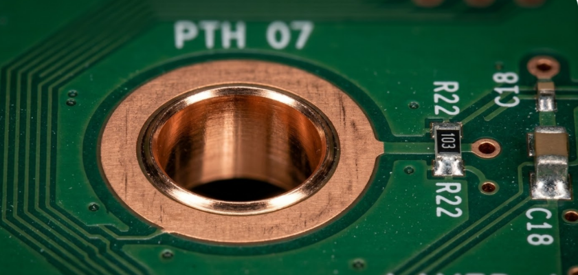
A plated through hole (PTH) is a hole that has been drilled through a printed circuit board and electroplated with copper all around its barrel wall. The mere mechanical hole is transformed by that thin copper lining into a trusted electrical conduit by linking copper traces and copper planes on each side of the hole.
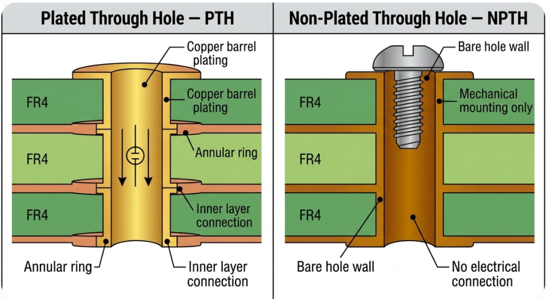
PTH has two different functions. Firstly, it offers mounting sites to through-hole technology (THT) elements like connectors, electrolytic capacitors, and power transistors. Second, it can be used as an interlayer connection and routing signals, power, and ground in multilayer stackups. One should differentiate PTH and a non-plated through hole (NPTH). An NPTH is not copper-plated on its barrel wall, and has no other mechanical function than board mounting or centering. IPC-6012 provides a minimum of 20-25 um average copper plating thickness in a PTH barrel in Class 2 and Class 3, respectively. The sizes of standard drills are between 0.2mm and 6.35mm.
Evolution from Single-Layer to Complex Multilayer Designs
The technology of PTH dates back to the 1940s, when the first PCBs were single-sided phenolic laminates. By the 1960s, there had been the emergence of the double-sided boards, and engineers had to find a method of connecting traces on both sides. The plating was done on holes, which had been made by a relatively crude chemical deposition. Four-layer stackups were developed in the 1980s, and nowadays, HDI designs are routinely produced with 20 or more layers.
The basic PTH process has been the same throughout the generations: pierce a hole, add some electroless copper to it, and electrolytically grow the thickness. In modern HDI boards, standard PTH is enhanced by the use of blind vias, buried vias, and laser-drilled microvias (usually 0.05 mm to 0.15 mm). However, traditional plated through holes are still the workhorse of full-stack connections. Current CNC drilling machines can meet positional accuracy of 0.025mm, and PTH can now co-exist with more sophisticated via structures.
Key Steps in the Plated Through Hole Process
Drilling, Desmear, and Electroless Copper Deposition
Therefore, high-speed CNC drilling will be the beginning of the plated-through-hole process. Carb micro-drill bits are produced by modern machines at 80,000 to 300,000 RPM, and in fact, a hole is punched completely through the entire laminate stack. The speed of the spindle, the feed rate, and the condition of the bit are maintained at a very tight level since a slip can result in a coarse hole wall or smearing of the resin.
Once the hole has been drilled, the walls of the hole absorb a thin layer of epoxy resin due to heat friction. The smear must be wiped off, or the copper plating will not stick to the inner layers. The permanganate desmear method is the go-to method with a concentration of 55 to 85 g/L KMnO4. Etchback is set to 0.5 - 3.0mils, and cuts the resin slightly beyond the copper surface to form a three-point contact that enhances the bond between the layers.
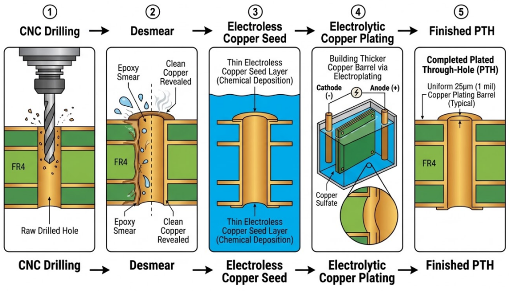
With clean hole walls exposed, the board enters the electroless copper deposition line:
1. Conditioning: A conditioner wets the hole wall and promotes uniform catalyst adsorption.
2. Micro-etch: A mild etch roughens existing copper surfaces to improve adhesion.
3. Pd/Sn catalyst activation: A colloidal solution (100 to 300 ppm Pd) deposits catalytic nuclei on the non-conductive hole walls.
4. Accelerator: Removes the tin shell from the Pd/Sn colloid, exposing active palladium sites.
5. Electroless copper bath: An autocatalytic solution deposits a thin copper layer of 0.5 to 2.0 micrometers on the hole wall.
Electroplating and Thickness Control for Durability
Then you drop the board in the copper plating bath of platinum and electrolyte after you have done the seed layer. The standard acid copper sulfate tank contains approximately 60-80g/L of dissolved copper and 180-220g/L of sulfuric acid, and a current density of 1.5-3.0A/dm 2. In that case, you are getting approximately 25 micrometers of copper an hour. The most difficult thing is to get a copper flat in the barrel. The idea behind throwing power is that it informs you of the goodness with which the solution causes copper to flow into the center of the hole as compared to the rim. Brighteners are important- they accelerate deposition in recessive areas. Levelers reduce the rate of high current spots, and carriers manipulate the grain structure.
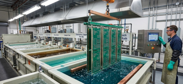
You will find people choosing between panel plating, which is where the entire board is plated simultaneously, and pattern plating, in which a pattern is plated with a photo-resist pattern, and only afterwards are the features plated. In the case of those long, narrow holes, pulse or reverse-pulse plating is more significant since it alternates the current periodically, plating copper deeper into the barrel. Mostly, quality control is based on micro-sectioning and measure the thickness of the copper under a microscope. Then the samples are heated to 288 degrees Celsius and left to run for 10 minutes, as in the IPC-TM-650 test, to ensure that the plating can withstand reflow.
Design Considerations for Optimal Plated Through Hole Performance
Aspect Ratio, Hole Size, and Annular Ring Rules
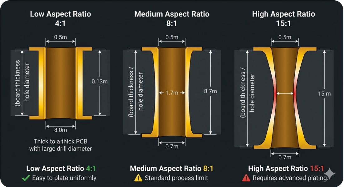
The aspect ratio of a plated through hole is the ratio of board thickness to finished hole diameter. This single number has an outsized impact on manufacturing difficulty. A 1.6 mm thick board with a 0.3 mm finished hole has an aspect ratio of about 5.3:1, well within standard capability.
| Category | Aspect Ratio | Typical Application |
| Standard | Up to 8:1 | Consumer electronics, general-purpose boards |
| Advanced | 10:1 to 12:1 | Telecommunications, networking equipment |
| Specialized | 15:1 to 20:1 | Backplanes, thick aerospace boards |
The annular ring is the copper pad surrounding the drilled hole. IPC Class 2 and Class 3 require a minimum of 0.05 mm, but best practice recommends 0.125 to 0.15 mm for manufacturing margin. The pad size formula is: Pad Diameter = Finished Hole + (2 x Annular Ring) + Drill Tolerance. Anti-pad clearance in internal planes should be at least 0.2 mm.
Integration with Layer Stackup and Via Types
A standard plated through hole passes through every layer. While fine at lower frequencies, the unused barrel portion (the via stub) becomes a signal integrity concern at higher data rates. The stub acts as an unterminated transmission line that creates resonances and degrades the signal path. For designs above 3 to 5 GHz, back-drilling removes the stub. A controlled-depth drill pass from the far side removes unused barrel copper, improving insertion loss by several dB at multi-gigahertz frequencies.
| Via Type | Drill Method | Diameter Range | Layers Connected |
| Standard PTH | Mechanical CNC | 0.2 - 6.35 mm | All layers (full stack) |
| Blind Via | Mechanical or laser | 0.1 - 0.3 mm | Outer to inner layer |
| Buried Via | Mechanical CNC | 0.15 - 0.3 mm | Inner to inner layer |
| Microvia | Laser (UV or CO2) | 0.075 - 0.15 mm | Adjacent layers only |
Via-in-pad technology places the via directly inside the component pad, essential for fine-pitch BGAs. The via is copper-filled and cap-plated to create a flat, solderable surface. Thermal relief pads use narrow spoke connections instead of a full flood, preventing the plane from wicking away too much heat during soldering.
Manufacturing Challenges and Professional Solutions
Plating Uniformity and Void Prevention
I believe that one of the greatest obstacles we continue to stumble upon in PTH fabrication is the ability to have the copper run even around the edge of the hole, all the way to its centre. The density of current is more at the entrance, and the copper is thus likely to be deposited faster there, which also forms an hour-glass shape, where the centre is 40-60% finer than the ends.
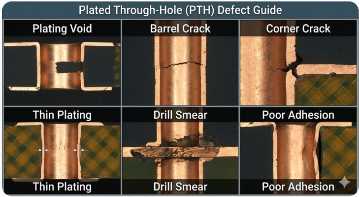
Beyond thickness variation, several defect types can compromise reliability:
- Plating voids: Gaps caused by insufficient catalyst, trapped air, or contamination.
- Corner cracks: Fractures at the barrel-to-inner-layer junction from CTE mismatch stress.
- Barrel cracks: Circumferential cracks from excessive Z-axis laminate expansion during soldering.
- Wedge voids: Triangular voids at inner-layer connections from inadequate desmear or etchback.
The root cause of many thermal failures is the CTE mismatch between FR-4 (Z-axis CTE of 50 to 70 ppm/C above Tg) and copper (about 17 ppm/C). During reflow peaking at 260 degrees Celsius, the laminate expands far more than the copper barrel, placing enormous tensile stress on the plating. IPC Class 3 requires no void exceeding 5 percent of barrel length.
Ensuring Reliability Through Advanced Process Controls
Professional fabricators address PTH challenges through a comprehensive quality system. It begins with material qualification, where incoming laminate, copper foil, and chemistry are tested before production. Drill bit monitoring tracks hits per bit and replaces tools before they degrade hole quality.
Key in-process tests include:
- Microsectioning: Cross-section analysis to measure copper thickness at multiple points.
- Backlight inspection: High-intensity light through the hole to detect voids and cracks.
- Electrical testing: Continuity and isolation testing of every net on the finished board.
- Interconnect stress testing (IST): Accelerated thermal cycling for long-term reliability prediction.
Full lot traceability links every board to its raw materials, drill programs, and plating bath conditions. Statistical process control (SPC) with a target Cpk greater than 1.33 catches drift before it becomes a defect.
JLCPCB's Expertise in Plated Through-Hole Fabrication
Precision Equipment and Tight Process Control
Thus, when JLCPCB is literally implementing those PTH concepts on a large scale, they are operating these high-speed CNC drilling machines that can achieve positional accuracy as low as +/- 0.025 mm, and the drill bit can be as small as 0.15 mm. Their entire desmear and plating process is automated, and it maintains the same chemical concentrations on each of the individual boards coming out of the line.
They are capable of aspect ratios up to 10:1 and beyond, and thus, whether you are working with a single-layer board or a 20-layer stackup, they have the technology to do it. Micro-section analysis, in-line monitoring, and electrical tests are used to ensure that all plated through holes are hitting the IPC-6012 specification each and every time.
DFM Support for High-Yield Multilayer Boards
The best thing about JLCPCB is probably that they have this free online Design for Manufacturability (DFM) tool. Simply drop your Gerber files into the system, and the system will warn you of any typical PTH problems, such as aspect ratios that are too large to fit into their standard configuration, annular rings that are too small to drill reliably, or holes that are larger than the range of those supported by the system.
They also release good design rules that provide a clear guideline on the hole sizes, pad size,s and clearances that should be consistent with their process. That feed-forward is the first thing to have, and before you even get to production, it saves a lot of time and money.
Consistent Quality from Prototypes to Volume Production
One of the biggest victories is that the manufacturing lines are the same when dealing with your prototypes and your final run. It implies that the quality that you test when prototyping is the quality that you will have when you are in volume, no special prototype line or different chemistry that may confuse things.
Two-layered PCBs may often be shipped within as little as 24 hours, and multilayer boards can take between 3 and 5 days. The cost is around two dollars in a batch of five pieces of a standard two-layered prototype, and it becomes quite feasible to test your PTH layout before you have to invest in a large order.
Conclusion
The tech of plated-through-holes may not receive an equal portion of hype as microvias or HDI stack-ups, but it is the real staple of PCB manufacturing. Since CNC drilling and desmearing, electrolytic build-up, and electrolytic seeding all interfere with the efficiency and longevity of the circuit. Understanding the in and out of aspect ratios, annular rings, plating uniformity, and the IPC rules provides you with the know-how to produce boards that actually print clean.
As the designs increase in the number of layers, the game of standard PTH, blind/buried vias, and microvias becomes even more constrained. Get the fundamentals right and nail a good plated hole design, and you have laid the foundation for the rest. When you are willing to put these ideas to the test, JLCPCB has the gears to do it, with its line of gear consisting of precision machines, automated DFM checks, a nd consistency in the quality of production, making it a stroll between drawings and solid hardware.
Frequently Asked Questions (FAQ)
Q1: What is the difference between a plated through hole and a non-plated through hole?
A plated through hole (PTH) has copper plating on its barrel wall, providing electrical connectivity between PCB layers. It is used for interlayer signal routing and through-hole component mounting. A non-plated through hole (NPTH) has no copper on its barrel and serves purely mechanical purposes, such as board alignment.
Q2: What is the minimum copper plating thickness required in a plated through hole?
Per IPC-6012, the minimum average copper plating thickness in the PTH barrel is 20 micrometers for Class 2 (dedicated service electronics) and 25 micrometers for Class 3 (high-reliability applications such as aerospace and medical).
Q3: What aspect ratio can be achieved with plated through-hole technology?
Standard processes handle up to 8:1. Advanced processes using optimized chemistry and pulse plating achieve 10:1 to 12:1. Specialized fabricators can reach 15:1 to 20:1 for thick backplanes and aerospace boards.
Q4: What causes plating voids in plated through holes, and how are they prevented?
Common causes include insufficient catalyst activation, trapped air bubbles, surface contamination, and inadequate desmear, leaving resin residue. Prevention involves thorough desmear processing, proper agitation during plating, and current density optimization for the specific hole geometry.
Q5: How does plated through-hole technology differ from microvia and via-in-pad technology?
Standard PTH passes through all layers using mechanical CNC drilling (0.2 mm minimum). Microvias are laser-drilled (0.075 to 0.15 mm) and connect only adjacent layers. Via-in-pad places the via inside the component pad, copper-filled and cap-plated for a flat solderable surface essential for fine-pitch BGAs.

Keep Learning
Why Accurate NPTH Design Matters for Reliable PCB Manufacturing
Key Takeaways NPTH are mechanical holes (no copper plating) used for mounting, alignment, and tooling. Poor NPTH design often causes PCB cracks during assembly or screw tightening. Follow key rules: ±0.08 mm tolerance, ≥0.5 mm diameter, 0.2–0.3 mm copper clearance. Keep adequate material around edge holes and clearly mark NPTH in fabrication files. Proper NPTH design + DFM checks ensure reliability from prototype to mass production. Ever get a slight crack in a finished PCB when putting it into an enc......
How to Design and Manufacture Reliable Slot Holes in PCBs
Key Takeaways Slot holes are elongated openings ideal for flat pins, connectors, shields, and board alignment. Minimum sizes: 0.5 mm (plated) and 1.0 mm (non-plated); prefer rounded ends with length ≥ 2.5× width. Maintain proper annular ring, edge clearance, and DFM rules to prevent breakout and plating issues. Use overlapping drills for short plated slots and routing for longer ones. Good slot design greatly improves mechanical strength, thermal performance, and assembly reliability. JLCPCB’s precisi......
How Beveled Edges Improve Reliability and Performance in Card Edge Connectors
Key Takeaways Beveled edges enable smooth insertion and protect gold fingers from wear in card edge connectors. Use 30° or 45° angles (45° is standard for most designs) with depth of 1/3 to 1/2 board thickness. They reduce insertion force, prevent plating damage, and improve long-term contact reliability. Proper beveling is critical for high-cycle applications like DDR modules and PCIe cards. Bevel edges came into my attention the first time a memory module that I designed scratched its own gold finge......
How to Prepare Perfect Gerber Files for Flawless PCB Production
Key Takeaways Use RS-274X format and consistent millimeter units for all files. Always include complete layers: Copper, Solder Mask, Silkscreen, Board Outline, and NC Drill. Check your Gerbers in a viewer before uploading to catch errors early. Follow DFM rules: proper annular rings, solder mask expansion, and trace spacing. Use clear file naming and detailed fabrication notes. After spending weeks working on the perfect board layout, the routing is clean, the DRC passes, and you hit “export.” Two day......
Technical Guidance: V-Cut Panelization Standards
For boards with regular rectangular shapes, V-cut (V-scoring) panelization is an efficient method. This process involves cutting V-shaped grooves of a specific depth on both sides of the panel along the board boundaries, leaving a thin web of material (typically about 1/3 of the board thickness) that allows easy manual separation after SMT assembly. After separation, minor thread-like fibers or rough edges may remain and can be lightly scraped off. Due to material expansion and cracking during depanel......
Technical Guidance: Character Design Specifications
To facilitate component assembly, future maintenance, and traceability of PCB manufacturing information (such as manufacturer, production date, batch number, etc.), various character markings are typically silk-screened onto the PCB. These include component designators, polarity marks, test point labels, company logos, and production traceability information. Traditional PCB character silk-screening uses the screen printing process, hence the term “silk-screen characters.” High-definition characters a......