PCB Depaneling for Cleaner Edges and Reliable Production
16 min
- What Is PCB Depaneling and Why Does It Matter?
- Comparing the Three Main PCB Depaneling Methods
- How to Select the Best Depaneling Method for Your PCB
- PCB Depaneling Starts with Manufacturing-Ready Panel Design
- How JLCPCB Supports Reliable PCB Manufacturing
- FAQs about PCB Depaneling
- Conclusion
Key Takeaways
- Timing: Depaneling happens post-soldering, putting stress directly on finished parts.
- Methods: Choose V-cut for straight high-volume boards, mouse-bites for irregular shapes, and lasers for stress-free precision.
- MLCC Safety: Keep parts $\ge$ 1.0 mm from V-cuts, align MLCCs parallel to break lines, or add relief slots.
- Panel Limits: Cap assembly panels at 250 × 250 mm with 5 mm rails, 2 mm tooling holes, and 1 mm fiducials.
- File Prep: Mark "V-CUT"/"CNC" on the outline layer, keep copper clear ($\ge$ 0.4 mm / 0.2 mm), and build stencils from final engineering files.
PCB depaneling is the process of separating individual circuit boards from the production panel on which they were fabricated and assembled. Small boards go through etching, plating, paste printing, and reflow as one large panel, because that is faster and keeps them rigid on the line. At the end, the panel has to come apart, and how it does so determines the edge finish, the outline tolerance, and whether ceramic parts near the edge survive.
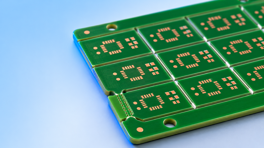
Figure 1: A panel of small boards held together by V-cut grooves and breakaway tabs
This article explains how V-cut, mouse-bite, and laser depaneling work, how to choose between them, and which panel design rules keep separation clean.
What Is PCB Depaneling and Why Does It Matter?
Depaneling is usually the last mechanical operation a board undergoes, and it occurs after the components are soldered. Any stress it creates therefore lands on finished joints and parts, not on bare laminate.
Understanding PCB Depaneling in Panelized Manufacturing
A production panel, also called an array, holds several copies of a board inside a frame of edge rails. The rails give the conveyor something to grip, and they carry the tooling holes and fiducials that register the panel in the stencil printer and placement machine. The boards stay attached to the frame and to each other through deliberately weakened connections: V-shaped grooves, or short tabs perforated with small holes.
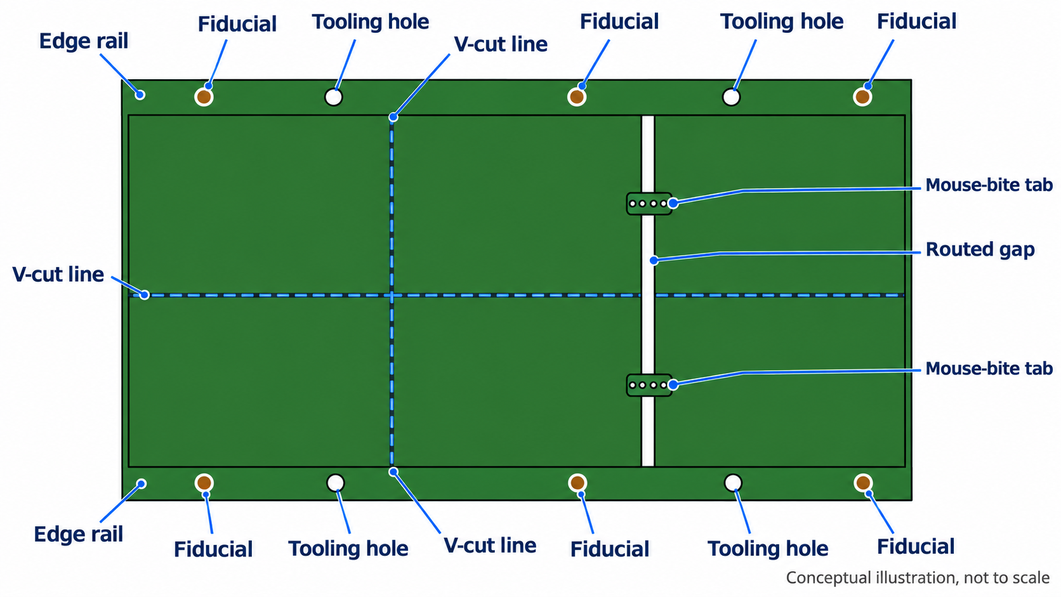
Figure 2: Anatomy of a production panel and its separation lines
Panelization is what makes small boards practical to build. A board a few centimeters across is too small to clamp on an SMT line. Inside a panel, it moves through the PCB assembly process like one large board, so each step from paste printing to reflow runs once for many copies. Depaneling reverses that choice. The weak connections that held the array together are snapped, cut, or burned through, and each board leaves the frame with its final outline.
How Depaneling Affects Board Edges and Component Reliability
Separation shapes the edge in two ways: its finish and its dimensional tolerance. A snapped V-groove leaves a bevel with a band of broken glass fiber, a broken tab leaves a serrated stub, and a laser leaves a narrow, straight cut wall. Each method also holds a different outline tolerance, which matters when the board must drop into an enclosure or slide into a card guide.
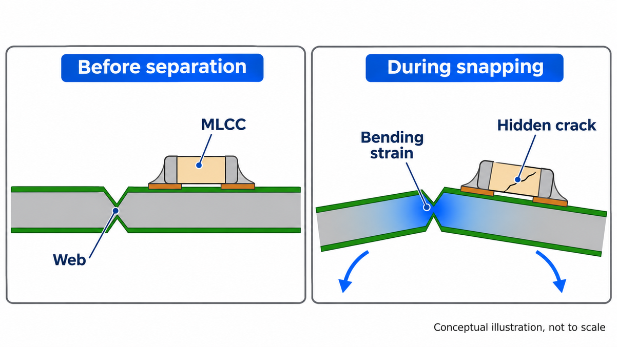
Figure 3: How bending at a separation line strains a nearby ceramic capacitor
The larger risk is to components. Murata's guidance on chip capacitor cracking identifies board breaking and cutting as the steps at which a PCB most easily picks up stress. Snapping a groove bends the laminate around it. A multilayer ceramic capacitor (MLCC) soldered across that zone cannot bend with it, so the ceramic cracks under a terminal. Knowles, a capacitor maker, notes that this stress zone typically extends about 5 mm from a board edge or fixing point. Such a crack is often invisible and can pass the final electrical test.
Comparing the Three Main PCB Depaneling Methods
The three methods differ in what holds the boards together and what separates them. V-cut and mouse-bite are panel connection styles that are broken mechanically, while laser depaneling cuts each board free with a focused beam.
V-Cut Depaneling: Efficient for Straight-Line Separation
V-cut, also called V-scoring, forms a V-shaped groove along the top and bottom of the panel at each board boundary. A common construction, described in JLCPCB's V-cut panelization standards, uses a 25° groove on each side and leaves a web of about one-third of the board thickness. That web keeps the panel stiff enough for assembly, so it survives printing and reflow. Afterward, the boards are snapped apart by hand or run through a rotary-blade depaneler that rolls along the groove.
A scoring blade travels in a straight line across the whole panel. V-cut therefore works only for straight edges, and every line must run from one side of the panel to the other. In return, boards sit edge-to-edge with no gap, which usually makes a V-cut the cheapest option for rectangular arrays. The trade-off is stress: snapping bends the board, so nearby parts see more strain than with the other two methods. The edge is broken rather than machined, so its tolerance is also looser than a routed edge.
Mouse-Bite Depaneling: Flexible for Irregular PCB Shapes
Mouse-bite depaneling, also called stamp-hole panelization, routes most of each board outline and leaves short tabs bridging the gap to the next board or the frame. A row of small drilled holes crosses each tab, perforating it like a postage stamp, so it breaks along the line of holes. A mouse-bite panelization guide from the same fabricator recommends sets of five to eight 0.6 mm holes per tab.
The router can follow any path, so mouse bites suit round, L-shaped, and notched outlines that a scoring blade cannot follow. The tabs are small, and each break is local, which keeps separation stress lower than with V-cut. The costs are a routing gap between boards, which uses more laminate, and a serrated stub where each tab broke. When that stub must go, it is sanded flush, or the tabs are cut with a hook blade or depaneling router instead of being snapped.
Laser Depaneling: Precise, Contactless Separation
Laser depaneling cuts the outline with a focused beam, so no blade, bit, or bending force touches the board. Ultraviolet lasers at 355 nm are the usual choice because nearly all PCB materials absorb UV strongly. They remove material by "cold" ablation, with a smaller heat-affected zone and less debris than a CO2 laser. The CO2 laser's longer wavelength heats the bulk material and focuses to a wider kerf. Because the path is set in software, a UV laser can cut any outline, even on assembled boards.
The limits are speed and cost. A laser removes material in repeated passes, so it typically cuts more slowly than mechanical separation, especially through thick laminate. The equipment also costs far more than a scoring line or router. In practice, the outline and the parts nearest the edge determine which of the three methods is used.
| Method | Outline Shapes | Edge After Separation | Stress on Parts | Best Fit |
|---|---|---|---|---|
| V-cut | Straight lines across the panel | Smooth bevel, light fiber residue | Highest (board is bent) | Rectangular boards at volume |
| Mouse-bite | Any routed outline | Serrated stubs at each tab | Low (local tab break) | Irregular outlines, small to medium runs |
| Laser | Any outline, set in software | Narrow, clean kerf | No mechanical stress | Thin, dense, or flex boards |
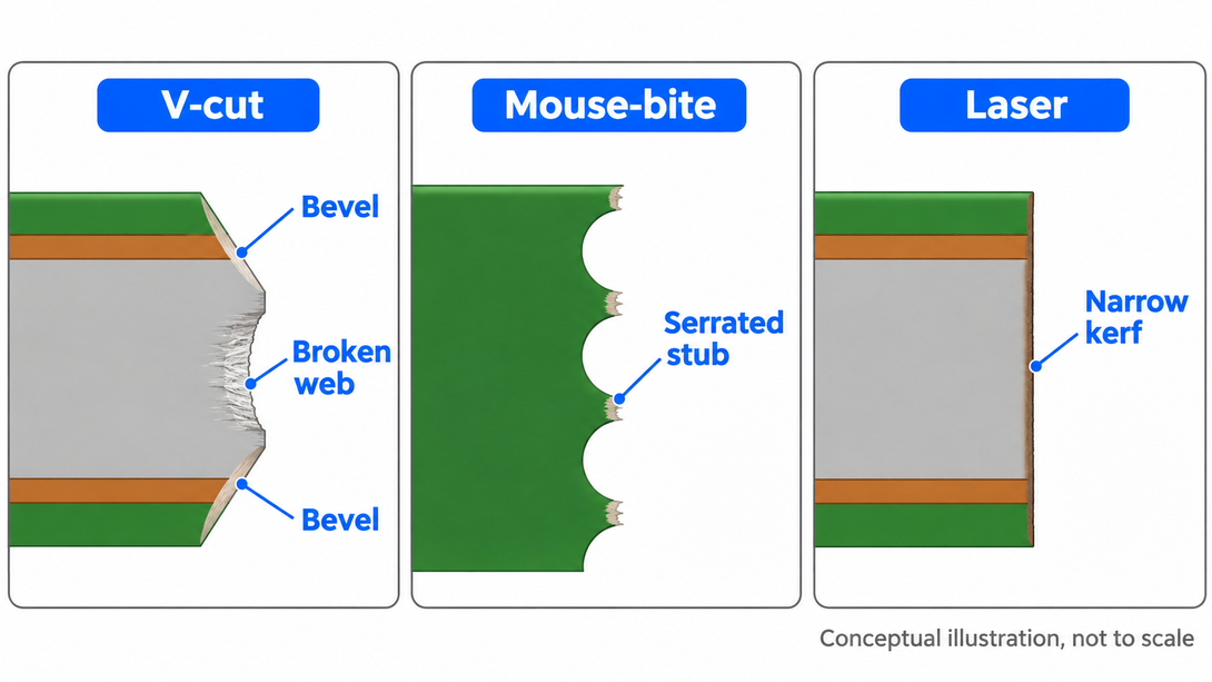
Figure 4: Edge cross-sections left by V-cut, mouse-bite, and laser separation
How to Select the Best Depaneling Method for Your PCB
The method is chosen during layout, not after assembly, because it determines the board spacing, keep-outs, and panel outline. Three questions settle it: what the board geometry allows, what the edge and nearby parts can tolerate, and what the build volume justifies.
Consider PCB Shape, Thickness, and Panel Layout
Outline comes first because it rules out methods. A board with straight edges can be V-cut. An outline with arcs, protrusions, or notches needs mouse bites or a laser, since a scoring line cannot curve and must cross the full panel. Mixed panels are common and practical: V-cut along one axis and mouse bites or routing along the other.
Thickness narrows the choice next. V-cut relies on a web that survives assembly yet snaps cleanly, which needs enough laminate, so it is usually limited to rigid boards of about 0.6 mm and thicker. Very thin rigid boards and flex circuits go to tabs, die cutting, or laser. Panel layout follows from both choices. V-cut boards share their edges with zero spacing, while routed boards need a gap on every side, so the same array takes a larger panel with mouse bites.
Evaluate Mechanical Stress and Edge Quality Requirements
The parts set stress tolerance nearest the separation line, because they take the strain first. A board with MLCCs, BGAs, or connectors within a few millimeters of an edge is prone to mouse bites or laser damage, since neither bends the entire edge. A board with every part set well back can take a V-cut with little risk, keeping the cheaper method available.
Edge quality is the second filter, since some edges are functional surfaces. Boards that slide into rails, mate with a connector housing, or show their edge in a finished product need a smooth, accurate outline. A V-cut gives a straight edge with light fiber residue; mouse bites leave stubs that need sanding; and a laser cut needs no cleanup. Check the method's outline tolerance against the enclosure drawing as part of the same decision.
Balance Production Volume, Precision, and Cost
V-cut is the lowest-cost choice for rectangular boards at volume. The panel needs no routing gap, scoring is fast, and separation needs only a simple blade tool. Mouse bites cost slightly more in routing time and lost laminate, but they handle any outline and suit prototypes and small-to-medium runs. Laser depaneling carries the highest equipment cost and the slowest cut. It pays off when a precise, stress-free edge is a requirement, as on thin multilayer boards, flex circuits, and assemblies with parts at the edge.
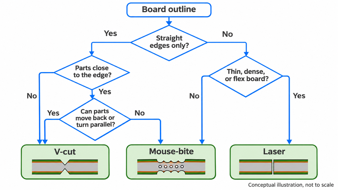
Figure 5: Choosing a depaneling method from board shape, stress, and edge needs
PCB Depaneling Starts with Manufacturing-Ready Panel Design
Clean separation is designed into the panel file, because the groove and tab dimensions, the keep-outs around them, and the rail features must all exist before the fabricator scores or drills anything.
Set Appropriate V-Cut and Mouse-Bite Parameters
Panel parameters come from the fabricator's published capabilities because its scoring and drilling equipment sets the groove angle, hole sizes, and tolerances. The values below come from JLCPCB's PCB capabilities page and show the kind of limits a fabricator publishes.
| Parameter | V-Cut Panel | Mouse-Bite Panel |
|---|---|---|
| Board spacing | 0 mm (boards share the cut line) | 1.6 or 2 mm |
| Copper clearance from the edge | ≥0.4 mm from the V-cut | ≥0.2 mm from routed edges |
| Edge dimension tolerance | ±0.4 mm | ±0.2 mm regular, ±0.1 mm high precision |
| Cut or hole geometry | 25° groove; ≥2 mm between parallel cuts | 0.5-0.8 mm holes; tab ≥5 mm wide |
| Panel and board limits | 70 × 70 mm to 475 × 475 mm; not on 0.4 mm boards | Serrated stubs remain after separation |
Keep Components and Sensitive Areas Away from Separation Lines
Distance sets the first margin: Copper clearance only stops the cut from exposing traces, and components need more room. The same V-cut guidance recommends at least 1.0 mm from the cut centerline to components, and 2.0 mm or more for tall or stress-sensitive parts. Since bending stress typically remains elevated for about 5 mm from an edge, large MLCCs are placed farther back wherever the layout allows.
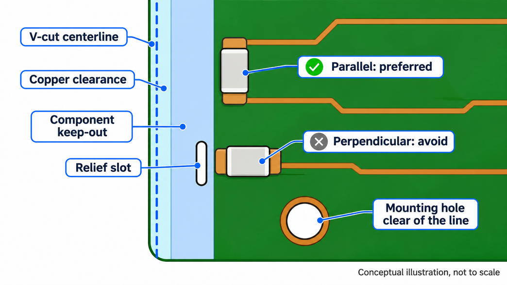
Figure 6: Keep-out zones and part orientation beside a V-cut line
Orientation matters as much as distance: The board bends along the separation line. An MLCC set parallel to that line therefore sees far less strain than one set across it. Murata names parallel orientation as the most effective way to reduce break stress. Where a part cannot be rotated, a routed slot between it and the line isolates it from the bend, and Knowles reports that such a slot can cut the stress on a capacitor by about half.
Holes and tabs need room too: Keep mounting holes away from V-cut lines, since a hole on the line can crack open during separation. Place mouse-bite tabs in blank stretches of the edge, clear of vias, traces, mounting holes, and parts that overhang the outline.
Coordinate Panelization with PCB Assembly Requirements
An assembly line handles the panel, not the board, so the panel must carry what the line needs. Edge rails give the conveyor clamping room, tooling holes locate the panel in the printer, and global fiducials let the placement camera correct for panel offset. For SMT at JLCPCB, the published values are 5 mm rails, 2 mm tooling holes, and 1 mm fiducials. The fiducials are centered 3.85 mm from the panel edge, which keeps them clear of the conveyor guides.
Panel rigidity is the other assembly concern. The connections must survive printing, placement, and reflow. A sagging panel shifts parts, and an early-breaking tab leaves a loose board on the line. Larger panels flex more, which is why assemblers cap panel size well below fabrication limits, and why heavy parts need extra tabs nearby. A design for manufacturing and assembly (DFMA) review before release catches these problems while they are still a file change.
How JLCPCB Supports Reliable PCB Manufacturing
JLCPCB fabricates V-cut, mouse-bite, and hybrid panels and carries the same panel through the assembly process. Its published rules define the spacing, clearance, and rail values a panel needs so that a single panel file can serve both fabrication and assembly.
PCB Fabrication and Panelization for Different Project Needs
There are two routes to a panel. You can upload a single board and select Panel by JLCPCB with edge rails, and the fiducials and tooling holes are then added to the rails, not to each board. Or you can upload your own panel as Gerber files, and it is fabricated as drawn. Two V-cut limits shape the array: at most 25 V-cut lines on either axis, and an extra charge when either side of a piece is 15 mm or less.
Manufacturing Consistency from PCB Production to Assembly
Assembly accepts panels in a form matched to the service. Economic PCBA takes single boards or mouse-bite panels, while Standard PCBA also takes V-cut panels and requires edge rails and fiducials. The recommended maximum for an assembly panel is 250 × 250 mm. Larger panels flex on the conveyor and during reflow, reducing placement accuracy and potentially breaking connection points. Assembled boards ship with the rails attached by default, and a panel removal service can first separate them.
Preparing PCB Files and Specifications for Production
Most panel problems start as file problems, so four checks before upload prevent most of them:
- Mark the separation lines: Label each scored line "V-CUT" and each milled area "CNC" on the same layer as the board outline.
- Add assembly features to a custom panel: In a panel supplied as Gerber files, tooling holes and fiducials are not added for you, so place them on the rails yourself.
- Check clearances against the published rules: Copper, mounting holes, and tabs must meet the separation clearances before the files are released.
- Build tooling from the final engineering files: After order review, download the engineering files and make stencils and fixtures from them, not from your original Gerbers, so they match the panel as fabricated.
FAQs about PCB Depaneling
Q: Is PCB depaneling done before or after assembly?
Usually after. Boards stay in the panel through paste printing, placement, and reflow, because the rails, tooling holes, and fiducials are what the SMT line uses to hold and align them. Bare boards that will be assembled by hand can be separated first.
Q: Is V-cut the same as V-scoring?
Yes. V-cut, V-scoring, and V-grooving all name the same process. A V-shaped groove is cut into both faces of the panel along a straight line, leaving a thin laminate web that is snapped or cut after assembly.
Q: Can you depanel PCBs by hand?
Yes, for V-cut and mouse-bite panels, but hand breaking bends the board unevenly and puts the most stress on nearby parts. A rotary-blade depaneler for V-cuts, or a cutter for tabs, separates the boards with more controlled stress.
Q: Can flex PCBs be V-cut?
No. V-cut needs a rigid laminate thick enough to leave a breakable web, and a flex circuit is too thin and pliable to snap. Flex circuits are typically separated by laser cutting or by punching with a die, and UV lasers cut polyimide film with a small heat-affected zone.
Q: What is tab routing?
Tab routing cuts most of each board outline with a CNC router and leaves short breakaway tabs, often perforated with mouse-bite holes, to hold the boards in the panel. It suits any outline, and the edge is cleaner when the tabs are cut rather than snapped.
Conclusion
Choose the depaneling method during panel layout because it fixes the spacing, keep-outs, and finished edge. Use V-cut for rectangular boards with parts set back from the edge. Use mouse bites for irregular outlines or stress-sensitive parts near the edge, and laser for thin, dense, or flexible boards that cannot take any bending. Then design the panel according to the fabricator's published rules and connect the ceramic capacitors in parallel along the separation line. When your panel is ready, upload it to JLCPCB and get an instant quote.
Keep Learning
PCB Depaneling for Cleaner Edges and Reliable Production
Key Takeaways Timing: Depaneling happens post-soldering, putting stress directly on finished parts. Methods: Choose V-cut for straight high-volume boards, mouse-bites for irregular shapes, and lasers for stress-free precision. MLCC Safety: Keep parts $\ge$ 1.0 mm from V-cuts, align MLCCs parallel to break lines, or add relief slots. Panel Limits: Cap assembly panels at 250 × 250 mm with 5 mm rails, 2 mm tooling holes, and 1 mm fiducials. File Prep: Mark "V-CUT"/"CNC" on the outline layer, keep copper ......
Step-by-Step Guide to the Printed Circuit Board Manufacturing Process
Key Takeaways Core Role: PCBs provide the physical foundation and electrical connections for modern electronics. Multi-Step Process: Manufacturing spans design imaging, substrate creation, inner/outer layer etching, lamination, and surface finishing. Precision and Quality Control: Features micro-drilling (down to 100 μm) for layer connectivity, Automated Optical Inspection (AOI), and final electrical testing. Protection and Finish: Solder masks and surface finishes (e.g., ENIG, HASL) protect copper tr......
How to Achieve Reliable Through-Hole Soldering on PCBs
key Takeaways Wetting & Fill: Heat the lead, barrel, and planes past melting point with active flux to achieve ≥75% vertical fill. Process & Prep: Bake damp boards to prevent blowholes, and match wave, selective, or hand soldering to board volume. Defect Prevention: Use thermal reliefs to stop heat-sink cold joints, and limit dwell time to avoid pad lifting. DFM & Materials: Size holes to max lead dimensions, keep full annular rings, and choose high-Tg FR-4 for multi-pass durability. Through-hole sold......
Technical Guidance: Character Design Specifications
To facilitate component assembly, future maintenance, and traceability of PCB manufacturing information (such as manufacturer, production date, batch number, etc.), various character markings are typically silk-screened onto the PCB. These include component designators, polarity marks, test point labels, company logos, and production traceability information. Traditional PCB character silk-screening uses the screen printing process, hence the term “silk-screen characters.” High-definition characters a......
Via Filling Explained: Key Techniques, Benefits, and Solutions for High-Performance PCBs
Key Takeaways Via filling completely fills plated through-holes and microvias with epoxy or conductive copper paste, followed by planarization and copper capping (POFV). It eliminates voids, solder wicking, and thermal/mechanical issues while enabling reliable via-in-pad designs. Benefits include superior heat dissipation (up to 8 W/m·K), better signal integrity, higher mechanical strength, and improved assembly yields. JLCPCB provides free non-conductive filling + POFV on 6+ layer boards. Ideal for H......
How Fiducial Markers Guarantee Perfect Alignment in Professional PCB Fabrication
Today, the most sophisticated pick-and-place machine can place a 0.5 mm pitch QFP on its footprint, board after board, thousands of times, and never miss. It is not only a matter of expensive cameras or high-quality servos, but it begins with a little, very small copper dot, simply hanging there in the corner of your PCB. That dot represents a fiducial marker, and without it, even the smoothest SMT line would be laying components in the dark. The unrecognized heroes of automated assembly are the fiduc......