How to Detect PCB Short Circuits by Inspecting Gerber Files
13 min
- What Is a PCB Short Circuit?
- Common Methods for Locating PCB Short Circuits
- Practical Examples: Detecting PCB Short Circuits in Gerber Files
- Important Limitations of Gerber-Based Short Circuit Inspection
- FAQ about PCB Short Circuit Detection
- Conclusion on PCB Short Circuit Detection
Key Takeaways
- PCB short circuits can originate from design issues, manufacturing defects, soldering defects, or component failures; design-related shorts can be spotted before fabrication by inspecting Gerber files.
- Load copper layers, drill files, and solder mask layers in a Gerber viewer like JLCDFM, then look for plated holes that connect copper features belonging to different nets across layers.
- Three practical examples show how to trace shorts: a 12V-to-GND via short, a 3.3V-to-GND short across a two-layer board, and a 5V-to-GND short caused by incorrect copper pour clearance.
- Gerber files describe geometry but not net connectivity, so suspicious connections must be verified with the original design file, DRC, netlist comparison, or electrical testing.
A PCB short circuit can cause anything from unexpected current consumption to component damage or complete circuit failure. While some shorts occur during soldering or manufacturing, others are already present in the original PCB design files.
One way to identify potential design-related shorts before manufacturing is to inspect the Gerber files using a Gerber Viewer. By examining copper layers, drill locations, and their relationships, engineers can spot suspicious connections that may otherwise go unnoticed.
In this article, we'll explain the basic methods for locating PCB short circuits and walk through three practical examples of identifying potential shorts through Gerber file inspection.
What Is a PCB Short Circuit?
A PCB short circuit occurs when two conductive paths that should remain electrically isolated become unintentionally connected. This creates an unintended current path, potentially causing excessive current flow, abnormal heating, power supply instability, or component failure.
Short circuits can originate from several sources:
- PCB design issues: Insufficient clearance between copper features, incorrect copper pours, or unintended connections between different electrical networks.
- Manufacturing defects: Residual copper, incorrect drilling, or other fabrication defects that create unintended conductive paths.
- Soldering defects: Solder bridges between adjacent pads or pins.
- Component failures: Internal shorts caused by damaged or defective electronic components.
This article focuses on design-related short circuits that can potentially be identified by inspecting PCB manufacturing files. For a deeper look at how a complete Gerber package is structured, which layers a fabricator expects, and how to check them in a viewer before upload, see the JLCPCB guide to preparing perfect Gerber files for PCB production.
Common Methods for Locating PCB Short Circuits
Before examining Gerber files, it's useful to understand the common approaches to short circuit troubleshooting. The appropriate method depends on whether the problem originates from the PCB layout, manufacturing process, assembly, or components.
Visual Inspection of Solder Joints
For assembled PCBs, solder bridges are one of the first things to check. Closely spaced pins and pads, excessive solder paste, or soldering process issues can cause solder to connect adjacent terminals.
Inspecting the solder joints under a microscope can help identify visible bridges, particularly around fine-pitch components.
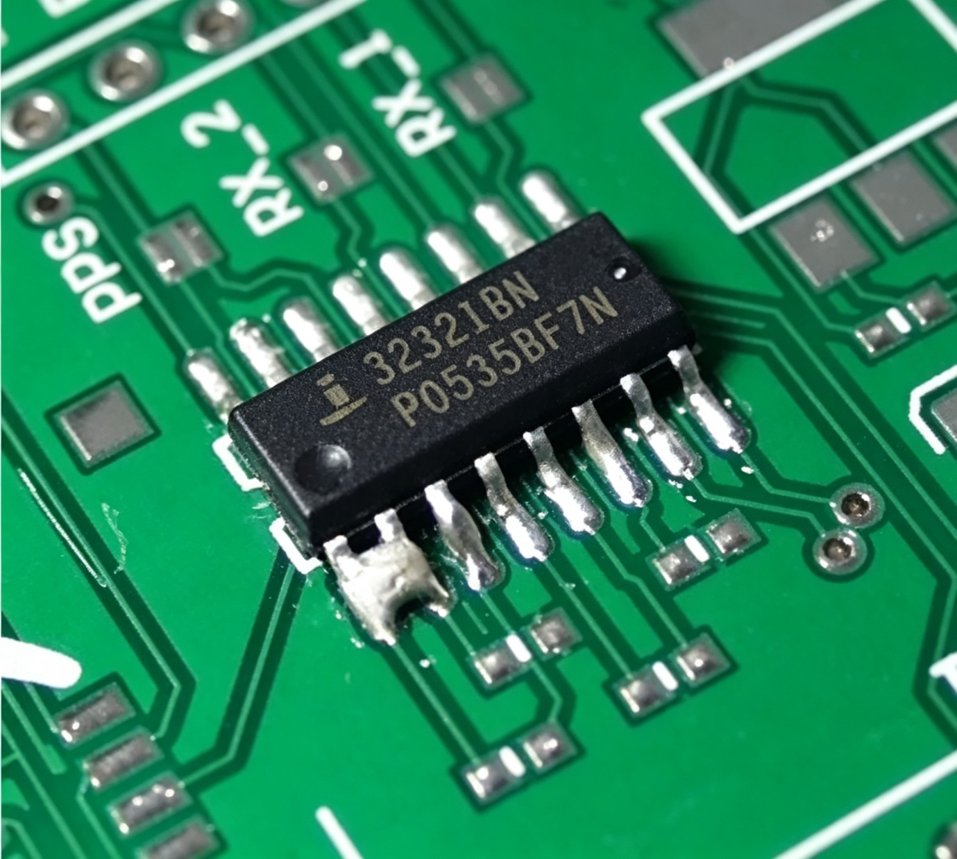
Figure 1: A solder bridge connecting two adjacent fine-pitch pins, one of the most common soldering defects that causes a PCB short circuit.
Thermal Inspection
A short circuit can cause abnormal current flow and localized heating. A thermal camera can help identify unusually hot areas on a powered board.
For safer troubleshooting, use a current-limited power supply and avoid touching an energized PCB directly.
Electrical Short Circuit Testing
A multimeter can be used to measure resistance or check continuity between power rails, such as VCC and GND.
If a short is suspected, a current-limited power supply or a dedicated short-circuit locator can help narrow down the faulty area. However, readings should be interpreted carefully because capacitors and other components may affect resistance measurements.
PCB Design File Inspection
If the short circuit originates from the PCB layout, inspecting the original design file is usually the most direct approach. PCB design software can provide net information and run Design Rule Checks (DRC) to identify clearance violations and unintended connections.
When the original design file is unavailable, Gerber files can still provide useful visual information about copper geometry, drill locations, and potential layer-to-layer connections.
How to Inspect Gerber Files for Potential PCB Short Circuits
Gerber files are commonly used to communicate PCB manufacturing information. They describe the geometric features of individual PCB layers, including copper patterns, solder mask openings, and silkscreen graphics. Drill files provide additional information about hole locations and sizes.
By loading the relevant files into a Gerber Viewer, engineers can examine how copper features are positioned across different layers.
JLCDFM is JLCPCB's free, browser-based Gerber viewer and online DFM checker. Upload a Gerber package (ZIP or RAR, up to 50 MB) to inspect every copper, solder mask, silkscreen, and drill layer, and run an automated DFM and DFA check for clearance and manufacturing issues before the design reaches fabrication.
Open Gerber Files in a Gerber Viewer
First, generate or obtain the complete Gerber package and the corresponding drill files.
Open the files in a Gerber Viewer and make sure the layers are correctly aligned. For short circuit inspection, pay particular attention to:
- Top Copper: Shows copper features on the top layer.
- Bottom Copper: Shows copper features on the bottom layer.
- Inner Copper Layers: Shows internal copper patterns in multilayer PCBs.
- Drill Layers: Shows the locations and sizes of drilled holes.
- Solder Mask Layers: Helps distinguish exposed copper areas and solder mask openings.
For a two-layer PCB, start by displaying the Top Copper, Bottom Copper, and Drill layers together. For multilayer boards, inspect the relevant internal copper layers as well.
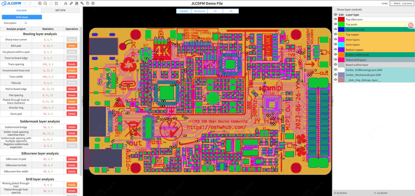
Figure 2: A Gerber file opened in the JLCDFM online viewer. The layer list on the right controls copper, solder mask, silkscreen, and drill layers, while the DFM panel on the left lists clearance and drill-related analysis results for each net.
Understand the Relationship Between Copper Layers and Drill Holes
A key part of Gerber inspection is understanding how holes connect different copper layers.
Not all drilled holes create electrical connections:
- Plated Through-Holes (PTH): The hole walls are plated with copper, allowing electrical connections between the copper layers they pass through, provided the hole intersects the relevant copper pads or annular rings.
- Non-Plated Through-Holes (NPTH): These holes are not copper-plated and do not provide electrical connections between layers.
- Vias: These are plated holes designed to connect copper layers as part of the PCB's electrical routing.
During inspection, look for plated holes that intersect copper features on multiple layers. If those copper features belong to different electrical networks, the connection may create a short circuit.
However, a visual overlap alone does not prove that two different nets are shorted. Gerber files primarily describe physical geometry and generally do not contain complete electrical net connectivity information. The original PCB design or a separate netlist is needed to confirm the electrical relationship.
Practical Examples: Detecting PCB Short Circuits in Gerber Files
The following examples illustrate how copper layers and drill files can be examined to identify potential short circuits.
Case 1: Detecting a Short Between 12V and GND Through a Via
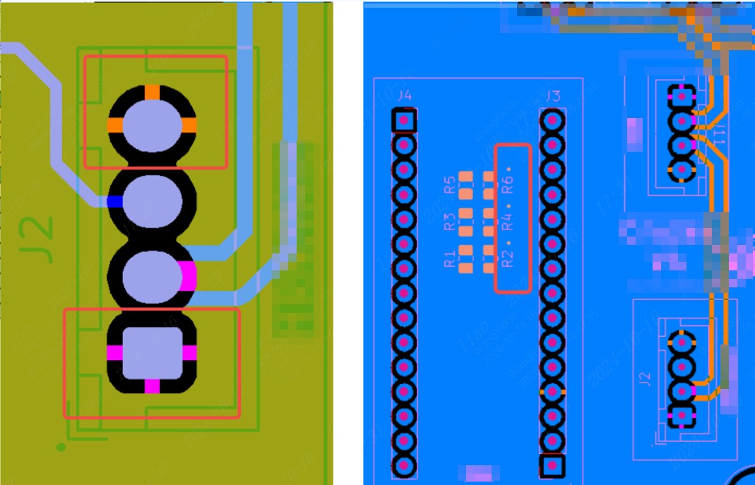
Figure 3: Gerber Viewer screenshot showing the connector J2 and its Pin 1 and Pin 4 locations.
In this case, a PCB was found to have a potential short between the 12V and GND connections at connector J2.
The inspection process was as follows:
Locate the suspicious pins
Open the Gerber files and find connector J2. Identify Pin 1, connected to 12V, and Pin 4, connected to GND.
Trace the copper connections
Inspect the copper layers connected to the two pins. The two pads appear to connect to different copper features on separate layers.
Display the drill layer
Enable the relevant copper layers and the Drill layer. Inspect the plated holes where the copper features intersect.
Check the layer-to-layer connection
The inspection reveals a plated hole connecting the copper features associated with the two pins. Since the two connections belong to different nets, this creates an unintended electrical path between 12V and GND.
This example demonstrates why inspecting only one copper layer may not be sufficient. A potential short can result from the interaction between copper features and plated holes across multiple layers.
Case 2: Detecting a 3.3V-to-GND Short in a Two-Layer PCB
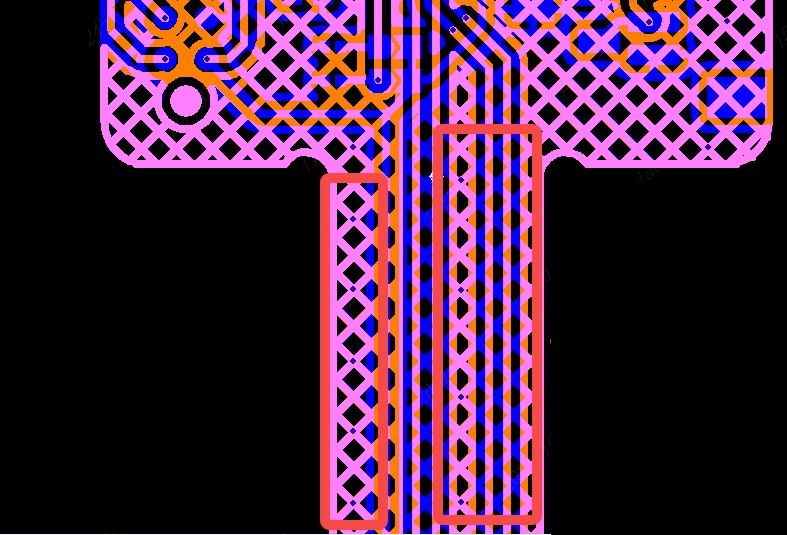
Figure 4: Gerber Viewer screenshot showing the Top Copper, Bottom Copper, and Drill layers of the two-layer PCB.
In this example, a two-layer PCB was reported to have a short between the 3.3V and GND networks across the boards.
To investigate the issue, both copper layers and the Drill layer were displayed in the Gerber Viewer.
The inspection focused on areas where drilled holes overlapped copper features on both the top and bottom layers.
Some holes appeared to connect copper regions on the two sides of the board. If these holes were plated through-holes and the connected copper regions belonged to different nets, they would create an unintended connection between 3.3V and GND.
The important point is to verify both the hole type and the electrical nets involved. A plated hole connecting two copper regions is not necessarily a defect: it is perfectly normal when both regions belong to the same net. The short circuit can only be confirmed when the connected copper features belong to different nets.
Case 3: Detecting a 5V-to-GND Short Caused by Incorrect Copper Clearance
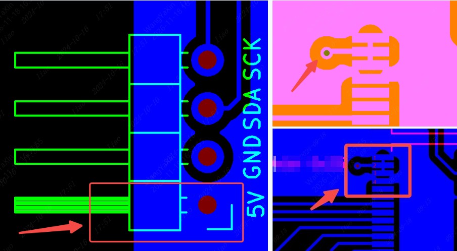
Figure 5: Gerber Viewer screenshot showing the relevant copper pour area and nearby pins.
In this case, a PCB was found to have a potential short between 5V and GND.
The board used two copper layers. During inspection, the relevant power pins and their copper connections were traced across the layers.
The problem was associated with an incorrect copper clearance around adjacent connections.
Locate the 5V and GND connections
Identify the relevant connector pins and determine which copper features are connected to 5V and GND.
Inspect the copper pour
Display the copper layers and examine the clearance around the pads and traces. A copper pour should maintain the required clearance from features belonging to other nets.
Check the suspicious connection area
In the highlighted area, the copper geometry appears to connect adjacent pin regions that should remain electrically isolated.
Follow the connection through the drill layer
Inspect the plated holes and the corresponding copper features on the opposite layer. If the copper connection links the 5V region to a plated hole connected to GND on the other layer, an unintended 5V-to-GND path is formed.
This case highlights the importance of checking copper pour clearances together with layer-to-layer connections. A clearance issue on one layer may become part of a larger short circuit path when vias or plated through-holes connect the copper features across layers.
Important Limitations of Gerber-Based Short Circuit Inspection
Gerber inspection is useful for identifying suspicious copper geometry, but it has important limitations.
Gerber Files Do Not Contain Complete Net Connectivity Information
Standard Gerber files primarily describe the physical shapes and positions of PCB features. They generally do not provide the complete net connectivity information available in the original PCB design.
As a result, two copper regions that appear connected in a Gerber Viewer cannot automatically be classified as a short circuit. They may belong to the same electrical net and be intentionally connected.
Likewise, a drill file alone does not always provide enough information to determine whether a hole is plated. The drill data and the fabrication layer information must be interpreted together.
Verify Potential Shorts with PCB DRC and Electrical Testing
If a suspicious connection is found, use the original PCB design file whenever possible.
The following checks can help confirm the issue:
- Net connectivity inspection: Verify whether the connected copper features belong to different nets.
- Design Rule Check (DRC): Check for copper clearance violations and unintended connections.
- Netlist comparison: Compare the intended electrical connections with the actual PCB layout.
- Electrical testing: Use continuity or resistance measurements to confirm whether the suspected connection exists on the fabricated board.
Gerber inspection should therefore be treated as a way to identify potential short circuits, not as a replacement for complete electrical verification.
FAQ about PCB Short Circuit Detection
Q: Can a PCB short circuit be confirmed from Gerber files alone?
No. Standard Gerber files describe copper, mask, silkscreen, and drill geometry, but they do not carry complete net connectivity information. A viewer such as JLCDFM can highlight suspicious overlaps and tight clearances, but the connection still has to be verified against the original design file, the netlist, or electrical test results.
Q: What is the most common cause of a PCB short circuit?
Solder bridges during assembly are the most common cause, especially on fine-pitch components. Design-related shorts from insufficient copper clearance, copper pour errors, or plated holes that intersect copper belonging to another net form the second major group, and both can be screened before production.
Q: How do I check copper clearance before ordering PCBs?
Run a Design Rule Check in your CAD tool first, then upload the Gerber package to a free DFM tool. JLCDFM checks traces, solder mask, drilling, silkscreen, and component assembly, and reports problems with visual localization before the files reach PCB fabrication.
Q: What is the difference between a via short and a clearance short?
A via short appears when a plated hole connects copper features belonging to different nets on different layers. A clearance short appears when copper on the same layer, such as a pour or a trace, sits closer than the design rule allows and touches another net. The first is a layer-to-layer problem, the second is an in-plane spacing problem.
Q: Can a short circuit be detected after the board is assembled?
Yes. Visual inspection of solder joints, thermal inspection with a camera, and continuity or resistance testing with a multimeter are the standard methods. For assembled boards, the PCBA solder joint inspection guide lists the solder bridge checks to perform on fine-pitch components.
Conclusion on PCB Short Circuit Detection
PCB short circuits can originate from soldering, manufacturing, component failures, or problems in the original PCB layout.
For design-related issues, inspecting Gerber files can help engineers identify suspicious copper connections, insufficient clearances, and potential layer-to-layer shorts. By examining copper layers together with drill files, engineers can better understand how conductive features interact across the board. Once the layout is clean, JLCPCB provides PCB fabrication and SMT assembly, and runs a free DFM check on every order.
However, Gerber files do not provide complete electrical net information. Always verify suspicious connections against the original PCB design, netlist, or electrical test results before concluding that a short circuit exists.
Keep Learning
How to Choose the Right Prepreg Material for Reliable Multilayer PCB
Have you ever wondered what makes all those copper layers stick to a cross-section of a multilayer PCB? Prepreg material is the answer, and it is of much more importance than most engineers think it is. Choose the prepreg selection wrong, and you are predetermined to delamination, impedance drift, and long-term reliability problems. Prepreg is not only glue. It is a designed composite that determines your dielectric separation, dictates your impedance, affects signal loss, and determines your board be......
How to Detect PCB Short Circuits by Inspecting Gerber Files
Key Takeaways PCB short circuits can originate from design issues, manufacturing defects, soldering defects, or component failures; design-related shorts can be spotted before fabrication by inspecting Gerber files. Load copper layers, drill files, and solder mask layers in a Gerber viewer like JLCDFM, then look for plated holes that connect copper features belonging to different nets across layers. Three practical examples show how to trace shorts: a 12V-to-GND via short, a 3.3V-to-GND short across a......
PCB Depaneling for Cleaner Edges and Reliable Production
Key Takeaways Timing: Depaneling happens post-soldering, putting stress directly on finished parts. Methods: Choose V-cut for straight high-volume boards, mouse-bites for irregular shapes, and lasers for stress-free precision. MLCC Safety: Keep parts $\ge$ 1.0 mm from V-cuts, align MLCCs parallel to break lines, or add relief slots. Panel Limits: Cap assembly panels at 250 × 250 mm with 5 mm rails, 2 mm tooling holes, and 1 mm fiducials. File Prep: Mark "V-CUT"/"CNC" on the outline layer, keep copper ......
Step-by-Step Guide to the Printed Circuit Board Manufacturing Process
Key Takeaways Core Role: PCBs provide the physical foundation and electrical connections for modern electronics. Multi-Step Process: Manufacturing spans design imaging, substrate creation, inner/outer layer etching, lamination, and surface finishing. Precision and Quality Control: Features micro-drilling (down to 100 μm) for layer connectivity, Automated Optical Inspection (AOI), and final electrical testing. Protection and Finish: Solder masks and surface finishes (e.g., ENIG, HASL) protect copper tr......
How to Achieve Reliable Through-Hole Soldering on PCBs
key Takeaways Wetting & Fill: Heat the lead, barrel, and planes past melting point with active flux to achieve ≥75% vertical fill. Process & Prep: Bake damp boards to prevent blowholes, and match wave, selective, or hand soldering to board volume. Defect Prevention: Use thermal reliefs to stop heat-sink cold joints, and limit dwell time to avoid pad lifting. DFM & Materials: Size holes to max lead dimensions, keep full annular rings, and choose high-Tg FR-4 for multi-pass durability. Through-hole sold......
Technical Guidance: Character Design Specifications
To facilitate component assembly, future maintenance, and traceability of PCB manufacturing information (such as manufacturer, production date, batch number, etc.), various character markings are typically silk-screened onto the PCB. These include component designators, polarity marks, test point labels, company logos, and production traceability information. Traditional PCB character silk-screening uses the screen printing process, hence the term “silk-screen characters.” High-definition characters a......