Selecting the Right PCB Board Prototype Approach for Rapid Product Testing
18 min
- Decoding PCB Prototyping Essentials
- Exploring Different Methods for PCB Prototyping
- Technical Advantages of Professional Prototype Board Fabrication
- Why JLCPCB is the Leading Choice for PCB Board Prototype Execution
- FAQ about PCB Board Prototype
- Conclusion

Key Takeaways
- Authentic Testing: Prototypes use production-grade materials, stackups, and footprints for realistic design validation.
- Ditch DIY: Breadboards and chemical etching fail on SMD parts, fine traces, and high-speed impedance.
- Early Defect Catch: DFM checks and flying probe tests eliminate short circuits, acid traps, and layout errors before build.
- High-Speed & Thermal: Critical signals need controlled impedance; heat-generating parts require thermal via arrays.
- Fast Delivery: Professional 24-hour rapid turnarounds slash iteration cycles from weeks to days.
Your PCB board prototype is the first time that a schematic must face the real world. The majority of designs do not make it beyond that meeting. That is what you learn in an afternoon or after spending 3 weeks doing nothing useful, depending on the method you choose.
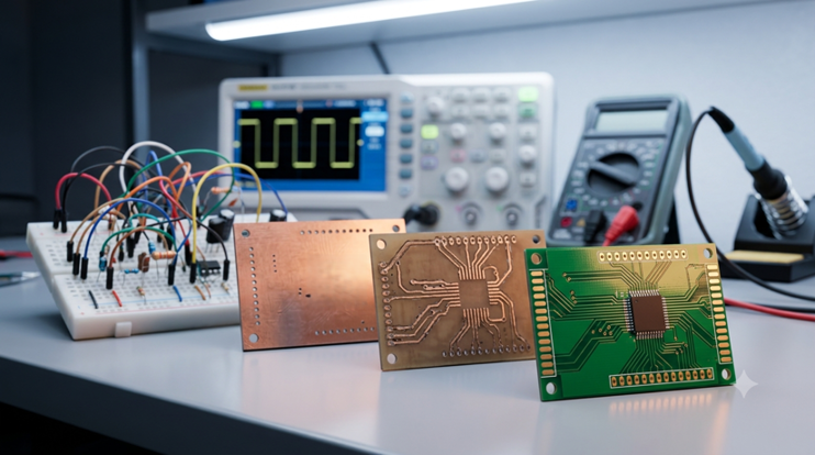
Figure 1: A small batch of freshly fabricated prototype PCBs
In this guide, you will learn:
- What a PCB prototype is and where it fits in hardware validation
- How prototype boards differ from full-scale production runs
- Breadboards, CNC milling, etching kits, and professional fabrication are compared
- Which defects does a DFM review and electrical test catch before you order
- How controlled impedance and thermal design change at the prototype stage
- What fast-turn prototyping costs and how quickly it ships
Decoding PCB Prototyping Essentials
Every hardware project reaches a point where the simulation stops being persuasive. A schematic can be electrically correct and still fail in copper. Solder, laminate, and the enclosure never appear in the netlist, so nothing in your EDA tool models them.
What is a PCB Prototype and Its Role in Hardware Validation
A PCB prototype is a small batch of finished boards, usually 5 to 30 pieces. It is built from the same materials and processes the production run will use. That is what lets you test a design before committing to volume. A prototype is not a rough draft. Same FR-4, same stackup, same footprints, and only the quantity changes. Think of it as the test print pulled off a printing press before the run of ten thousand. The plates, the ink, and the paper are identical to what the run will use. That is exactly what makes the test print worth studying. Change any of them, and you are no longer testing the thing you plan to ship.
A prototype answers three separate questions, and they fail independently. The electrical question is whether the circuit does what the simulation promised. The manufacturing question is whether the board can be built repeatably at all. The mechanical question is whether it fits its enclosure and sheds its heat. Most engineers expect the electrical one to be the problem, so the other two arrive as surprises.
Key Differences Between Prototype Boards and Full-Scale Mass Production
Prototype and production runs come off the same lines with the same capabilities. The real difference is where the money goes. In a five-board prototype, the fixed setup costs dominate, because there is almost nothing to spread them across. In a ten-thousand-board run, those same costs disappear into the unit price. Parts and labor take over as the cost driver instead.
Electrical test works differently in the two volumes. A prototype gets a bare-board E-test or flying probe, which needs no tooling at all. The probes simply move to match the netlist extracted from your Gerber files. Volume production justifies a bed-of-nails in-circuit test fixture instead. That fixture is a machined tooling item costing well over a thousand dollars, so nobody builds one for five boards.
| Factor | Prototype Run | Volume Production | What It Means for You |
|---|---|---|---|
| Typical quantity | 5 to 30 pcs | 1,000 pcs and up | Order spares now; they cost almost nothing |
| Dominant cost | Fixed setup and tooling | Parts and assembly labor | Doubling a prototype quantity barely moves the invoice |
| Electrical test | Flying probe or bare-board E-test | Bed-of-nails ICT fixture | Coverage is thinner, so plan your own bench tests |
| Panelization | Single-up or shared panel | Custom panel, optimized yield | Outline changes are free now and expensive later |
| Lead time | 24 to 72 hours | 2 to 4 weeks with tooling | Schedule iterations in days, not months |
| Design changes | Revise freely between builds | Every change retools the line | Freeze the mechanical outline before you scale |
Exploring Different Methods for PCB Prototyping
Four methods dominate, and they are not competing for the same job. Each one trades manufacturing fidelity against turnaround. So the honest way to choose is to look at what your design actually contains.
DIY Breadboards vs. In-House Desktop CNC Milling
A solderless breadboard is the fastest way to be wrong about a circuit. Each pair of adjacent rows couples through roughly 2 to 3 pF of stray capacitance. A populated board typically carries 8 to 19 pF across the whole circuit. That capacitance sits directly across your signal nodes. So high-impedance nodes drift, and oscillators shift frequency the moment you plug them in.
Inductance is the larger problem, and it comes from geometry rather than materials. Return current is forced back through a distant power rail. The current loop, therefore, encloses a large area, and inductance scales with that area. Measured gain on uncompensated amplifier circuits already droops more than 3 dB at 5 MHz. At 20 MHz, the droop reaches about 12 dB. Treat 10 MHz as the practical ceiling, and you will rarely be caught out. The mechanical limit is just as hard. Nothing surface-mount plugs into a breadboard. An ESP32-S3 module, a QFN regulator, or a 0402 capacitor all need an adapter board. The adapter's own leads then add inductance to the thing you were trying to measure. Breadboards belong to through-hole logic, slow analog, and proof of concept. That is a real job, but a narrow one.
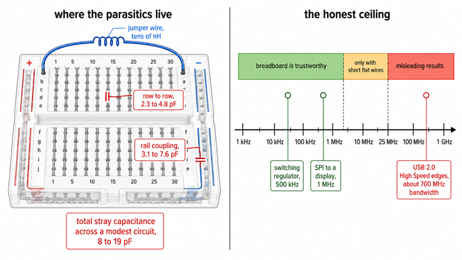
Figure 2: Breadboard parasitics and the frequency ceiling they impose.
Chemical Etching Kits vs. Professional Fabrication Services
Undercut is what limits every etching kit, and it exists because the chemistry is blind to direction. Ferric chloride and cupric chloride dissolve copper isotropically. The etchant eats sideways under the resist edge as fast as it eats downward. A finished trace, therefore, ends up trapezoidal instead of rectangular. The ratio of copper thickness to sideways loss is called the etch factor.
A 1:1 etch factor is what destroys fine features. On 1 oz copper, the trace then loses 35 µm (1.4 mil) from each side. That is 70 µm (2.8 mil) of total width. Meanwhile, the regions that clear last keep etching while you wait for the slow ones. Draw a 0.25 mm (10 mil) trace, and it can arrive at half that width, or open altogether. Home etching is realistic down to roughly 0.25 mm (10 mil) trace and space.
Four gaps stay open no matter how good your technique gets. None of them is fixable with a better tray or a sharper printer:
- Plated through holes, so every two-sided connection becomes a hand-soldered wire, and every through-hole pin needs solder on both faces
- Solder mask, without which 0.5 mm (20 mil) pitch parts bridge during reflow, and nothing stops a stray solder ball from shorting two nets
- Controlled impedance, because impedance is set by a laminated stackup with a known dielectric height, and a single-sided board has no reference plane.
- A protective surface finish, so the bare copper oxidizes and becomes difficult to solder within a few days
Professional fabrication clears all four in a single order, and the capability gap is not marginal. JLCPCB holds 0.09 mm (3.5 mil) trace and space on multilayer boards. Drills go down to 0.15 mm (6 mil), with hole position kept inside ±0.05 mm (2 mil). Copper width tolerance is quoted at ±20%, which sounds loose.
Outsourcing to a Dedicated Prototype PCB Board Manufacturer
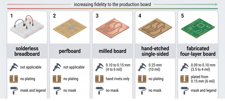
Figure 3: Prototyping method comparison grid across fidelity
Cost is usually where this argument ends. A 2-layer FR-4 board at 100 x 100 mm (3.9 x 3.9 in) starts at $2.00 for 5 pieces. That is less than the laminate and etchant you would consume, making one board badly. Add express shipping, and the outsourced board still costs less than an hour of your own labor.
| Method | Realistic Min Trace/Space | Plated Holes | Layers | Best Use |
|---|---|---|---|---|
| Solderless breadboard | Not applicable | No | 1 | Through-hole logic and analog under 10 MHz |
| Perfboard hand wiring | Not applicable | Manual wires | 1 | One-off through-hole builds you intend to keep |
| Desktop CNC milling | 0.2 mm (8 mil) | No, riveted | 1 to 2 | Same-day RF test coupons and simple boards |
| Chemical etching kit | 0.25 mm (10 mil) | No | 1 to 2 | Single-sided through-hole boards |
| Professional fabrication | 0.09 mm (3.5 mil) | Yes | 1 to 32 | Anything with SMD, multilayer, or impedance control |
What separates a real prototype PCB board manufacturer from a broker is what happens after your upload. A real fab publishes its capability numbers and runs a free design for manufacture review against them. It tells you which rule you broke before it charges you for the board. It also carries an in-house parts library. A prototype that waits three weeks for one regulator has saved you nothing.
Technical Advantages of Professional Prototype Board Fabrication
Three things justify waiting for a courier, and none of them is board quality in the abstract. A professional prototype gets checked before it is built. It is measured while it is built, and tested before it ships. That chain is what turns a board into evidence instead of another variable in your debugging.
Early Defect Detection Through DFM Verification and Electrical Testing
A design for manufacture review reads your Gerbers against the factory's real process limits. It reports what will not survive them. It is not a design review, so it will never tell you the circuit is wrong. But it reliably catches geometry problems that a schematic-level DRC cannot see. Free DFM at JLCPCB runs before the order enters production, so the flag reaches you while a fix still costs nothing.
The recurring flags are dull and expensive. An annular ring under about 0.13 mm (5 mil) can break open when the drill wanders. Drill position is held to ±0.05 mm (2 mil), so the via looks fine on the plot and fails on the board. Acute-angle trace junctions form acid traps, where etchant pools and over-etch the corner. Silkscreen printed across a pad contaminates the solder joint. The PCB silkscreen guide covers the character sizes that stay legible once the ink is clear of copper.
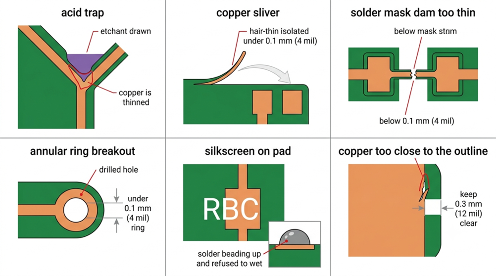
Figure 4: The DFM defect catalog that a pre-production review catches.
Electrical test closes the loop after fabrication. The flying probe test builds a netlist from your Gerber and drill data. Two or more probes are then walked across every net to verify continuity and isolation. No fixture and no minimum quantity are needed. It catches the opens that over-etching creates and the shorts that under-etching leaves. Both hide under the solder mask, where no visual inspection can reach them. JLCPCB electrically tests multilayer boards as standard, and that test costs almost nothing compared to the $60 in parts.
The order in which you power up a new board decides how much a failure teaches you. Work through it in sequence:
- Inspect before soldering anything. Check the silkscreen revision, the board outline, and that the drill pattern matches your connectors.
- Buzz out the power rails for shorts while the board is unpopulated, since a plane-to-plane short found now costs nothing.
- Bring the first board up on a current-limited supply set near 1.5 times the expected idle current, so a mistake browns out instead of burning.
- Measure every rail before any clock runs. A regulator sitting 0.3 V low produces symptoms you will blame on firmware for a week.
- Release the reset line only once the rails are confirmed, then begin functional testing.
Ensuring Trace Integrity, Controlled Impedance, and Thermal Management
Trace integrity starts with accepting that the copper you drew is not the copper you get. Etch tolerance on trace width is ±20%. So a 0.2 mm (8 mil) trace can legitimately arrive anywhere between 0.16 and 0.24 mm (6.3 and 9.4 mil). That is harmless on a logic signal but significant on a power trace, because resistance scales inversely with width.
Controlled impedance becomes a requirement at a specific point, not as a general principle. USB 2.0 High Speed runs at 480 Mbps with edge rates near 500 ps. A signal travels through FR-4 microstrip at roughly 6 ps/mm. So a 500 ps edge is physically about 83 mm (3.3 in) long. The common working rule is that any trace longer than about a sixth of that needs controlled impedance. FR-4 conducts heat at roughly 0.3 W/mK, which is very low. A QFN or a power package cannot conduct heat downward through the laminate beneath it. The standard fix is an array of 0.3-mm (12-mil) thermal vias beneath the pad.
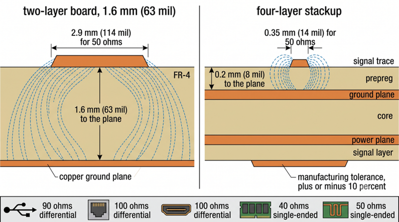
Figure 5: How the stackup sets controlled impedance on a prototype board.
Accelerating Product Time-to-Market with Fast-Turn Prototype Batches
Fabrication lead time, not design effort, usually sets a hardware schedule. Three design spins at a three-week turn is nine weeks of waiting on queues and couriers. The same three spins at a one-week door-to-door turn is three weeks. JLCPCB builds standard FR-4 in 24 hours and metal core in 2 to 3 days. High-frequency laminate takes 4 to 5 days, and flex takes 5 to 6 days, with assembly adding another 24 hours.
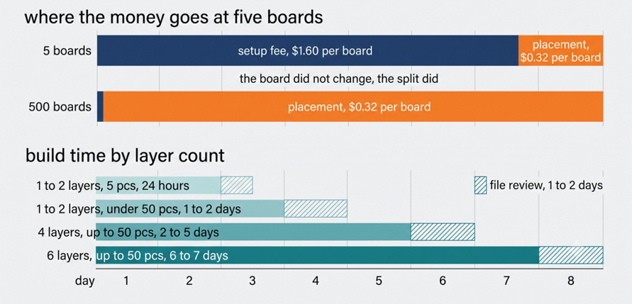
Figure 6: Prototype economics and turnaround, from bare board to assembled batch.
Assembly pricing pushes you in the same direction, because setup cost dominates any small run. Economic PCBA at JLCPCB starts at an $8.18 setup fee plus $1.53 for the laser-cut stencil. It then charges $0.0016 per solder joint. A 200-joint board, therefore, carries 32 cents of joint cost. Running two revisions in parallel beats running them in series. A second $2.00 board is cheaper than a second week of waiting. If two footprint options or two regulator topologies are genuinely undecided, put both in the same order.
Why JLCPCB is the Leading Choice for PCB Board Prototype Execution
A prototype supplier is judged on three things: speed, quoting honesty, and how much checking happens before anything is built. All three matter more at five pieces than at five thousand. One wasted week is a large fraction of a prototype cycle. So the checking is worth more than it looks on a capability page.
High-Speed Production Capabilities and Instant Real-Time Online Quoting
Quoting happens before you commit anything, because the price is computed live from the Gerbers you upload. Change the layer count, the thickness, the surface finish, or the quantity, and the number updates as you click. So you can see what a decision costs while it is still reversible. Upload your files on the JLCPCB quote page, and the DFM report arrives alongside the price.
Parts availability is the other half of the schedule. The in-house library carries over 680,000 in-stock components. Picking from the JLCPCB parts library while you are still drawing the schematic removes the most common prototype delay. That delay is a finished board waiting on one regulator. If the workflow is new to you, the beginner's guide to PCB design covers the footprint side of it. Footprint choice and part availability feed directly into each other.
Industrial-Grade Precision and Automated Quality Inspection at JLCPCB
Multilayer boards hold 0.09 mm (3.5 mil) trace and space. That is what a 0.4 mm (16 mil) pitch BGA escape genuinely needs. Drills go down to 0.15 mm (6 mil), with hole position held inside ±0.05 mm (2 mil). Impedance-controlled stackups are offered from 4 layers through 32, with a ±10% tolerance. So a 90 Ω USB pair or a 100 Ω Ethernet pair can be specified rather than hoped for. Stencils are laser cut to ±0.003 mm (0.12 mil), which keeps 0.4 mm pitch apertures releasing paste cleanly.
| Prototype Requirement | JLCPCB Capability | Why It Matters at Five Boards |
|---|---|---|
| Fine-pitch escape routing | 0.09 mm (3.5 mil) trace and space | A 0.4 mm pitch BGA routes without a redesign |
| Small vias | 0.15 mm (6 mil) drill, ±0.05 mm position | Annular rings survive drill wander instead of breaking |
| High-speed pairs | Impedance control, 4 to 32 layers, ±10% | USB and Ethernet pairs are specified, not guessed |
| Fast iteration | 24-hour FR-4 build, 24-hour assembly | A design spin fits inside one week, door-to-door |
| Catching errors early | Free DFM check plus electrical test | Mistakes are found before parts are soldered on |
Every row exists to remove one specific way a prototype cycle stalls. That is the only useful measure of a fabrication capability at five pieces.
FAQ about PCB Board Prototype
Q: What is a PCB prototype, in simple terms?
A PCB prototype is a small batch of finished circuit boards, typically 5 to 30 pieces. It is built with the same materials and processes as the production run, so it proves the design works electrically, can be manufactured repeatably, and fits its enclosure.
Q: How many prototype boards should I order?
Five is the usual minimum, and it is almost always the right number. Setup costs dominate a small run, so extra pieces add very little. Spares get consumed quickly by destructive testing, by the mechanical team, and by the board you damage during rework.
Q: Is a breadboard good enough instead of a PCB prototype?
A breadboard is fine for through-hole logic and slow analog below roughly 10 MHz. Above that, it's 2 to 3 pF row coupling and large return-current loops make it unreliable. It also cannot accept surface-mount parts, so any QFN, BGA, or 0402 passive needs a real board.
Q: How much does a PCB board prototype cost?
A 2-layer FR-4 board at 100 x 100 mm (3.9 x 3.9 in) starts around $2.00 for 5 pieces before shipping. Assembly is priced separately, starting with an $8.18 setup fee plus $1.53 for the stencil and $0.0016 per solder joint. The setup charge, therefore, dominates small quantities.
Q: How fast can a prototype PCB board manufacturer deliver?
Standard FR-4 builds in about 24 hours, and assembly adds another 24 hours. Metal core takes 2 to 3 days, high-frequency laminate 4 to 5 days, and flex 5 to 6 days. Express shipping typically adds 3 to 7 days, so a full spin fits inside a week.
Q: What does a free DFM check actually catch?
A DFM review compares your Gerbers against the factory's process limits and flags geometry that will not survive fabrication. Typical findings are annular rings under about 0.13 mm (5 mil), acid traps at acute trace angles, silkscreen printed over pads, copper slivers, and copper too close to the routed outline.
Conclusion
Choosing a PCB board prototype method is really a decision about which failures you want to find first. Breadboards and mills find logic errors quickly, but they hide every manufacturing problem. They never run the process that your product will eventually use, so they cannot do otherwise. Professional fabrication finds both kinds at once, and at two dollars for five boards, the cost no longer justifies the argument.
The direction of travel keeps favoring outsourced prototypes as parts shrink. A 0.4 mm (16 mil) pitch BGA, a 90 Ω differential pair, and a plated via array are not bench-buildable at any budget. So the bench methods keep retreating toward the simplest boards. If you want to put these ideas to work, JLCPCB will quote your Gerbers instantly and run a free DFM check against real process limits. A tested batch then ships in about a day.

Popular Articles
• Understanding the Basics of Electronic Devices and Circuits
• Understanding Digital Circuit Timing: Setup Time, Hold Time, Contamination Delay & Clock Skew
• PCBs Explained: A Simple Guide to Printed Circuit Boards
• Guide to the Top 10 Commonly Used Electronic Components
• Digital 101: Fundamental Building Blocks of Digital Logic Design
Keep Learning
A Beginner's Guide to Printed Circuit Board Repair: Common Issues, Methods, and Solutions
Key Takeaways Understand PCB structures, components, and common failure causes to identify repair challenges effectively. Follow a systematic PCB repair process, from fault diagnosis and component replacement to testing and verification. Know when PCB repair is practical and when remanufacturing a new PCB provides a more reliable solution. A printed circuit board (PCB) is a critical part of almost every electronic device. When a board fails, the problem may come from damaged components, broken copper ......
The Hardware Development Process: From Concept to a Finished Electronic Product
Key Takeaways A structured hardware development process turns concepts into functional products through key development stages. Proper PCB design balances performance, manufacturability, and reliability. Early manufacturing considerations help reduce risks and improve prototype success. A reliable PCB partner enables smoother transitions from design to production. Every electronic device you have ever used began as a single idea. A desk lamp that brightens with a tap, a wireless earbud, a controller i......
Demystifying Bare PCB Quality for Reliability-Critical Applications
Key Takeaways Early Defect Catching: Catching faults at the bare board stage costs only the PCB, avoiding wasted components and rework later. Perfboard Risks: Zero PCBs lack reference planes and plated holes, causing signal noise above 10–20 MHz and pad lifting. Critical Material Specs: Reliability depends on hole barrel copper (20–25 µm), Tg, Td, and CTI ratings matching your operating environment. Finish & Shelf Life: HASL and ENIG last ~12 months, while OSP and Immersion Silver/Tin expire in ~6 mon......
A Comprehensive Guide to Capacitor ESR: What It Is, Good Values, and How to Measure It
Key Takeaways Definition: Capacitor ESR (equivalent series resistance) is the single resistance that represents the losses inside a real capacitor, from its electrodes, terminations, electrolyte, and dielectric. Why It Matters: Ripple current flowing through the ESR produces a ripple-voltage step on the supply rail and I²R heating in the capacitor, which limits the capacitor's ripple-current rating and service life. Conditions Matter: ESR varies with frequency, temperature, capacitance, case size, and......
Understanding IPC-6012 Standards for High-Reliability Rigid PCB Fabrication
Key Takeaways IPC-6012 vs. IPC-A-600: IPC-6012 is the binding specification, while IPC-A-600 is only for visual reference. Class 2 vs. Class 3: Class 3 requires thicker copper (25μm vs. 20μm) and zero plating voids. Coupon Verification: Quality is tested by microsectioning panel coupons after thermal stress. Upfront Callout: Specify the class on drawings upfront; boards cannot be upgraded later. IPC-6012 is the line on your fabrication drawing that decides what your supplier is allowed to ship. Most d......
Mastering PCB Plating Types and Process Control in High-Yield Fabrication
Key Takeaways Two-Step Plating: Chemical seed layer comes first, electrolytic copper adds structural strength. Process Choice: Pattern plating enables fine tracks; panel plating suits heavy copper. Via Integrity: Keep aspect ratio ≤ 10:1 to prevent thinnest-point barrel cracking. Surface Finishes: Use ENIG for flat BGA pads and hard gold for high-wear contacts. IPC Standards: Class 2 mandates 20μm copper wall thickness; Class 3 requires 25μm with zero voids. PCB plating turns a stack of drilled lamina......