Medical Device PCB Design: Key Standards and Layout Considerations
20 min
- Introduction
- What Makes Medical Device PCB Design Different?
- Standards That Shape a Medical Device PCB Layout
- Medical Device PCB Stackup and Material Decisions
- Critical Medical Device PCB Layout Rules
- Design for Test, Sterilization, and Long-Term Reliability
- Wireless Medical Devices: Antenna Placement and EMC
- Common Medical PCB Design Mistakes and How to Fix Them
- Medical Device PCB Design Review Checklist
- FAQ about Medical Device PCB Design
- Conclusion: Medical Device PCB Design

Key Takeaways
Constraints come from intended use, not class: Intended use, patient contact, working voltage, and the applicable IEC 60601-1 requirements set the real constraints of a medical device PCB design before routing starts. Device class alone does not.
IPC Class 3 is a choice: IPC Class 3 tightens acceptance, inspection, and documentation, and its tolerances use up design margin. Confirm that the product or procurement spec actually requires it.
Materials must survive the process: Material and finish must survive the cleaning or sterilization method, not only reflow.
Layout decides safety: The isolation barrier, analog guarding, and test access are layout decisions. They get expensive after fabrication.
Evidence is the deliverable: Regulatory frameworks consume design evidence: inputs, records, and verification you can show.
Read the tables, not a rule of thumb: Creepage and clearance come from the tables of the applicable IEC 60601-1 edition. Working voltage, pollution degree, material group, and altitude decide which row applies; no single millimeter value covers every design.
Introduction
Medical device PCB design is the layout of boards for medical electrical equipment so that patient-safety isolation, leakage-current limits, EMC, and traceable design records are built into the board itself. The applicable limits come from IEC 60601-1 and related standards, not from the regulatory class alone.
In medical device PCB design, a board can pass every functional test and still fail a safety check. Picture a patient monitor that exceeds a leakage-current limit because a copper pour was routed too close to the applied-part connector. This is a hypothetical scenario, not a documented incident; the actual root cause would need circuit analysis and testing.
That is why layout is a safety function here, not a cosmetic step. Regulatory classification ranges from Class I to Class III, and similar boards also appear in non-medical consumer products, so no single rule set applies everywhere.
This guide follows the path a layout engineer takes: standards, stackup and materials, layout rules, testability, and a review checklist.
What Makes Medical Device PCB Design Different?
The CAD software, laminates, and design rules are the same ones used for consumer boards. What changes is the cost of being wrong, the evidence trail behind each decision, and the number of people who must approve a change. Two ideas frame the work: how intended use becomes electrical protection, and how regulations become design evidence.
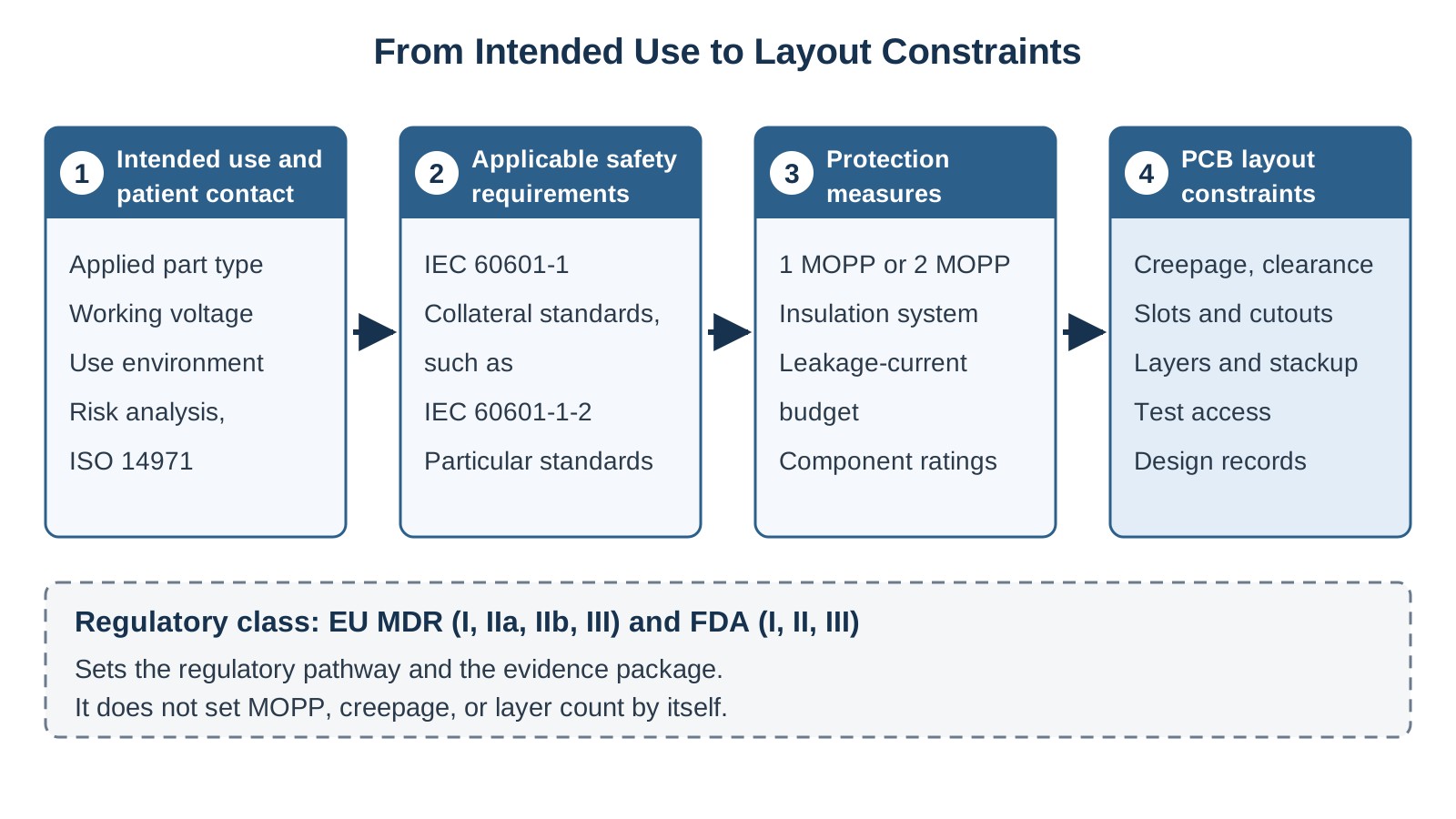
Figure 1. Intended use and patient contact lead to layout constraints. Device class sets the pathway and the evidence, not MOPP or layer count.
Intended Use, Patient Contact, and Risk Classification
EU MDR classes (I, IIa, IIb, III, set by Annex VIII of the regulation) and FDA classes (I, II, III, described on FDA's device marketing page) set the regulatory pathway and the evidence package. See the EU MDR (Regulation (EU) 2017/745) and the FDA guide to studying and marketing your device for the official classification rules. Neither system sets MOPP, creepage, or layer count, and one should not be mapped onto the other. The layout inputs are intended use, the type of patient contact or applied part, working voltage, the ISO 14971:2019 risk analysis, and the applicable IEC 60601-1 requirements.
Compare two cases in medical device electronics design. A consumer wearable with no patient connection has no applied part to protect. Medical electrical equipment with a patient connection does. There, one hazardous situation, leakage current through the patient connection, becomes a creepage requirement, a component choice, and a test point.
How Regulations Become Design Evidence
FDA and EU MDR are frameworks that consume design evidence. They are not PCB rules. FDA pathways (510(k), De Novo, PMA, or exemption) vary by device type and class. EU MDR requires technical documentation and conformity assessment under Regulation (EU) 2017/745. The FDA Quality Management System Regulation (QMSR) took effect on February 2, 2026 and incorporates ISO 13485:2016 by reference. Design History File is a term tied to FDA's earlier design controls, and ISO 13485 speaks of a design and development file, so verify which term your quality system uses.
For the layout, this means a controlled BOM and approved vendor list, revision and change records, a stackup drawing, a DRC report, and verification evidence. Reserve space for UDI marking only where the applicable scheme requires it on the device. The FDA UDI scheme and the EU scheme (Article 27 of the MDR) use different identifiers and timelines. Cybersecurity can add choices such as a secure element or controlled debug access. The UL 2900-2-1 cybersecurity standard for network-connectable healthcare and wellness systems is one device-specific reference, used only where the product calls for it. Confirm the edition your certification body recognizes. A design review signs off on this package.
Standards That Shape a Medical Device PCB Layout
The IEC 60601 guidance below applies to medical electrical equipment within the scope of that series, not to every medical product. An in vitro diagnostic analyzer, for example, is typically assessed against IEC 61010-2-101 rather than IEC 60601-1. Confirm the applicable standards for the specific device before setting PCB design rules.
Standards are written for compliance engineers. Here is the short version: what each one covers, what it changes on the board, and what evidence the layout must produce. Check the edition recognized in your target market before you rely on any row. An IEC publication, its EN adoption in Europe, and the US national adoption, ANSI/AAMI ES60601-1, are not always the same text.
| Standard | What It Changes on the Board | Evidence the Layout Produces |
|---|---|---|
| IEC 60601-1, Edition 3.2 (2020): basic safety and essential performance | Isolation, creepage, clearance, leakage-current budget, applied-part layout | Barrier audit, stackup drawing, leakage budget |
| IEC 60601-1-2, Edition 4.1 (2020): EMC collateral standard | Filtering, ESD protection, return paths, emissions | Protection scheme per port, pre-compliance scans |
| ISO 14971:2019: risk management | Which hazards become layout rules and test points | Risk file linked to each barrier, protection part, and test point |
| ISO 13485:2016: quality management | Design controls and traceability, not spacing rules | Controlled BOM, change records, review records |
| IPC-6012F (rigid boards) and IPC-A-610 (assemblies): performance classes | Tolerances, inspection, and acceptance when a class is specified | Class noted on the fab drawing, DRC rules to match. Confirm the revision cited |
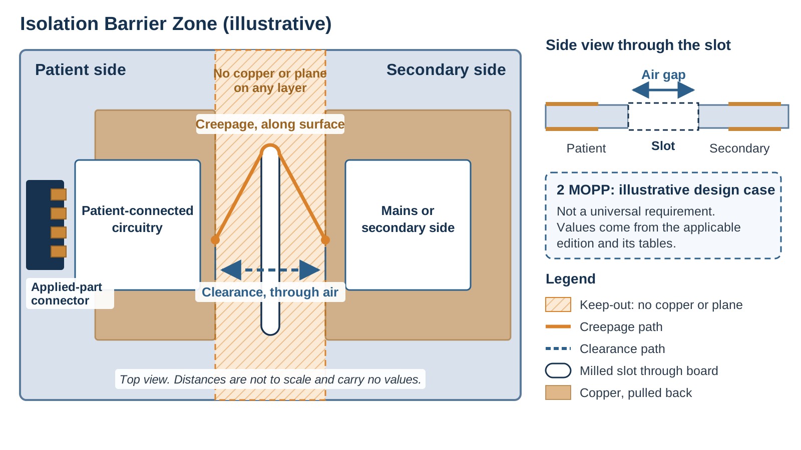
Figure 2. Illustrative isolation barrier with a milled slot. Creepage runs along the surface around the slot end, and clearance runs through air. The 2 MOPP case is an example only.
IEC 60601-1: Isolation, Creepage, and Patient Leakage Current
IEC 60601-1 describes means of patient protection (MOPP): measures that protect the patient from electric shock. 1 MOPP and 2 MOPP differ in the level of protection, and so in the spacing and test voltage that apply. Creepage is the shortest path along an insulating surface. Clearance is the shortest path through air. The two terms are not interchangeable.
The required values depend on working voltage, pollution degree, material group, altitude, and the insulation path involved. Take the final numbers from the tables of the applicable edition. One distance does not fit every design, and 2 MOPP is not a fixed millimeter value.
The layout mechanics are clear, though. Keep copper and planes out of the barrier zone. Mill slots and cutouts where needed. Measure creepage along the surface, including around slots and connector pins. Keep mounting holes and board edges clear of the barrier. Treat solder mask as non-insulating unless the material system and process are qualified for that role.
Leakage current is a budget. PCB surface leakage from flux residue and humidity eats into it, along with every part that bridges the barrier. Y-capacitors, transformers, and digital isolators each add leakage or coupling. A Y-capacitor across the barrier is a conditional choice, set by the isolation architecture, its safety rating, and the leakage budget. It is not a default.
IPC Class 3 and ISO 13485: What Changes on the Layout Side
IPC Class 3 tightens acceptance, inspection, and documentation, and its tolerances use design margin in annular rings, plating, barrel integrity, and conductor spacing. It is not automatically required for medical devices, because IPC leaves the choice of class to the end user, and via-in-pad fill is not a blanket requirement either. The IPC article dates from 2018 and refers to IPC-6012D; confirm which revision your procurement specification calls up, since IPC-6012F (October 2023, superseding IPC-6012E) is the current edition for rigid boards. ISO 13485 is the quality system that makes design controls, change records, and traceability repeatable. It is not a source of spacing rules. For Class 3 fabrication rules, laminate comparison, and finish selection, see the medical PCB manufacturing standards and finishes guide.
Medical Device PCB Stackup and Material Decisions
Decide in this order: the cleaning or sterilization method (if any) and the enclosure first, then the signal chain, then the assembly process. Unit cost comes last. Laminate and surface-finish comparisons live in the manufacturing guide, so this section stays on board type, stackup, and process fit.
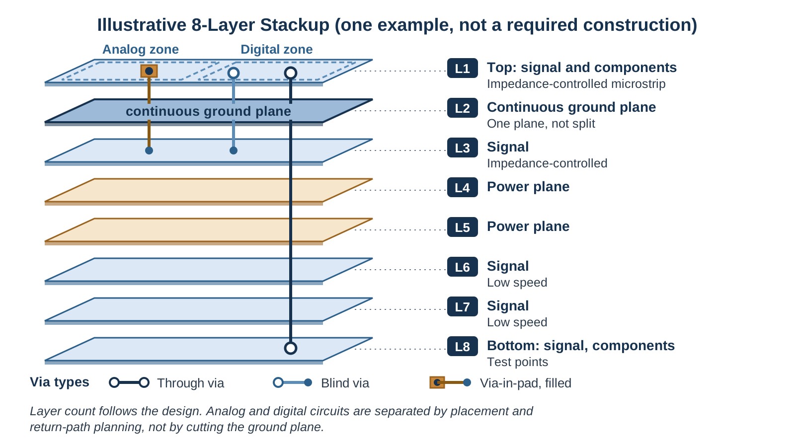
Figure 3. One illustrative 8-layer stackup with a single continuous ground plane. Analog and digital zones are separated by placement, not by a split plane.
Rigid, Flex, or Rigid-Flex: Matching the Board to the Device
Rigid boards suit static, boxed electronics. Flex and rigid-flex earn their cost in moving parts, catheter tips, and body-worn patches. They bring design consequences. Set the bend radius for the layer count and copper type. Add stiffeners under components and connectors. Plan coverlay openings for pads, and anchor connectors so cable pull does not reach the pads. Extra layers in a bend area cost flexibility, so move dense routing to the rigid sections. For fabrication detail, read the medical flex circuits guide.
Medical Device PCB Stackup and Layer Planning
A medical device PCB stackup starts from the signal chain, not from a layer-count habit. Tie the layer count to the isolation barrier, impedance-controlled nets, the RF section, and return-path needs. High-Tg FR-4 is a common starting point for multilayer reflow assemblies. Tg alone does not establish autoclave compatibility, and laminate and finish data are covered in the manufacturing guide linked above.
Two laminate properties act as stackup constraints. Material group, which follows the laminate's CTI, feeds the creepage tables. CAF, conductive anodic filament growth along glass fibers, is a long-term leakage risk, so agree hole-wall spacing and process controls with the fab. Keep Figure 3 honest: one continuous ground plane, with analog and digital separated by placement. Put the stackup drawing, impedance targets, and layer assignment in the design record.
Material Choice Follows the Sterilization Method
Settle this first. Is the device sterilized or disinfected, by which method, and is the board exposed or sealed inside the enclosure? The methods are not interchangeable, and the answer changes the specification: laminate thermal and moisture margin, surface finish (autoclave and chemical exposure, wire bonding, mating cycles), solder mask, via tenting, and coating. The laminate and surface finish comparison sits in the manufacturing guide. A laminate or finish change after validation means a documentation update and often a re-spin.
Critical Medical Device PCB Layout Rules
Four rules explain many field failures and re-spins in medical electronics: the isolation barrier, the guarded analog front end, protection at patient-connected ports, and heat in a sealed housing. Each rule below ends with something you can check.
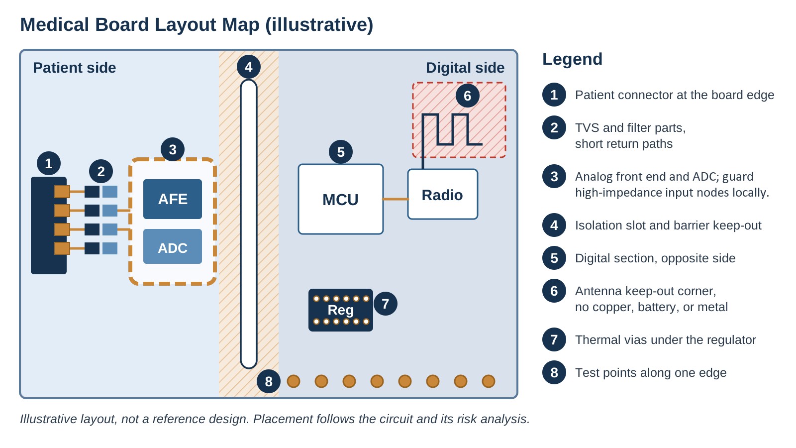
Figure 4. Illustrative layout map: patient connector protection, analog front end and ADC, isolation slot, digital section, antenna keep-out, thermal vias, and test points.
Designing the Isolation Barrier: Creepage, Clearance, and Slots
Place the barrier before routing, not after. Decide where it sits relative to the applied-part connector. The connector pinout is a barrier decision, not a wiring detail, because pin order decides which signals end up near the isolation line. Then apply these rules:
- No copper or plane crosses the barrier on any layer.
- Mill slots under optocouplers, transformers, and digital isolators.
- Measure creepage along the surface, around slots and around connector pins.
- Keep connector pin spacing, mounting holes, and board edges clear of the barrier.
- Count conformal coating toward creepage only when the coating system is qualified for the insulation requirement.
- Avoid sharp copper points, which concentrate electric fields.
A Y-capacitor or another safety-rated part across the barrier is conditional on the isolation architecture, its rating, and the leakage budget. For a barrier audit you can repeat in CAD, set a keep-out rule, put the barrier on its own review layer, measure each distance, and record the result in the stackup drawing.
Low-Level Signal Integrity: Guarding the Analog Front End
ECG, EEG, pH, and photodiode front ends work with very small signals or tiny currents, so leakage paths that would be negligible elsewhere matter here. Surround high-impedance nodes with a guard ring held at a potential close to that of the node and driven from a low-impedance source, and keep other leakage paths away from them. For circuit-specific guard connections and low-impedance drive requirements, see Analog Devices' guidance on layout for precision op amps. Contamination acts as a circuit element. Flux residue, humidity, and gaps in the coating add leakage at high-impedance nodes, so spacing and cleaning are part of the design. Cables and connectors add leakage and pickup at the same nodes.
Grounding depends on the topology. A continuous plane with careful placement is often preferred, and single-point connection is one option for specific mixed-signal topologies, not a rule. Decide from the return paths, the ADC interface, and EMI. Keep a clean analog return path, which is not necessarily a separate analog ground plane, and keep noisy digital return currents away from it. For the general theory, see the ground plane and power plane guide.
EMC and ESD Protection at Patient-Connected Interfaces
IEC 60601-1-2 (Edition 4.1) is the collateral EMC standard. Place TVS or ESD arrays at the connector with short return paths, and filter ahead of the amplifier. Choose protection that does not eat the leakage-current budget, since TVS leakage, TVS capacitance, and filter resistance affect both leakage and signal quality. Where the device must be defibrillation-proof, use protection resistors rated for it. Keep protected traces away from sensitive nodes and off the barrier. More components are not automatically better.
Patient ports do not always need more protection than the digital side. Derive the scheme from the patient-connection type, the risk analysis, the expected electromagnetic environment, and the applicable tests. Apply the same approach separately to each port. For a broader discussion of grounding, return paths, and interference control, see our PCB EMC design guide. One check per port type:
- Patient connection: protection matches the connection type and keeps leakage within budget.
- External communication: protection and isolation follow the risk analysis and the tests.
- Power input: surge and filtering follow the expected environment.
- RF port: filtering and matching suit the radio and the EMC plan.
Thermal Management in Sealed Housings
A sealed enclosure cuts off airflow to the outside, so heat has to leave the board mainly through copper and conduction into the case. Use copper pours, thermal vias, and component derating, and spread heat into the enclosure where the mechanical design allows. Avoid hot spots near patient-contact surfaces, where touch-temperature limits and patient safety apply. For via-array geometry, see the thermal via design guide.
Sterilization or disinfection heat matters only when the device requires that process. In that case the temperature excursion is a second thermal event that stresses joints and laminates. For surface-disinfected devices, do not assume the board must survive steam autoclave cycles.
Design for Test, Sterilization, and Long-Term Reliability
A medical board is typically tested at incoming, in-process, and final stages, so test access is a layout requirement. After release, two things decide long-term results: how the board is tested, and how it survives cleaning and humidity.
Testability: Test Points, Fiducials, and ICT Coverage
Set test point size and pitch with the fixture vendor, keep probes clear of tall parts, and add fiducials for AOI and assembly alignment. Plan bed-of-nails access, and use boundary scan where the parts support it. Treat the programming and debug header as a lifecycle decision. Keep controlled access for development and authorized service, then decide whether it is disabled, removed, or protected before release, based on the security risk assessment. This is not a blanket requirement for every device. In a regulated build, an untested net is an untested risk.
Surviving Sterilization, Disinfection, and Humidity
The method is already fixed in the material choice, so this part covers what the cycle does to the board. Common failure modes are CTE mismatch and delamination, finish oxidation, solder-joint fatigue, coating crazing, and surface leakage under humidity. Useful mitigations are no exposed traces, via tenting, cured conformal coating where specified, a defined gasket or seal interface, and keep-out from the sealing surface. Qualification evidence is cycle-specific, so record the cycle count, temperature, and humidity the design was validated against.
Wireless Medical Devices: Antenna Placement and EMC
In medtech PCB work, connected devices must satisfy both medical EMC and radio requirements, and antenna performance changes once the product is worn or handled.
Antenna Placement and Keep-Out Zones
A body-worn device detunes its antenna, so test with the body or a phantom early. Give the antenna the ground clearance it needs, and keep its keep-out zone free of copper, battery, and metal. Place the matching network close to the feed. A module can simplify RF design, while a chip antenna saves space and cost but needs more tuning. The antenna also interacts with the isolation barrier. Its location, ground reference, and RF return paths must be evaluated together with the isolation architecture. If the radio crosses the barrier, assess the isolation and the RF design together.
Pre-Compliance EMC and Radio Testing
Plan for FCC Part 15 and the EU Radio Equipment Directive alongside IEC 60601-1-2. Run early pre-scans, and add a shield-can footprint with ground stitching. Filter lines that leave the shielded area. Keep test modes and controlled debug access available through certification. Each of these is cheap before fabrication and costly after.
Common Medical PCB Design Mistakes and How to Fix Them
These are generalized patterns from design reviews, not measurements from a single build. This article is a standards-based synthesis, not a test report. Each case follows the same order: mistake, consequence, fix.
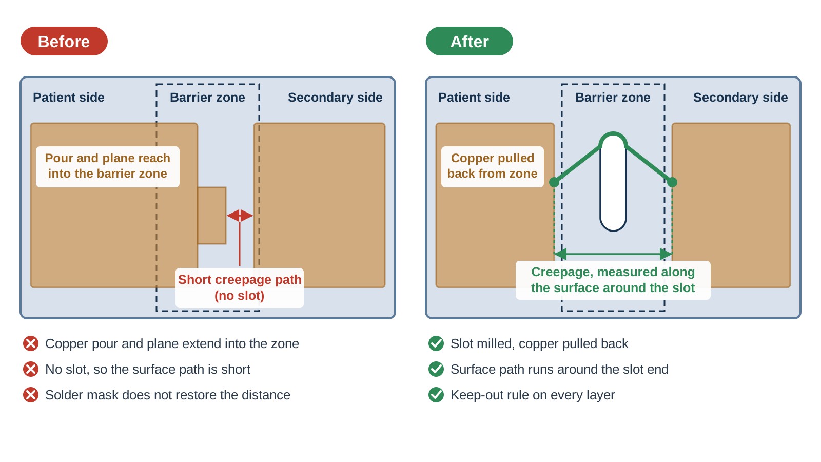
Figure 5. An isolation barrier before and after review: pulling copper back and milling a slot lengthens the surface path.
Undersized or Bridged Isolation Barriers
Mistake: the barrier shrinks during layout edits, or a plane or thermal relief quietly bridges the gap. Consequence: the surface path is shorter than intended, and solder mask does not restore the creepage distance. Fix: add a barrier keep-out to the CAD rules, use a dedicated review layer, and run a dimension check before release.
Split Ground Planes Copied From Audio Designs
Mistake: analog and digital planes are split out of habit. Consequence: return current loses its continuous path, and the split becomes an emissions and crosstalk source near the ADC. Fix: use one continuous ground plane, as in Figure 3, and separate analog from digital by placement. Split only where return-path analysis or the isolation architecture requires it.
Treating Test Access and DFM as an Afterthought
Mistake: test access is requested late. Consequence: vias move, probes crowd together, and margins shrink on fine-pitch parts. Fix: reserve test points and fiducials during placement, run a DFM review before the first prototype, and involve the fabrication and assembly partner at layout freeze.
Medical Device PCB Design Review Checklist
Use this table as a final gate for medical device electronics design. It also covers obsolescence and serviceability, so it checks second sources and footprints, not only the barrier.
| Check Item | What to Verify | Layout Tip |
|---|---|---|
| Intended use and standards | Intended use, patient contact, and applicable standards confirmed | Record them in the design record |
| Isolation barrier | Verified against the applicable MOPP and working-voltage tables | Keep the table reference with the check |
| Creepage and clearance | Checked at connectors, mounting holes, and board edges | Measure on a review layer |
| Barrier crossings | No copper or plane crosses the barrier; slots milled where required | Run a keep-out DRC on every layer |
| IPC class rules | Required IPC class design rules enabled in DRC at project start | Set them before routing |
| Stackup records | Stackup, impedance targets, and layer assignment documented | Attach the drawing to the record |
| Material and finish | Match the cleaning or sterilization method, if any | Confirm before ordering laminate |
| Analog front end | Guarded; return paths and grounding strategy verified | Keep noisy return current away |
| Test and marking | Test points, fiducials, and programming access reserved; UDI or lot marking located per the applicable scheme | Reserve space during placement |
| Second sources | Critical components second-sourced; alternate footprints reserved | Check pads fit both parts |
| Design history | Stackup drawing, DRC report, and review records archived | Archive at every release |
| Port protection | EMC and ESD evaluated separately for patient, communication, power input, and RF ports | Do not copy one scheme to all ports |
FAQ about Medical Device PCB Design
Q: What standards apply to medical device PCB design?
For medical electrical equipment within its scope, IEC 60601-1 addresses basic safety and essential performance, while IEC 60601-1-2 addresses electromagnetic compatibility. Confirm any applicable collateral and particular standards for the specific device. ISO 13485 covers quality management and ISO 14971 covers risk management. IPC Class 3 applies only when the product or procurement specification requires it. FDA and EU MDR are regulatory frameworks, not PCB rules.
Q: Which PCB material is best for medical devices?
There is no single best material. High-Tg FR-4 is a common default, polyimide suits flex and high temperature, and ceramic or PTFE suits RF. The finish follows the sterilization method, cleaning chemicals, and mating cycles.
Q: How much creepage and clearance does a patient-connected circuit need?
It depends on the insulation path, MOPP count, working voltage, pollution degree, material group, and altitude. There is no single figure. Identify the insulation path first, for example mains to applied part, then read creepage from the creepage table and clearance from the clearance table in the edition your target market recognizes. A distance quoted without those conditions is not a requirement.
Q: Do medical device PCBs need special testing?
It depends. Board fabrication inspection, PCBA test, device-level safety and performance testing, and sterilization or environmental validation are separate steps. Select methods from the board structure, assembly process, product risk, and verification plan. Not every test is mandatory.
Conclusion: Medical Device PCB Design
On a medical board, compliance is designed in at the layout stage: isolation geometry, material and finish selection, analog guarding, and test access. Fixing these after fabrication costs a re-spin and a documentation update. Good medical device PCB design starts from intended use and patient contact, turns the applicable standards into checkable layout rules, and keeps the evidence.
To start, upload the schematic and send the isolation, creepage, and clearance requirements as design inputs, and our engineers complete the layout through JLCPCB's layout services. The team works with medical electronics, runs a full DRC during routing, and provides a free review and quotation before payment. Layout does not certify a device, so keep your own compliance process in place.
Keep Learning
Medical Device PCB Design: Key Standards and Layout Considerations
Key Takeaways Constraints come from intended use, not class: Intended use, patient contact, working voltage, and the applicable IEC 60601-1 requirements set the real constraints of a medical device PCB design before routing starts. Device class alone does not. IPC Class 3 is a choice: IPC Class 3 tightens acceptance, inspection, and documentation, and its tolerances use up design margin. Confirm that the product or procurement spec actually requires it. Materials must survive the process: Material and......
Multilayer PCB Design Guidelines: Stack-up and Layout Best Practices
Key Takeaways Stack-up is the foundation: The layer arrangement defines signal integrity, impedance control, and EMI performance — plan it before routing a single trace. Symmetric, reference-heavy designs prevent failures: A balanced stack-up with ground planes adjacent to every signal layer avoids warpage, ensures return path continuity, and minimizes crosstalk. DFM rules ensure manufacturability: Aspect ratio, annular rings, material selection, and symmetric copper distribution are critical to produ......
How to Reduce Noise and EMI in PCB Layout: A Comprehensive Design Guide
Key Takeaways EMI origins: EMI stems from structural layout deficiencies — poor return paths, interrupted reference planes, and large loop areas create antenna structures that radiate unwanted energy. Loop area is critical: Minimizing current loop areas through solid ground planes adjacent to signal layers is the single most effective EMI reduction technique. Placement defines noise: Component placement establishes current loops before routing. Group by function (power, analog, digital, RF), isolate a......
What is the Difference Between PCB Design and Layout?
The difference between PCB design and PCB layout trips up more engineers than you’d expect. While often used interchangeably, these are distinct disciplines. The gap between them is where many projects quietly go sideways. Simply put, PCB design is the logical foundation, while PCB layout is the physical implementation. A flawless schematic can fail in production due to poor layout, and even the best layout engineer can’t rescue it. Below, we provide a detailed breakdown of the differences between the......
How PCB Layout Design Services Improve Circuit Board Performance?
Here is a myth that costs hardware teams money: if the schematic is correct, the board will work correctly. In truth, the schematic will take you halfway. The physical layout is what makes a product really work. PCB layouts transform a circuit diagram into something that you can build and ship. It controls signal integrity, thermal behavior, EMI, and assembly yield simultaneously. With the increased speed and density of designs, it has become a discipline by itself. But not every engineering team can ......
Mastering PCB Design: A Step-by-Step PCB Layout Process Guide
Key Takeaways Process over improvisation: A repeatable, standardized PCB layout process—not luck—is what turns a working schematic into a board that succeeds on the first spin. Placement drives everything: Component layout and functional block partitioning are the most impactful steps; good placement makes routing easy, poor placement makes it impossible. Route critical signals manually first: Clocks, differential pairs, sensitive analog nets, and power switching loops must be hand-routed before auto-......