
How PCB Layout Design Services Improve Circuit Board Performance?
11 min
- Why Good Circuit Board Layout Matters?
- Step-by-Step PCB Design and Layout Process
- PCB Layout Design Rules and Best Practices
- Optimizing PCB Layout for Manufacturing and Reliability
- Frequently Asked Questions
Here is a myth that costs hardware teams money: if the schematic is correct, the board will work correctly. In truth, the schematic will take you halfway. The physical layout is what makes a product really work.
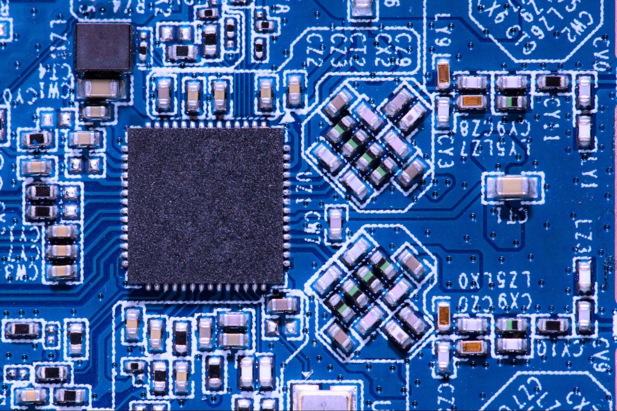
PCB layouts transform a circuit diagram into something that you can build and ship. It controls signal integrity, thermal behavior, EMI, and assembly yield simultaneously. With the increased speed and density of designs, it has become a discipline by itself.
But not every engineering team can get a load of that. As the designs become more complex, they struggle to meet the deadlines and requirements. That’s where PCB layout design services have become a common resource for the engineering teams.
JLCPCB’s exceptional PCB layout services are no different than that. Our years of experience and solid design software are a testament to the quality.
Why Good Circuit Board Layout Matters?
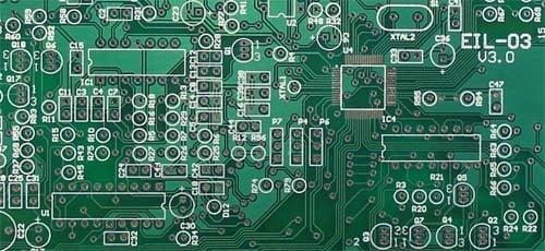
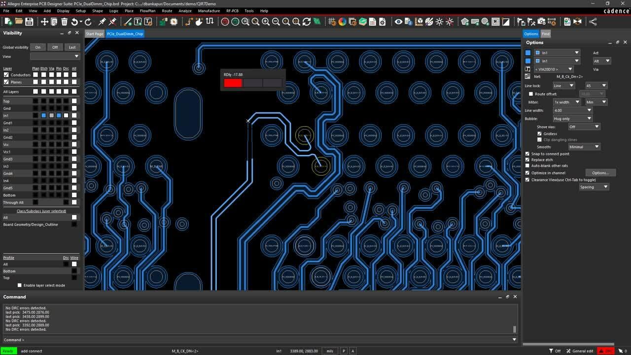
PCB layout refers to the physical implementation of a circuit design, with component placement, trace routing, and layer stackup design. Although the logical relationships are defined by the schematic, the layout determines the physical routes of the signals and power that power overall board functionality.
It is the much-needed linkage between a theoretical design and a high-performance, manufacturable product.
What Poor Layout Actually Looks Like?
Poor design seldom goes horribly wrong. More frequently, it fails at random - boards that work in bench testing, and then fail during initial QA, but then fail during thermal load, or full data rate operation. The decision-making that led to the layout that was causing it was made many months before you had even diagnosed it.
- Signal integrity
One of the victims is signal integrity. Uncontrolled traces that are either too long, too close to each other, or not routed with impedance create crosstalk, reflections, and jitter. These are not visible on a scope at room temperature, with a light load - they are visible when the board is really working hard.
- EMI failures
Layout failures are just about always EMI failures, rather than component failures. The radiating signal trace of a high-speed signal trace is broken in the return path. The board performs well in your bench, doesn’t pass the FCC test, and you are paying to re-test a third time as your launch date gets delayed.
- Thermal failures
Thermal failures are the result of decisions regarding placement that were not made based on thermal analysis. A power device could be alright when in isolation and self-cools when it is in the midst of other sources of heat with no way of dissipating it. The temperature at the junction increases, the component decays, and you end up with field failures that are actually difficult to replicate.
- Assembly defects
This occurs when the geometry of the pad, the orientation of components, or their spacing does not take into consideration the behavioral aspects of the pick-and-place machines and reflow ovens. These are PCB design to manufacture (DFM) failures, and they are reflected in terms of rework costs and yield losses that are directly reflected in the bottom line.
What Does A Good Layout Do?
The proper layout will help to identify such issues before they turn into physical boards. DFM-conscious routing takes into consideration drill tolerances and copper distribution. The board works to its electrical limits, requires less debug time, and does not have any surprises when moving to volume production.
Step-by-Step PCB Design and Layout Process
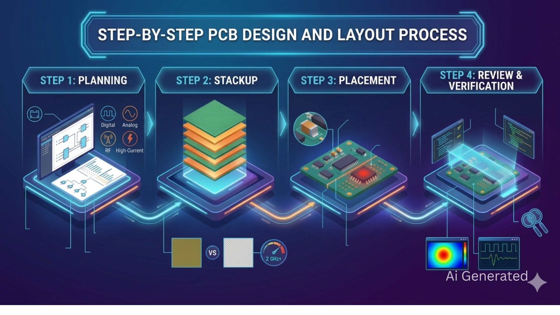
A systematic flow of layout steps can be used to achieve the performance goals of the physical board, without the need to go through costly prototype development. Here’s how the flow looks –
Step 1: Planning and Schematic Design
Layout quality is mostly locked in before the layout tool opens. A clear schematic with structured net lists, marked power domains, and classified signals is important. It provides the layout engineer with the reference context to make good decisions regarding placement. These signals include digital, analog, RF, and high-current. Shortcuts here compound through every phase that follows.
Step 2: Stackup and Material Selection
Stackup planning happens before the first trace is routed. Layer count, layer ordering, dielectric constant, and copper weights all affect impedance control, EMI, and thermal behavior.
FR-4 handles most digital designs well. Above roughly 2 GHz, or when tight impedance tolerance across temperature is required, Rogers or PTFE-based laminates become necessary. No amount of skilled routing compensates for a stackup chosen without considering the electrical environment.
Step 3: Component Placement
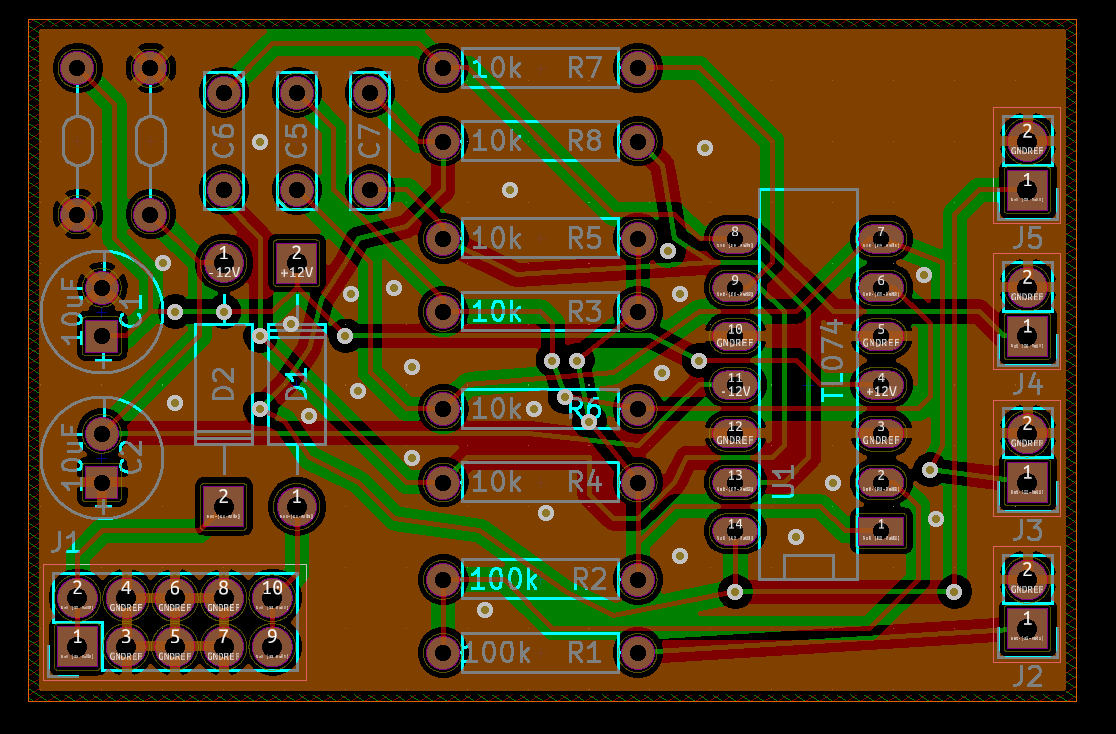
Place first, route second, that's the rule experienced engineers follow without exception. High-power components go near their thermal paths. Decoupling capacitors are as close to IC power pins as the package will allow.
Each additional millimeter of parasitic inductance is undesirable, as it increases the mode of power rail instability during switching. The analog parts must be physically isolated from the high-speed digital logic.
Step 4: Design Review and Verification
Before Gerbers go out, DRC confirms clearances, trace widths, and via specs against manufacturer capability. Netlist comparison catches accidental opens and shorts.
Signal integrity and thermal simulations surface failure modes before they exist in hardware. Professional PCB layout design services add manual engineering review on top of a second set of experienced eyes looking for what software won't flag.
PCB Layout Design Rules and Best Practices
Successful PCB design must be based on a two-fold interest in electrical physics and manufacturing limitations. These basic rules of PCB layout make a working schematic a trusted and high-performance circuit board by focusing on signal integrity and long life.
1. General Layout Rules
General layout guidelines are concerned with disciplined routing and grounding of signals to ensure signal integrity and reduce electromagnetic interference. Some basic PCB board layout rules are –
Calculate trace widths one of current carrying capacity and impedance control to provide stability of signals and avoid reflections.
Use good power and ground planes to offer low-impedance return paths and intrinsic high-frequency decoupling.
Divisions of planes are unnecessary, and discontinuities on the return path are a fundamental source of intractable EMI failure.
Prefer short and direct trace lengths to minimize parasitic inductance and the possibility of electromagnetic crosstalk.
Divide the board into functional blocks - keep power management separate from digital processing - to simplify routing.
2. Layout for Manufacturability (DFM)
DFM principles assure that a design can be produced and assembled without high scrap rates and failure of assemblies at scale. Here's what makes a good PCB design for manufacturing.
Keep ratios of drill to board-thickness below 10:1 to assure dependable copper plating in the vias.
Make sure that the widths of annular rings are large enough to survive the tolerances of drill registration, to avoid breakout open circuits.
Spread copper in all layers evenly to avoid twisting and bending of the board in the course of high-temperature soldering.
The spacing of pads, traces, and edges of the board should obey manufacturer-specific guidelines to avoid shorts during fabrication.
3. High-Current and Sensitive Circuit Layout
Specialized routing techniques are required when dealing with high power levels or sensitive analog signals to prevent thermal overload and noise injection.
Use IPC-2221 standards to size high-current paths based on allowable temperature rise, substituting copper pours for standard traces when necessary.
Follow the "3W Rule" for sensitive signal separation, ensuring the distance between traces is at least three times the trace width.
Connect analog and digital grounds at one point of a star to allow high-speed digital noise to be eliminated before it can corrupt sensitive analog references.
4. Common Mistakes to Avoid
These common design errors can be avoided and save weeks of troubleshooting and costly hardware re-spins.
Do not place a high-speed signal across a gap on a reference plane, which is a huge EMI loop.
Do not put heat-generating components too near each other without sufficient thermal vias or relief.
Skipping final automated checks before tape-out is an expensive shortcut; what a software check catches in minutes can take weeks to fix in physical hardware.
Optimizing PCB Layout for Manufacturing and Reliability

A layout failure is a board that passes prototype test, but fails in volume production, and is not a manufacturing failure. The shift between the functional schematic and a reliable product should be concerned with the way the board will be assembled, maneuvered, and stressed in the actual world.
1. Layout Considerations for Manufacturability
Designing to manufacture (DFM) is a procedure to match the physical layout to the capability of automated production lines to avoid assembly defects.
Placement Clearances: Make sure that there is adequate spacing between components to enable automated pick-and-place nozzles and uniform solder paste application.
Orientation of Components: Unify the orientation of polarized components to ease automated optical inspection (AOI) and minimize the possibility of assembly errors.
Fabrication Limits: Strictly adhere to manufacturer specifications on via diameters, annular rings, and pad sizes to prevent defects on the board level.
Panelization Strategy: Design to be panelized at the layout stage, with edge margins, fiducials, and alignment features added to facilitate high-speed assembly.
2. Reliability in Regard to Layout.
Layout Reliability-oriented design provides the circuit board with a stable operation during the entire lifecycle of the circuit board under different environmental factors.
Thermal Management: Disperse components that generate heat over the board and use thermal vias to transfer heat to internal copper planes.
Mechanical Stress Protection: Locate sensitive components, like oscillators and ceramic capacitors, off-board edges and connectors where mechanical stress and board flexing are greatest.
Power Integrity: Have constant power delivery with low impedance ground planes, wide power traces, and strategically located decoupling capacitors.
Noise Isolation: Isolate route critical signal paths, particularly analog and high-speed clock lines, by isolating them with the switching power supply and other noise sources.
3. When Professional PCB Layout Services are needed
In-house design is not a problem in simple projects, whereas professional PCB layout service is a necessary economic and technical investment with the increase in design complexity.
Expertise Grabs: Expert services are used in cases where the internal engineering department is overburdened or in cases where they do not have the necessary expertise in the latest layout techniques.
Quick Turnaround: It is advisable to outsource layout projects when a project has a time-constrained schedule, and the prototype or produced project is in urgent need.
Technical Complexity: Use a professional assistant when using high-speed, high-density (HDI) or high-layer-count boards, where it is important to control the impedance and return path.
Optimization of Mass Production: Use professional layout engineers to optimize DFM prior to the launch of a product to reduce the scrap rate and reduce the cost per unit.
Operational Flexibility: Use layout services to handle changing design needs without the expense of a full-time employee.
JLCPCB Layout Services will take care of complex multilayer designs to high-speed routing with integrated DFM optimization. We cut the overhead of communication by putting your design in direct contact with the real manufacturing constraints from the very beginning, dramatically reducing your delivery cycles.
Conclusion
A schematic can be correct, and a board can still fail through EMI, thermal problems, assembly defects, or some combination of all three. Layout is where those failures originate, and it's where they have to be solved.
Professional PCB layout design services bring the experience and manufacturing discipline to catch them before they become expensive. For complex designs or production-bound programs, that's not overhead; it's the best risk management available at the design stage.
Frequently Asked Questions
What will I need to deliver to a PCB layout service prior to their starting?
A schematic that is clean and includes footprint references or manufacturer part numbers, mechanical constraints (board outline, connector positions, keep-out areas), and any necessary electrical specifications - target impedances, current limits, frequency ranges.
How does layer count affect cost and performance?
The biggest gain usually comes from going two to four layers of dedicated ground and power planes, cutting EMI and stabilizing power integrity in a way two-layer boards simply can't match. Beyond four, additional layers mainly add routing density and stackup symmetry. Four to six layers is where cost and performance balance out for most commercial electronics.
What does poor signal integrity actually look like?
Unexplained bit errors in high-speed links, clock jitter outside the receiver's tolerance window, elevated analog noise floors, and behavior that shifts when the board moves or when nearby equipment turns on.
Keep Learning
Mastering PCB Design: A Step-by-Step PCB Layout Process Guide
Key Takeaways Process over improvisation: A repeatable, standardized PCB layout process—not luck—is what turns a working schematic into a board that succeeds on the first spin. Placement drives everything: Component layout and functional block partitioning are the most impactful steps; good placement makes routing easy, poor placement makes it impossible. Route critical signals manually first: Clocks, differential pairs, sensitive analog nets, and power switching loops must be hand-routed before auto-......
Multilayer PCB Design Guidelines: Stack-up and Layout Best Practices
Key Takeaways Stack-up is the foundation: The layer arrangement defines signal integrity, impedance control, and EMI performance — plan it before routing a single trace. Symmetric, reference-heavy designs prevent failures: A balanced stack-up with ground planes adjacent to every signal layer avoids warpage, ensures return path continuity, and minimizes crosstalk. DFM rules ensure manufacturability: Aspect ratio, annular rings, material selection, and symmetric copper distribution are critical to produ......
How to Reduce Noise and EMI in PCB Layout: A Comprehensive Design Guide
Key Takeaways EMI origins: EMI stems from structural layout deficiencies — poor return paths, interrupted reference planes, and large loop areas create antenna structures that radiate unwanted energy. Loop area is critical: Minimizing current loop areas through solid ground planes adjacent to signal layers is the single most effective EMI reduction technique. Placement defines noise: Component placement establishes current loops before routing. Group by function (power, analog, digital, RF), isolate a......
What is the Difference Between PCB Design and Layout?
The difference between PCB design and PCB layout trips up more engineers than you’d expect. While often used interchangeably, these are distinct disciplines. The gap between them is where many projects quietly go sideways. Simply put, PCB design is the logical foundation, while PCB layout is the physical implementation. A flawless schematic can fail in production due to poor layout, and even the best layout engineer can’t rescue it. Below, we provide a detailed breakdown of the differences between the......
How PCB Layout Design Services Improve Circuit Board Performance?
Here is a myth that costs hardware teams money: if the schematic is correct, the board will work correctly. In truth, the schematic will take you halfway. The physical layout is what makes a product really work. PCB layouts transform a circuit diagram into something that you can build and ship. It controls signal integrity, thermal behavior, EMI, and assembly yield simultaneously. With the increased speed and density of designs, it has become a discipline by itself. But not every engineering team can ......
PCB Design Rules and Guidelines: A Complete Best Practices Guide
A great schematic is just an idea. To turn it into a real, working product, you need to follow a robust set of Printed Circuit Board Design Rules. Ignoring these rules leads to costly respins, signal integrity (SI) failures, and boards that are physically impossible to build. This guide is a technical resource for the entire design process. We'll cover the essential rules for schematics, layout, and manufacturing that every engineer and hobbyist needs to know for a successful design. What Are PCB Desi......