EMC Design for PCB: EMI, EMS, Testing Standards & Compliance Guide
29 min
- Introduction
- Fundamentals of EMC Design
- PCB Design Techniques for EMI Control
- PCB Design Techniques for EMC Immunity
- EMC Standards and Compliance Requirements
- EMC Testing and Pre-Compliance
- Common PCB EMC Problems and Troubleshooting
- How PCB Manufacturing Affects EMC Performance
- Industry-Specific EMC Design Considerations
- FAQ about EMC Design
- Conclusion
Key Takeaways
- EMC design means controlling both EMI (unwanted emissions) and EMS (immunity to external disturbances); a board that meets emission limits but resets during an ESD test has not achieved EMC.
- Every interference problem can be analyzed with the source–path–victim model, and solved by reducing the source, interrupting the path, or hardening the victim.
- Core PCB techniques include minimizing current-loop area, maintaining continuous reference planes, controlling impedance, decoupling power pins, filtering at interfaces, and protecting external ports.
- EMC must be considered early in design and verified through pre-compliance testing against the applicable IEC/CISPR and regional standards.
- PCB manufacturing choices—stackup, materials, controlled impedance, via structure—directly affect EMC performance and must be reviewed together with the electrical design.
Introduction
A PCB can pass functional testing on the bench yet fail EMC testing or reset when nearby equipment switches. Such problems are often caused by electromagnetic interference rather than firmware faults, and they can be costly when discovered late in development.
EMC should be considered during PCB design, not left until certification. This guide explains EMI emissions and EMS immunity, practical PCB design techniques, EMC testing and standards, common troubleshooting methods, and how PCB manufacturing choices can affect EMC performance.
Fundamentals of EMC Design
What Is EMC Design?
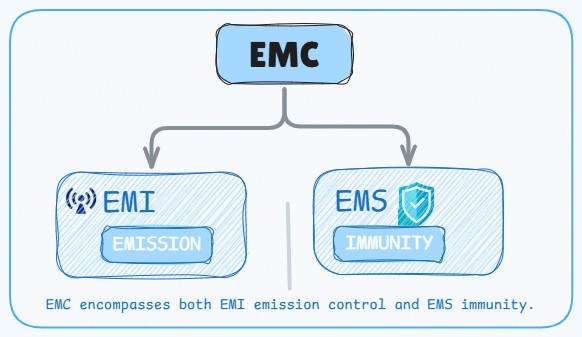
Electromagnetic compatibility is the ability of equipment to function satisfactorily in its electromagnetic environment without introducing intolerable electromagnetic disturbances to other equipment in that environment. In practical terms, a product must both control the electromagnetic energy it emits and tolerate the disturbances it encounters.
These two requirements are commonly discussed as EMI and EMS. EMI (electromagnetic interference) concerns unwanted electromagnetic energy generated or conducted by a device. EMS (electromagnetic susceptibility, often discussed as immunity) concerns the device’s ability to keep operating when exposed to external disturbances. A product that meets emission limits but resets during an electrostatic discharge (ESD) test has not achieved EMC.
EMC design translates these requirements into circuit and PCB decisions. Emission control focuses on limiting noise generation and coupling; immunity design focuses on preventing external disturbances from disrupting sensitive circuits. The methods overlap—for example, sound grounding and filtering can help with both—but the design objective and verification test may differ.
The Source–Path–Victim Model
A useful way to analyze an electromagnetic problem is the source–path–victim model. Every interference problem involves a noise source, a coupling path that transfers the energy, and a victim that is affected by it. A practical solution can therefore target one or more of these elements: reduce noise at the source, interrupt or control the path, or make the victim less susceptible.
Coupling may be conducted or radiated, and it may occur through electric or magnetic fields. Conducted coupling travels along wires, cables, or shared power and ground connections. Radiated coupling transfers energy through electromagnetic fields. Capacitive coupling is associated with electric fields between conductors, while inductive coupling is associated with magnetic fields produced by current loops. These mechanisms can coexist on the same board.
| Element | PCB example | Possible design response |
|---|---|---|
| Source | Switching regulator, clock oscillator, fast digital output | Reduce high di/dt loop area; control switching edges where appropriate; improve local decoupling |
| Coupling path | Shared power or ground impedance, cable, adjacent trace, radiated field | Provide a continuous return path; improve separation; filter at interfaces |
| Victim | Sensitive analog input, reset line, sensor interface | Improve filtering and protection; shorten exposed traces; review grounding and routing |
Conducted and Radiated EMI
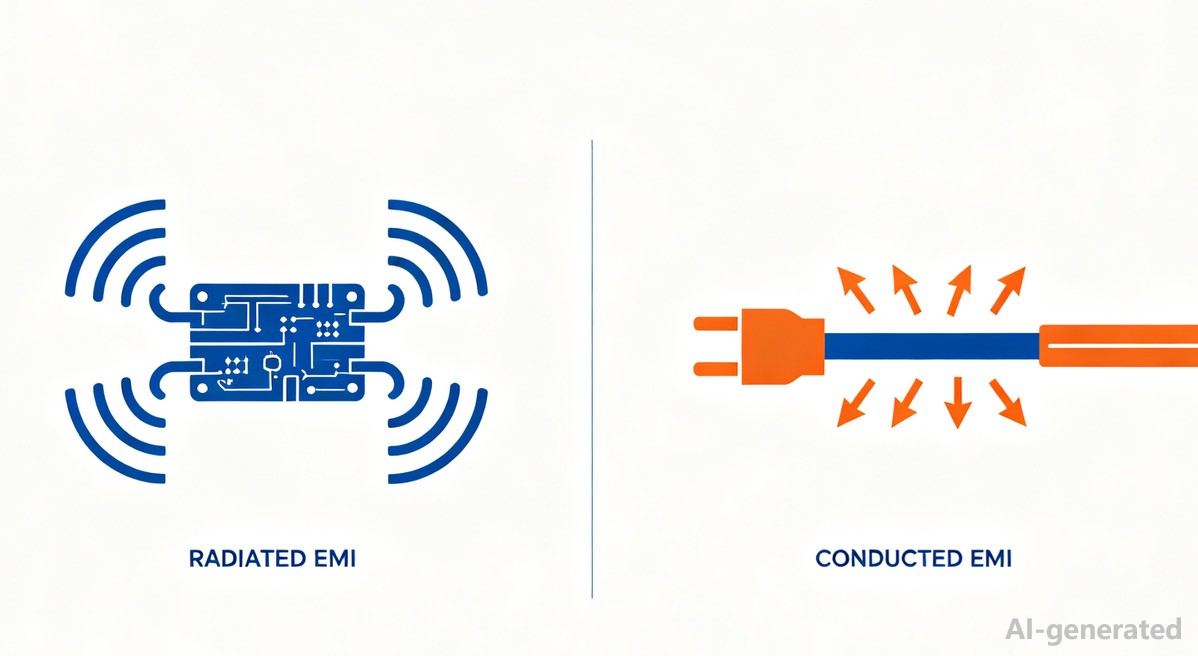
Conducted emissions are unwanted noise voltages or currents that travel along power lines and signal cables. Radiated emissions are electromagnetic fields that propagate through space. Common measurement bands depend on the applicable standard; conducted-emission measurements on AC mains ports often begin around 150 kHz, while radiated-emission measurements commonly begin around 30 MHz. These are typical ranges, not universal boundaries for every product or test.
The distinction is not absolute. Noise conducted onto an external cable can drive common-mode current and make the cable act as an antenna. This is one reason that a board-level problem may appear as a radiated-emissions failure. Common PCB noise sources include clock oscillators and harmonics, switching power supplies, high-speed buses, and poorly terminated signal lines.
Immunity Phenomena Relevant to PCB Design
Immunity testing exposes equipment to disturbances that represent events encountered in its intended environment. Common test phenomena include electrostatic discharge (ESD), electrical fast transient/burst (EFT), surge, radiated radio-frequency (RF) fields, conducted RF disturbances, and voltage dips or interruptions. The applicable tests and severity levels depend on the product family, installation environment, and governing standard.
| Phenomenon | Common reference | What it simulates | Possible product symptom |
|---|---|---|---|
| ESD | IEC 61000-4-2 | Static discharge from a person or object | Reset, latch-up, port damage |
| EFT/Burst | IEC 61000-4-4 | Fast transients associated with switching inductive loads | Communication errors, resets |
| Surge | IEC 61000-4-5 | Higher-energy lightning-related or switching transients | Damaged components, blown protection devices |
| Radiated RF | IEC 61000-4-3 | Exposure to external RF fields | Sensor drift, logic errors |
| Conducted RF | IEC 61000-4-6 | RF disturbances coupled onto cables | Audio noise, data corruption |
| Voltage dips | IEC 61000-4-11 | Short-term supply voltage variations | Brownout or restart |
EMC Measurement Units
EMC measurements use logarithmic units because measured levels can span a wide range. Conducted voltage is commonly expressed in dBµV, radiated electric-field strength in dBµV/m, and power in dBm. In a 50-ohm system, 0 dBm corresponds to approximately 107 dBµV. Peak, average, and quasi-peak detectors respond differently to signal behavior; the detector required for a measurement is specified by the applicable test method.
The margin between a measured result and the applicable limit is important. A design that only just meets a limit may be vulnerable to component variation, cable placement, operating mode, and test uncertainty. The original engineering guidance recommends aiming for meaningful margin, often using 6 dB as a practical design target; this should be treated as a project guideline rather than a universal regulatory requirement.
PCB Design Techniques for EMI Control
PCB Stackup Design for EMC
The PCB layer stackup is one of the most influential decisions affecting electromagnetic behavior. A two-layer board can meet EMC requirements, but it often leaves less freedom for routing and return-current control. A multilayer board can provide dedicated reference planes, making it easier to keep high-speed signal paths close to a continuous reference and reduce loop area.
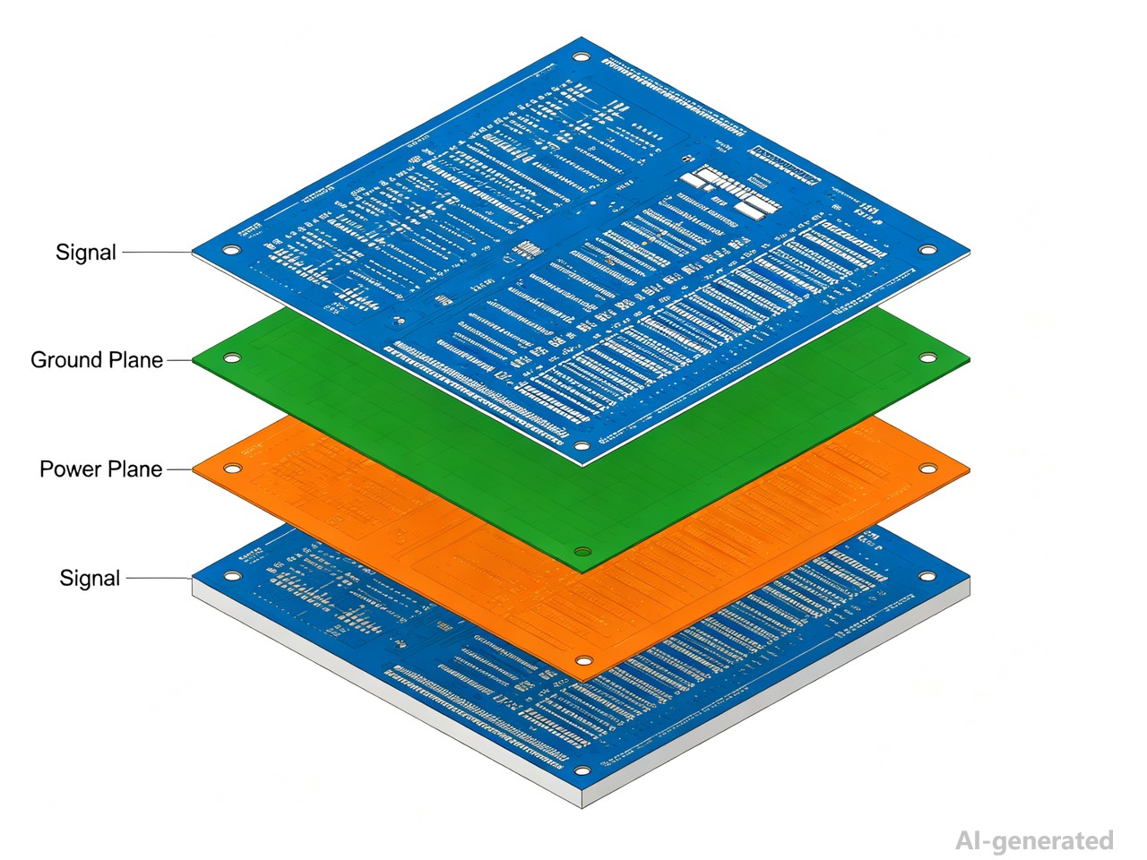
A common four-layer arrangement is Signal / Ground / Power / Signal. It provides a ground reference close to the outer signal layers and a power plane for distribution. Another possible arrangement is Ground / Signal / Signal / Ground, which can provide reference planes adjacent to internal signal layers, depending on the design and fabrication constraints. No single stackup is best for every board; the choice depends on signal speeds, power architecture, component placement, impedance requirements, and manufacturability.
The key principle is that each critical high-speed signal should have a continuous reference path. If a trace crosses a gap or split in its reference plane, its return current may need to detour. The resulting larger current loop can increase inductive coupling and radiated emissions. Stackup planning should therefore consider signal routing and return-current paths together, rather than treating layer assignment as a routing convenience alone.
Component Placement and Circuit Partitioning
Component placement determines where noise is generated and how easily it can couple into other circuits. Place high-noise or fast-switching sections—such as switching regulators, clock sources, and high-speed interfaces—with their current loops and associated components kept compact. Sensitive analog, sensor, and reference circuits should be positioned to reduce exposure to these noisy regions.
Partitioning should reflect the function and current paths of the circuit, not simply create arbitrary physical gaps between analog and digital areas. Keep critical signal paths short, avoid routing sensitive inputs alongside switching nodes or clock traces, and consider where external cables enter the board. Connectors are important boundaries: protection and filtering components should generally be located close to the interface they protect.
Placement, stackup, and routing are interdependent. Moving a switching regulator may shorten its hot loop but lengthen a feedback trace; moving an ESD device may improve access to the connector but complicate its ground return. Review the complete current path and signal reference when making placement decisions.
Grounding and Return-Current Path Design
A PCB ground plane is not an ideal zero-potential point. It has resistance and inductance, and even a short conductor or via can contribute impedance at high frequencies. The objective of grounding for EMC is to provide predictable, low-impedance return paths and avoid forcing high-frequency currents through long or discontinuous routes.
A continuous ground plane is often preferable to unnecessary analog/digital plane splits. A split can interrupt the return path of a signal routed across it, increasing loop area and potentially creating a slot that radiates. Where functional partitioning is needed, it is often better to control component placement and routing while maintaining a continuous reference plane. Separate ground regions may still be appropriate for specific isolation or high-current requirements, but their connection must be deliberately designed.
When a signal changes layers, its return current may also need a nearby path to transfer between reference regions. Ground stitching vias placed near the signal transition can help maintain continuity when the reference arrangement requires it. The original article cites a spacing guideline of approximately one stitching via every λ/20 at the highest frequency of concern; this is a heuristic, not a universal spacing rule. Via placement should be evaluated against the actual geometry, frequency range, and enclosure.
High-Speed Routing and Impedance Control
Minimizing current-loop area is a central routing principle for EMI control. Route high-speed signals over a continuous reference plane, keep the return path close to the signal, and avoid crossing plane splits. Keep clock and other fast-edge nets short where practical, and avoid unnecessary stubs or abrupt routing changes that can create impedance discontinuities.
Controlled impedance helps manage reflections and signal integrity. Common design targets include 50 Ω for many single-ended interfaces and approximately 90–100 Ω for some differential interfaces, but the required value must come from the interface specification and system design. Trace width and spacing depend on the stackup, dielectric properties, copper thickness, and geometry; use a field solver or a manufacturer-supported impedance calculation rather than relying on a generic width rule.
The 3W spacing guideline is sometimes used as an initial rule of thumb to reduce coupling between traces, but it does not guarantee isolation. Actual crosstalk depends on trace geometry, parallel run length, dielectric spacing, reference-plane structure, and edge rate. Differential pairs should be routed with consistent geometry and a continuous reference. Poor symmetry or discontinuities can convert some differential energy into common-mode energy, which may contribute to cable radiation.
Keep high-speed traces away from board edges when practical, and avoid routing them through noisy switching regions. The original article recommends a distance of at least 3H from the board edge, where H is the distance to the reference plane; treat this as a layout guideline to assess for the actual board and enclosure, not as a universal compliance rule.
Power Distribution Network and Decoupling
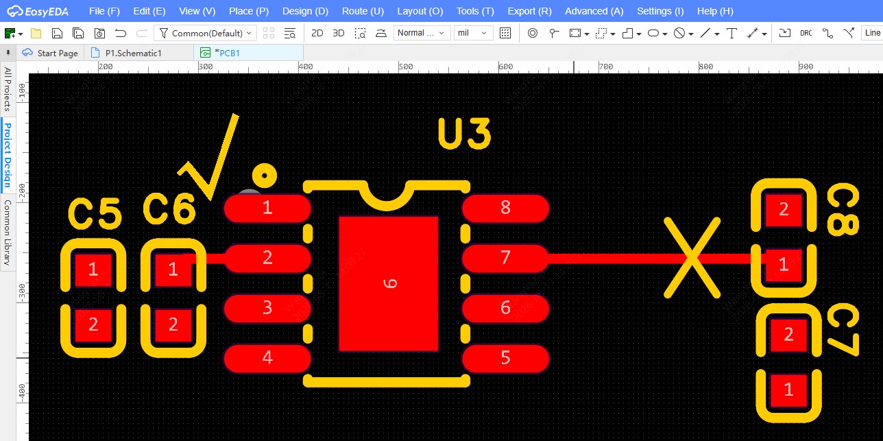
The power distribution network (PDN) should provide low impedance across the frequency range relevant to the circuit. Decoupling capacitors support this goal over different frequency regions: bulk capacitors supply lower-frequency energy demand, while smaller ceramic capacitors are commonly used to address faster current transients near IC power pins. The effective frequency range of a capacitor is limited by its equivalent series inductance and self-resonant behavior.
Placement and connection geometry are as important as nominal capacitance. A capacitor located close to an IC power pin with short, wide connections generally has a lower-inductance path than one placed farther away and connected through long traces or vias. Place the capacitor across the relevant power and ground connections, minimize the loop formed by the IC and capacitor, and follow the component manufacturer’s recommendations for the device and operating conditions.
Multiple capacitors in parallel may be useful when selected and placed as part of a PDN strategy, but adding values indiscriminately can create anti-resonance or fail to address the dominant impedance peak. Validate the PDN approach against the device requirements and, for demanding designs, use impedance analysis or measurement.
Filtering and Shielding at Board Level
Filtering is most effective when applied where unwanted noise enters or leaves a circuit. Power-input filters may combine capacitors, inductors, and common-mode chokes to attenuate differential-mode and common-mode noise. Signal-line filtering may use RC networks or common-mode chokes, provided their electrical characteristics do not compromise the intended signal bandwidth or interface requirements.
Component selection must consider operating voltage, current, insertion loss, parasitic effects, and the impedance environment. For example, a filter that performs well under one source and load impedance may be less effective in another arrangement. Verify the filter in the actual circuit and test configuration.
Shielding cans can reduce coupling into or out of selected PCB regions, but their effectiveness depends on electrical continuity and grounding. A poorly connected shield may provide little benefit and can introduce resonances. A perimeter ground connection with appropriately placed vias is often used to improve the connection between the shield and PCB reference. Shielding should complement good placement, routing, and filtering rather than compensate for avoidable layout problems.
PCB Design Techniques for EMC Immunity
ESD Protection Design
ESD is a common immunity challenge for products with user-accessible connectors, buttons, displays, or exposed conductive parts. IEC 61000-4-2 defines a test method using contact and air discharge. The test levels selected for a product depend on its applicable product or product-family standard and intended environment; do not assume that one level applies to all consumer or industrial equipment.
Transient-voltage-suppression (TVS) devices are widely used to protect interfaces. Select a device with a working voltage compatible with the normal signal level, suitable clamping behavior, adequate surge capability, and sufficiently low capacitance for high-speed interfaces. The protection device should normally be placed close to the connector so that the discharge current can be diverted before it travels into sensitive circuitry.
The protection path matters as much as the TVS device itself. Keep the path from the connector through the protection component to its intended return short and low-inductance. Avoid routing the protected signal in a way that passes the TVS and then runs alongside the unprotected entry path. The appropriate reference may be chassis ground or a PCB reference plane, depending on the product architecture; this decision should be made as part of the system grounding strategy.
EFT and Surge Protection
EFT/burst testing represents fast transient disturbances associated with switching inductive loads and other electrical events. The fast rise time makes parasitic inductance and coupling paths important. Filtering at power and signal interfaces, suitable common-mode suppression, local decoupling, and controlled return paths can help reduce susceptibility.
Surge events generally involve more energy than EFT pulses. The IEC 61000-4-5 combination-wave method uses a 1.2/50 μs open-circuit voltage waveform and an 8/20 μs short-circuit current waveform. Protection architecture depends on the port, expected exposure, and product requirements. In some power-input designs, coordinated stages may include a gas discharge tube (GDT), metal-oxide varistor (MOV), and TVS device. Their ratings, coordination, and layout must be engineered together; simply placing several protection components in series does not guarantee effective protection.
Radiated and Conducted RF Immunity
Radiated RF immunity testing exposes equipment to electromagnetic fields over a specified frequency range and field strength. RF energy can couple through cables, enclosure openings, PCB traces, or unintended structures. Semiconductor junctions may rectify coupled RF energy, creating offsets or disturbances in analog and control circuits.
Design responses include filtering at I/O boundaries, effective decoupling, short and well-referenced sensitive traces, and careful separation between RF sources and susceptible circuits. Common-mode chokes may help on selected cable interfaces, but their suitability depends on the signal type, frequency range, and required data integrity. Test the complete product configuration, including cables and enclosure, because these can dominate coupling behavior.
I/O Interface Protection
External connectors are potential entry points for ESD, EFT, surge, and RF disturbances. Place protection and filtering components close to the relevant interface, and define the current path from the connector to chassis or circuit reference. For low-speed signal ports, TVS arrays may be suitable; high-speed differential ports generally require low-capacitance protection devices that preserve signal integrity. Power ports may need protection selected for their voltage, current, and surge environment.
Avoid routing transient current through sensitive analog or digital ground regions. The best connection depends on whether the product has a conductive chassis, how the connector is mounted, and how the PCB reference is bonded to the enclosure. Document this interface strategy early so that schematic design, PCB layout, and mechanical design remain consistent.
EMC Standards and Compliance Requirements
International EMC Standards
The IEC 61000 series is a foundational family of EMC standards. It defines terminology, test methods, and disturbance phenomena. CISPR (International Special Committee on Radio Interference) publishes emission limits and measurement methods that many regional standards adopt. For automotive applications, ISO 11452 covers radiated immunity for vehicle components, and ISO 7637 covers conducted transients on supply lines. For medical electrical equipment, IEC 60601-1-2 sets EMC requirements.
Regional Regulations and Requirements
Different markets have their own adoption of these base standards. The table below summarizes the major examples listed in the original article; verify the requirements for the specific product category.
| Region | Key Standards | Mark / Requirement |
|---|---|---|
| European Union | EN 55032 (emissions), EN 55035 (immunity) | CE mark under EMC Directive 2014/30/EU |
| United States | FCC Part 15 Subpart B | FCC SDoC (Supplier’s Declaration of Conformity) / certification |
| China | GB 9254, GB/T 17626 series | CCC certification for listed products |
| Japan | VCCI CISPR-based limits | VCCI registration (voluntary in practice) |
| Australia / NZ | AS/NZS CISPR standards | RCM mark |
| South Korea | KN standards | KC certification |
Product-Specific Standards
Generic standards, such as IEC 61000-6-2 for industrial immunity and IEC 61000-6-4 for industrial emissions, apply when no product-specific standard exists. Many product families have dedicated standards: CISPR 32 for multimedia equipment, CISPR 25 for automotive components, IEC 60601-1-2 for medical electrical equipment, and CISPR 15 for lighting. The correct standard should be identified for the product category.
Planning the Compliance Process
A typical EMC project follows this path: design with EMC principles in mind, run pre-compliance tests in-house or at a local lab, fix issues early, and then go to an accredited test house for formal EMC testing. If the product passes, the manufacturer issues a Declaration of Conformity (DoC) or obtains third-party certification, depending on the market. Technical documentation, such as schematics, test reports, and block diagrams, should be maintained as required for the product. Pre-compliance testing helps identify problems before a formal test failure.
EMC Testing and Pre-Compliance
Conducted and Radiated Emission Testing
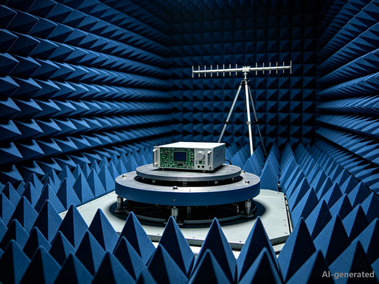
Radiated-emission testing is commonly performed in a semi-anechoic chamber or another facility specified by the applicable test method. The equipment under test is placed in a defined configuration, and antennas measure emissions while the product orientation and antenna position are varied as required. The chamber, ground plane, cable arrangement, operating mode, and measurement distance all influence the result.
Conducted-emission testing on relevant power ports commonly uses a line impedance stabilization network (LISN) to provide a defined impedance and couple disturbance voltage to the measuring receiver. The required frequency range, detector, bandwidth, and limit depend on the applicable standard. Antenna types vary by frequency range; biconical, log-periodic, and horn antennas are examples used in radiated measurements.
Some standards distinguish Class A and Class B limits for different environments or equipment categories. Class B limits are generally more stringent for equipment intended for residential environments, but classification and applicability must be checked against the specific standard. Do not assume that a product can be marketed into a given environment solely from a generic class label.
Immunity Testing and Performance Criteria
Immunity tests apply defined disturbances to the product and assess whether it continues to perform as intended. Performance criteria describe the acceptable behavior during and after the test. A common framework uses criteria such as continued operation, temporary degradation with automatic recovery, or loss of function requiring intervention. The exact criteria and their application are specified by the relevant product or product-family standard; they should not be treated as identical across all EMC tests.
Pre-Compliance Testing
Pre-compliance testing is an early engineering check performed before formal certification. A practical setup may include a spectrum analyzer, near-field probes, a suitable LISN, and equipment for selected immunity checks. Such tools can reveal dominant noise sources and help compare design iterations, although a simplified setup does not replace accredited laboratory testing.
Pre-compliance measurements are most useful when the test configuration is repeatable. Keep cable routing, operating mode, board orientation, probe position, and instrument settings consistent when comparing revisions. The original article recommends targeting around 6 dB of margin as a practical buffer; actual design targets should reflect the applicable limit, measurement uncertainty, production variation, and project risk.
Low-cost, quick-turn PCB prototyping can support iterative EMC development. A revised layout can be fabricated and evaluated before the design is committed to production. The value lies in testing a specific engineering hypothesis—for example, changing a return path or moving a filter—not simply producing multiple revisions without a controlled comparison.
Debugging Tools and Techniques
Near-field probes are useful for locating areas of strong local electric or magnetic fields. H-field probes can help identify current loops and magnetic coupling, while E-field probes can help locate high-voltage or fast-switching nodes. A spectrum analyzer shows frequency-domain behavior; an oscilloscope and suitable current probe can reveal time-domain switching behavior. Thermal imaging may provide supplementary clues about unexpected current concentration, but it does not directly measure EMC.
| Test observation | Potential PCB focus | Useful next check |
|---|---|---|
| Narrow peaks at clock harmonics | Clock routing, return path, cable common-mode current | Probe clock region and cable; compare operating modes |
| Broadband noise from a converter | Switching hot loop, input filter, gate-drive path | Probe switch node and input loop; inspect filter layout |
| ESD causes reset | Connector protection and discharge return path | Check TVS placement and current path to chassis/reference |
| RF exposure shifts analog readings | Sensitive trace coupling, filtering, enclosure/cable path | Compare with filtering or routing changes; inspect external cables |
Common PCB EMC Problems and Troubleshooting
Common EMI Emission Failures
Several recurring patterns account for many emission problems. Clock harmonics may be associated with a fast clock edge, an interrupted reference path, or common-mode current on an attached cable. Switching power supplies can produce conducted noise when the hot loop is large, the input filter is poorly arranged, or switching-node coupling reaches other circuits. High-speed interfaces may radiate when asymmetry or discontinuities convert differential energy into common-mode energy, or when common-mode current drives an external cable.
Common Immunity Failures
ESD-induced resets may result from a protection device placed too far from the connector, a long inductive discharge path, or transient current flowing through a sensitive reference region. EFT can cause communication errors when signal or power interfaces lack suitable filtering and return-path control. Surge events can damage components when the protection network is incorrectly rated or its stages are not coordinated. Radiated RF immunity problems may appear as sensor drift, display glitches, or control errors when sensitive circuits are exposed to coupled RF energy.
A Structured Troubleshooting Workflow
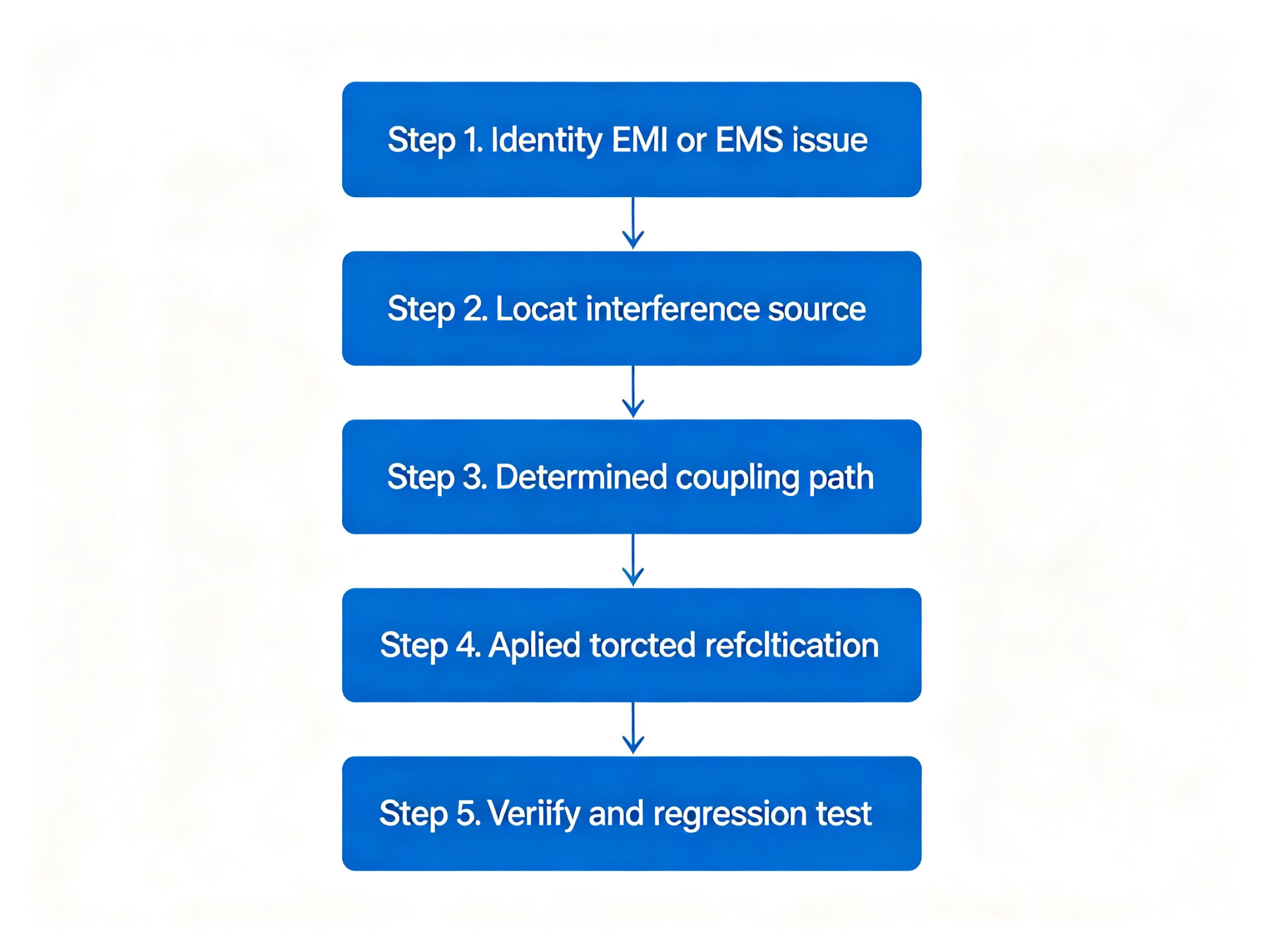
Avoid adding capacitors or ferrites at random. First determine whether the failure is an emission or immunity issue, because the test setup and corrective action may differ. Next, locate the likely source using near-field probing, selective circuit operation, or comparison between operating modes. Then identify the coupling path: power cable, signal trace, current loop, enclosure opening, or external cable. Apply a targeted change at the source or path, and repeat the test using the same configuration to verify the result.
| Observed failure | Likely cause to investigate | Potential corrective action |
|---|---|---|
| Clock harmonic radiation | Clock trace crosses a reference discontinuity; cable carries common-mode current | Restore a continuous return path; review clock routing and interface common-mode behavior |
| Switching supply conducted noise | Large hot loop or ineffective input filtering | Reduce hot-loop area; review input filter placement and connections |
| ESD-induced reset | TVS too far from connector or long return path | Move protection close to entry point; shorten and improve discharge path |
| Differential-interface radiation | Pair asymmetry, discontinuity, or common-mode conversion | Review pair geometry, transitions, termination, and common-mode filtering |
| Analog signal disturbance | RF coupling into a high-impedance or exposed analog node | Review trace exposure, filtering, grounding, and placement |
Why Early EMC Design Matters
The cost and effort of an EMC correction generally increase as a project progresses. A placement or stackup adjustment during design review may be relatively straightforward; a change after fabrication can require a board revision, component changes, and renewed testing. After shipment, an EMC-related field issue can create warranty, service, and reputational costs. Including EMC checkpoints in schematic review, layout review, and prototype testing helps reduce the likelihood of late redesign.
How PCB Manufacturing Affects EMC Performance
PCB Materials and High-Frequency Performance
PCB laminate affects signal propagation through its dielectric properties. The dielectric constant (Dk) is one of the parameters used to calculate characteristic impedance, while the dissipation factor (Df) describes dielectric loss. Material selection should reflect the operating frequency, target impedance, stackup, and electrical requirements. A low-loss material alone cannot correct a discontinuous reference plane or an unnecessarily large current loop.
JLCPCB lists FR-4 laminates from suppliers including Nan Ya, KB, and Shengyi, and also lists two-layer RF PCB options with Rogers and PTFE cores. When selecting a material for a high-frequency design, confirm the specific laminate and dielectric data for the intended construction before completing impedance calculations.
Controlled Impedance and Manufacturing Tolerances
Controlled impedance depends on trace width and spacing, copper thickness, dielectric thickness and properties, and the geometry of the reference plane. The designed stackup and the fabricated board must therefore be considered together. JLCPCB lists controlled-impedance fabrication for 4- to 32-layer boards, with a standard tolerance of ±10%. Its capabilities FAQ also states that ±5% may be available by special request, subject to controlled dielectric materials, stackup design, and additional verification.
Set the target impedance according to the interface specification, then use the manufacturer’s stackup information and impedance calculator to determine suitable trace geometry. Confirm the selected construction before finalizing the routing, since generic trace-width values cannot replace a calculation based on the actual dielectric and copper structure.
Via Structures and PCB Layer Transitions
Via construction affects parasitic inductance, capacitance, and signal transitions. Through vias, blind and buried vias, via-in-pad structures, and backdrilling provide different options for routing density and via-stub management. For high-speed signals, unused via stubs and discontinuities may affect signal integrity; for EMC, layer transitions should also preserve an appropriate return-current path.
JLCPCB lists one-, two-, and three-step HDI fabrication, including laser-drilled blind vias and mechanically drilled buried vias within specified size ranges. Its Via-in-Pad process includes epoxy-filled and capped or copper-paste-filled and capped vias; the published capability page lists this process as the default for boards with six or more layers. JLCPCB also lists backdrilling for 4- to 32-layer FR-4 boards with a thickness of at least 0.8 mm. These processes can support dense routing and selected high-speed interconnect designs, but the via structure alone does not guarantee lower EMI or EMC compliance.
Design for Manufacturing and EMC
EMC requirements and manufacturability should be reviewed together. A selected stackup, dielectric construction, copper weight, impedance target, via structure, and surface finish all need to fit the manufacturer’s available process options. JLCPCB’s published rigid PCB specifications list surface finishes including HASL, ENIG, and OSP, with restrictions for some board types; the appropriate option should be confirmed against the specific design.
JLCPCB provides an online JLCDFM tool with a one-click DFM analysis for uploaded PCB data. This analysis can help identify manufacturability issues before production, while the published PCB capability information provides limits and options for layer count, impedance control, materials, HDI, via-in-pad, and backdrilling. DFM analysis is a manufacturability check, not an EMI/EMS test, and it does not certify EMC performance or guarantee regulatory compliance.
Selected JLCPCB PCB capabilities relevant to EMC-related design decisions (check current specifications before ordering)
| Manufacturing item | JLCPCB published capability | Design relevance |
|---|---|---|
| Layer count and impedance | 1–32 PCB layers; controlled impedance listed for 4–32 layers; standard tolerance ±10% | Supports multilayer stackup planning and impedance-controlled routing |
| Material options | FR-4 laminates from Nan Ya, KB, and Shengyi; 2-layer RF PCB options with Rogers and PTFE cores | Provides listed material options for different electrical and frequency requirements |
| HDI and via-in-pad | 1-step / 2-step / 3-step HDI; blind vias 0.075–0.15 mm; buried vias 0.15–0.55 mm; epoxy-filled & capped or copper-paste-filled & capped Via-in-Pad | Supports denser routing and selected layer-transition / BGA fan-out designs |
| Backdrilling | Listed for 4–32-layer FR-4 boards with thickness ≥0.8 mm | Removes excess via copper from unused layers to reduce via-stub interference |
| DFM analysis | JLCDFM online one-click PCB DFM analysis | Helps identify manufacturability issues; does not verify EMC performance |
Industry-Specific EMC Design Considerations
The EMC environment varies by application, so the design priorities should follow the product’s intended installation and applicable standards. Automotive electronics may face conducted transients, RF exposure, and noise from high-current switching systems. Industrial equipment may be exposed to EFT, surge, variable-frequency drives, and long cable runs. Medical electrical equipment has product-specific EMC requirements that must be considered alongside safety and intended-use conditions.
Consumer and IoT products often combine compact layouts with multiple radio systems and sensitive sensors. Renewable-energy and power-electronics products may involve high-power switching, outdoor wiring, and surge exposure. These application differences affect component selection, interface protection, grounding, filtering, isolation, and test planning.
| Application | Typical EMC challenge | PCB design focus |
|---|---|---|
| Automotive | Conducted transients, RF coexistence, high-current switching | Transient protection, grounding, filtering, isolation and robust layout |
| Industrial | EFT, surge, motor drives and long cables | Interface filtering, surge protection and cable common-mode control |
| Medical | Product-specific immunity and electromagnetic environment requirements | Low-noise layout, isolation where required, and standards-led verification |
| Consumer and IoT | Multiple radios, compact boards and sensitive sensors | RF coexistence, placement, filtering and controlled return paths |
| Renewable energy / power electronics | High-power switching and outdoor surge exposure | Power-stage loop control, isolation, filtering and surge protection |
FAQ about EMC Design
Q: What Is EMC Design in PCB Layout?
EMC design in PCB layout is the practice of controlling electromagnetic emissions and improving a board’s immunity to external disturbances. It involves stackup planning, component placement, grounding, return-current paths, routing, decoupling, filtering, shielding, and interface protection. The goal is to help the complete product operate reliably in its intended electromagnetic environment and meet applicable requirements.
Q: How Do You Design a PCB for EMC?
Start by identifying the product’s applicable EMC requirements and likely noise sources. Plan a stackup that provides continuous reference paths for critical signals, place noisy and sensitive circuits deliberately, minimize high-frequency current-loop area, and keep return paths continuous. Add suitable decoupling, filtering, shielding, and interface protection, then verify the design through repeatable pre-compliance checks and formal testing as required.
Q: What Are the Most Important EMC Design Rules?
The most important principles are to minimize current-loop area, maintain continuous reference planes, control high-speed signal impedance, place decoupling capacitors close to the relevant power pins, filter at circuit and cable boundaries, and protect external interfaces. These are starting principles rather than universal layout dimensions; the final implementation depends on the signal frequency, stackup, product architecture, and applicable test requirements.
Q: How Can PCB Layout Reduce EMI?
PCB layout can reduce EMI by limiting noise generation and controlling the paths through which noise couples. Keep switching loops compact, route high-speed signals over continuous reference planes, avoid unnecessary plane splits, separate sensitive circuits from noisy sections, and review cable interfaces for common-mode current. Filtering and shielding can provide additional control when selected and placed appropriately.
Q: How Do You Improve EMC Immunity in PCB Design?
Improve immunity by protecting external interfaces, providing low-inductance transient-current paths, filtering conducted disturbances, and reducing coupling into sensitive circuits. Place TVS devices close to connectors, select protection components for the interface’s electrical requirements, maintain effective grounding, and validate the complete product—including cables and enclosure—against the applicable immunity tests.
Conclusion
EMC is not a test that should be left until the end of product development. It is a design property shaped by decisions made during circuit planning, stackup definition, component placement, PCB routing, and interface design. A successful approach addresses both sides of compatibility: controlling EMI emissions and ensuring adequate immunity to external disturbances.
The practical priorities are consistent: minimize current-loop area, maintain continuous reference paths, manage high-speed routing and impedance, decouple power pins effectively, filter at interfaces, and provide suitable protection for external ports. Pre-compliance testing and structured troubleshooting help verify these decisions before formal certification.
PCB manufacturing is part of the same process. Material properties, dielectric construction, impedance control, copper geometry, and via technology must support the electrical design. Early coordination between the design team and PCB manufacturer makes it easier to select a manufacturable stackup and identify process constraints before fabrication. By combining sound EMC design with iterative testing and manufacturing review, engineering teams can reduce avoidable redesign and improve the likelihood of meeting their product’s EMC requirements.
Popular Articles
Keep Learning
EMC Design for PCB: EMI, EMS, Testing Standards & Compliance Guide
Key Takeaways EMC design means controlling both EMI (unwanted emissions) and EMS (immunity to external disturbances); a board that meets emission limits but resets during an ESD test has not achieved EMC. Every interference problem can be analyzed with the source–path–victim model, and solved by reducing the source, interrupting the path, or hardening the victim. Core PCB techniques include minimizing current-loop area, maintaining continuous reference planes, controlling impedance, decoupling power p......
How to Choose and Place Decoupling Capacitors for PCB Design
Every digital PCB depends on decoupling capacitors, yet a surprising number of boards still suffer from voltage dips, glitches, and electromagnetic interference (EMI) issues caused by one simple mistake: incorrect placement or selection. This guide walks through what decoupling capacitors do, how to choose the right value, where to place them, and which layout mistakes to avoid, so your next board runs clean on the first try. Key Takeaways Place one decoupling capacitor near each IC's power pin. Use 1......
Effective Solutions to Reduce PCB Ground Loop Noise
Key Takeaways Cause: Multiple ground paths with voltage differences cause hum, ADC errors, and EMI. Strategy: Use star grounding for <1 MHz; use solid ground planes for >10 MHz. Routing: Never route fast traces across split planes to avoid large return loops. Mitigation: Use isolation, differential pairs, and place GND vias/caps close to IC pins. Stackup: Use thinner prepreg to lower return loop inductance. A ground loop occurs when multiple grounds form a closed conductive path, allowing unwanted ele......
Building Effective ESD Protection Into PCB Design
Key Takeaways Layout Rules: ESD spikes rise in nanoseconds; routing layout matters more than part specs alone. Clamp First: Place TVS diodes right at the connector using direct, flow-through traces. Low-Inductance Ground: Use short, wide traces with immediate ground vias to prevent voltage shifts. Capacitance Limits: Use low-capacitance clamps (< 0.5 pF) on high-speed lines like USB 3.x. DFM-Ready: Account for standard via and trace tolerances to ensure reliable board fabrication. ESD protection on a ......
Managing Skin Effect Loss in High-Frequency PCB Design
Key Takeaways Skin Depth Shrinks: High frequencies force current to the trace surface, shrinking depth to 0.66 µm at 10 GHz. Roughness Adds Loss: Copper foil roughness lengthens current paths, sharply increasing high-speed resistance. Plating Affects Signals: Low-conductive finishes like ENIG nickel increase attenuation on exposed lines. Wider Traces Help: Wider traces and thicker dielectrics lower conductor loss by expanding current surface area. Use Smooth Foils: Pairing low-profile copper foils (VL......
How Impedance Controlled Routing Delivers Reliable High-Speed PCB Performance
Key Takeaways Impedance Controlled Routing is essential for reliable high-speed PCB performance above 1 Gbps, eliminating reflections, ringing, and bit errors by precisely targeting interface-specific impedances (USB 90 Ω, PCIe 85 Ω, DDR4 40/80 Ω, HDMI 100 Ω) through field-solver calculations, symmetrical stackups with continuous reference planes, stable low-loss dielectrics, and strict single-ended/differential routing rules. Manufacturing precision in etching, copper profile, and lamination, verifie......