Mastering PCB Design: A Step-by-Step PCB Layout Process Guide
25 min
- Introduction
- PCB Layout Checklist
- What Is the PCB Layout Process
- Overview of the PCB Layout Process
- Detailed PCB Layout Design Steps
- Advanced PCB Layout Best Practices
- FAQ about PCB Layout Process
Key Takeaways
Process over improvisation: A repeatable, standardized PCB layout process—not luck—is what turns a working schematic into a board that succeeds on the first spin.
Placement drives everything: Component layout and functional block partitioning are the most impactful steps; good placement makes routing easy, poor placement makes it impossible.
Route critical signals manually first: Clocks, differential pairs, sensitive analog nets, and power switching loops must be hand-routed before auto-routing anything else.
Design for manufacturability from day one: Lock in mechanical constraints, verify footprints against datasheets, and align design rules with your fabrication house's real production limits.
Ground planes are non-negotiable: Every multilayer board needs at least one solid, continuous ground plane, and no signal should cross a plane split.
Introduction
Here is a question that separates hobbyists from engineers: can you take a schematic that works perfectly in simulation and turn it into a physical board that works perfectly in production on the first attempt? The answer often, is "not without a solid process."
Modern PCB design is far more than just connecting circuits; it directly dictates product performance, signal integrity, and manufacturability (DFM). A schematic captures what your circuit does. The PCB layout process determines how well it does it in the real world, where parasitic capacitances are real, thermal gradients exist, and your fabrication house has very specific opinions about minimum annular ring sizes.
To transform a conceptual schematic into a reliable, mass-produced physical board, engineers must follow a structured and standardized routine. Skip a step, cut a corner, or ignore a manufacturing constraint, and you will find yourself doing what no engineer enjoys: ordering a second revision of boards. A proper process—or a professional JLCPCB layout service—would have caught these issues before you ever clicked "Generate Gerber."
This article serves as a comprehensive PCB layout guide, walking you through the critical steps involved in PCB layout design and the essential PCB layout best practices needed to ensure your next hardware project succeeds on the very first run. Whether you are laying out your first two-layer breakout board or tackling a dense mixed-signal design, the PCB layout process we cover here will give you a repeatable, production-proven workflow from schematic import to Gerber export.
PCB Layout Checklist
- Mechanical Constraints and Board Outline
- Layer Stackup Design and Design Rules
- Power Distribution and Grounding Strategy
- Component Layout and Building Blocks Allocation
- Critical Signal and Remaining Tracks Routing
What Is the PCB Layout Process
The PCB layout process is the engineering workflow that transforms a circuit schematic into a manufacturable printed circuit board by defining board dimensions, placing components in optimal physical positions, routing copper traces between them, and generating the fabrication files needed for production. It bridges the gap between a logical circuit design—where components are abstract symbols connected by ideal wires—and a physical product where every millimeter of copper, every via, and every clearance margin has real consequences for signal quality, thermal behavior, and manufacturing yield. Think of the schematic as the architectural blueprint and the PCB layout design as the actual construction: same building, but one exists on paper and the other has to survive earthquakes.
Overview of the PCB Layout Process
From Schematic Capture to Layout Design
Every PCB layout process begins with a single, deceptively simple step: transferring the schematic netlist into the PCB design environment. This is where your logical connections—the nets you drew between component symbols—become physical constraints that the layout tool must satisfy.
In EasyEDA (and most modern EDA tools), this transfer happens through a netlist synchronization process. When you click "Convert to PCB" or "Update PCB," the tool reads your schematic, extracts every component with its assigned footprint, and imports them into the PCB editor as a cluster of unplaced parts connected by ratsnest lines (the thin lines showing logical connections that have not yet been routed as physical traces).
This step sounds automatic, but it is where many designs silently break. The most common failure mode is a footprint mismatch: a component in your schematic is assigned a footprint that does not physically match the actual part you intend to solder. An SOIC-8 package assigned an SOIC-16 footprint, a 0402 resistor with a 0603 pad, a QFN with the wrong thermal pad size. These mismatches will not show up as schematic errors, and your DRC will not catch them because the footprint itself is "valid"—it just does not match the real component.
The defense is straightforward but requires discipline: before you transfer the netlist, verify every footprint against its component datasheet. For SMD components, ensure the pad dimensions comply with IPC-7351B: Generic Requirements for Surface Mount Design and Land Pattern Standard, which provides three density levels (Most/Nominal/Least) for land pattern sizing. EasyEDA's built-in component library is generally reliable, but if you have created custom footprints or imported third-party libraries, manual verification is non-negotiable.
Outputs of the Process
The end goal of the entire PCB layout process is a set of manufacturing files that your fabrication house can use to build your board without ambiguity. These outputs include:
- Gerber Files — The industry-standard format for describing each copper layer, solder mask layer, silkscreen layer, and board outline. Each layer is a separate Gerber file (e.g.,
GKO,GBL,GBP,GBO,GBS). EasyEDA can export Gerbers in RS-274X format, which JLCPCB accepts directly. - Drill Files (Excellon) — These define the location, diameter, and type (plated through-hole vs. non-plated) of every hole on the board. Vias, component through-holes, mounting holes—they are all specified here.
- Bill of Materials (BOM) — The complete list of components, including part values, package types, designators, and manufacturer part numbers. For JLCPCB's SMT assembly service, the BOM must be formatted with specific columns (Designator, Footprint, Quantity, and LCSC Part Number) to ensure correct component sourcing.
- Pick-and-Place File (CPL) — Also called a centroid file, this specifies the X/Y coordinates, rotation, and layer (top or bottom) for every SMD component. The assembly machine uses this file to know exactly where to place each part.
We will walk through each design step that leads to these outputs in detail below.
Detailed PCB Layout Design Steps
1Mechanical Constraints and Board Outline
Before you place a single component, you need to define the physical boundaries of your PCB. This is not a creative decision—it is a mechanical constraint dictated by the enclosure, connector positions, mounting hardware, and any other physical interfaces your board must accommodate.
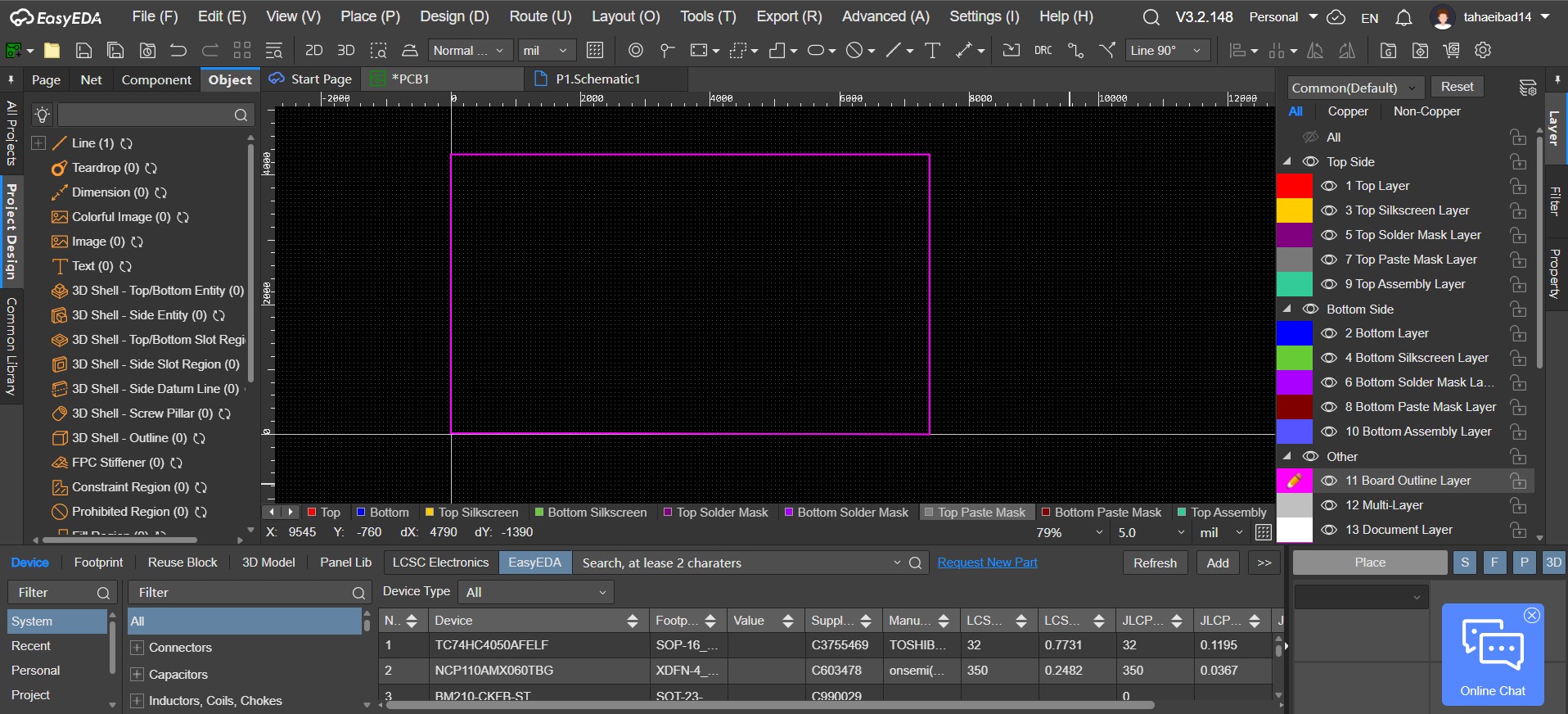
What to define at this stage
- Board outline. Import or draw the exact board shape. If your mechanical engineer has provided a DXF file of the enclosure's PCB cavity, import it directly into EasyEDA (File → Import → DXF) to ensure an exact dimensional match. If you are defining the board shape yourself, use the Board Outline layer to draw the perimeter with precise dimensions.
- Mounting holes. Place mounting holes at the locations specified by your enclosure design. M3 mounting holes typically feature a 3.2 mm drill and a 6.5 mm pad, or a copper keep-out, depending on grounding requirements. Make sure the hole-to-edge clearance meets your fabrication house requirements.
- Keep-out areas. Define regions where no copper, components, or vias may be placed. Common keep-out areas include zones under connectors where mechanical interference could occur, areas near board edges where V-groove panelization or routing will remove material, and regions above and below tall components on the opposite side of the board.
JLCPCB Process Constraint
JLCPCB requires a minimum board-edge-to-copper clearance of 0.3 mm for V-cut panelization and 0.2 mm for tab-routing. Mounting holes should maintain at least 1 mm of annular ring or keep-out clearance from the board edge. The minimum size we can make for a V-cut panel is 70 mm × 70 mm, while the maximum size is 475 mm × 475 mm; otherwise it cannot go through the V-cut machine. Getting the mechanical constraints locked down first prevents the painful scenario of completing a beautiful layout only to discover that the USB connector collides with the enclosure wall, or that a mounting hole lands directly under a BGA package. Measure twice, place once.
2Layer Stackup Design and Design Rules
With your board outline defined, the next decision is how many layers you need and how those layers are organized. This decision is driven by signal density (how many traces need to be routed), impedance control requirements (whether you need controlled-impedance transmission lines), and power distribution complexity (how many voltage rails you need to distribute).
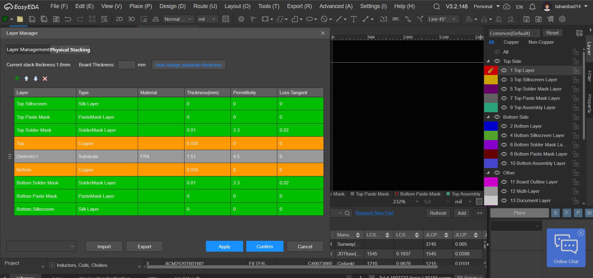
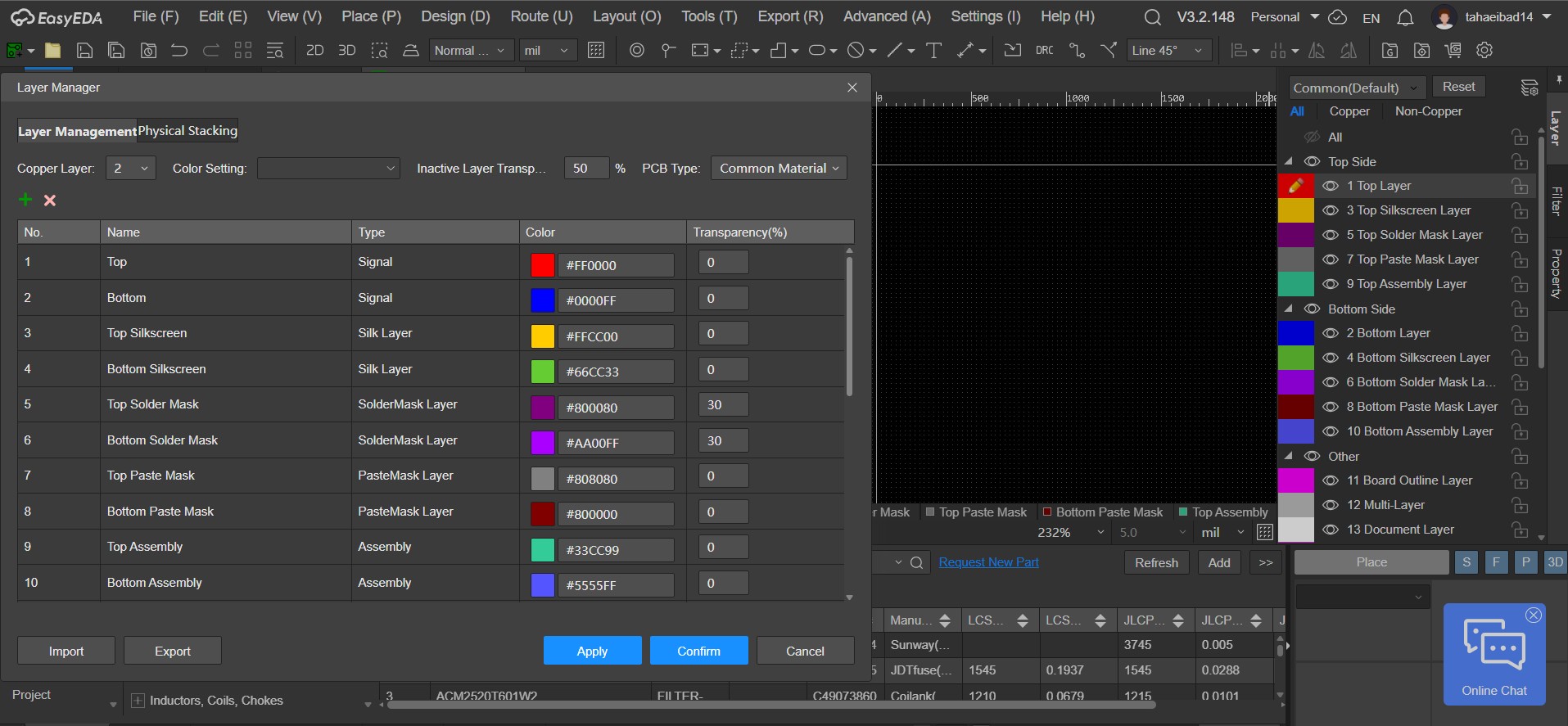
Determining Layer Count
For most designs, the decision follows a practical hierarchy:
- 2 layers — Simple designs with low component density, no controlled impedance requirements, and few high-speed signals. Ideal for breakout boards, simple sensor modules, and low-speed microcontroller applications.
- 4 layers — The sweet spot for medium-complexity designs. Two signal layers (top and bottom) sandwiching a dedicated ground plane. This is the workhorse configuration for most embedded systems, IoT devices, and mixed-signal boards.
- 6+ layers — Typically required for advanced designs, including high-speed digital systems (such as DDR memory and FPGAs), dense BGA fan-out structures, complex power distribution networks requiring dedicated power planes, and RF/microwave applications that require precise layer stackup and controlled electromagnetic coupling.
Configuring Design Rules
Once the stackup is defined, configure the global design rules in EasyEDA that will govern every trace, pad, and via in your design. Navigate to Design → Design Rules and set values that align with your target fabrication process:
| Parameter | JLCPCB Standard (1–2 Layer PCB) | JLCPCB Standard (4+ Layer PCB) |
|---|---|---|
| Minimum Trace Width | 4 mil (0.10 mm) | 3.5 mil (0.09 mm) |
| Minimum Trace Spacing | 4 mil (0.10 mm) | 3.5 mil (0.09 mm) |
| Minimum Via Hole Diameter | 0.15 mm | 0.25 mm |
| Minimum Via Diameter | 0.15 mm | 0.25 mm |
| Minimum Annular Ring | 0.18 mm | 0.15 mm |
| Solder Mask Expansion | 0.09 mm | 0.09 mm |
This is a common rule of thumb: your actual design should treat these as absolute minimums, not targets. A safer default for general routing is 8 mil trace/space, going tighter only where the design demands it (BGA fan-out, fine-pitch QFP routing).
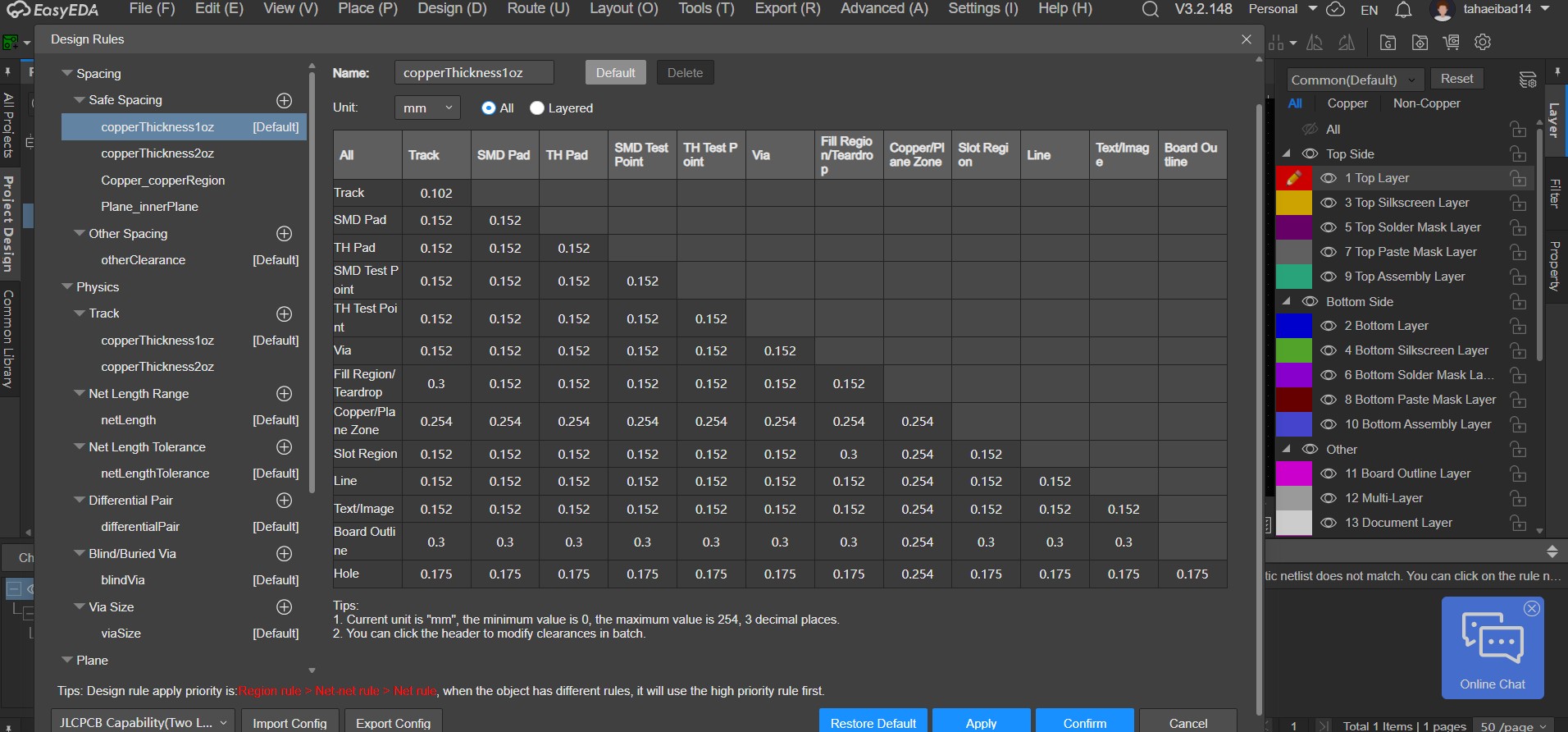
JLCPCB Process Constraint
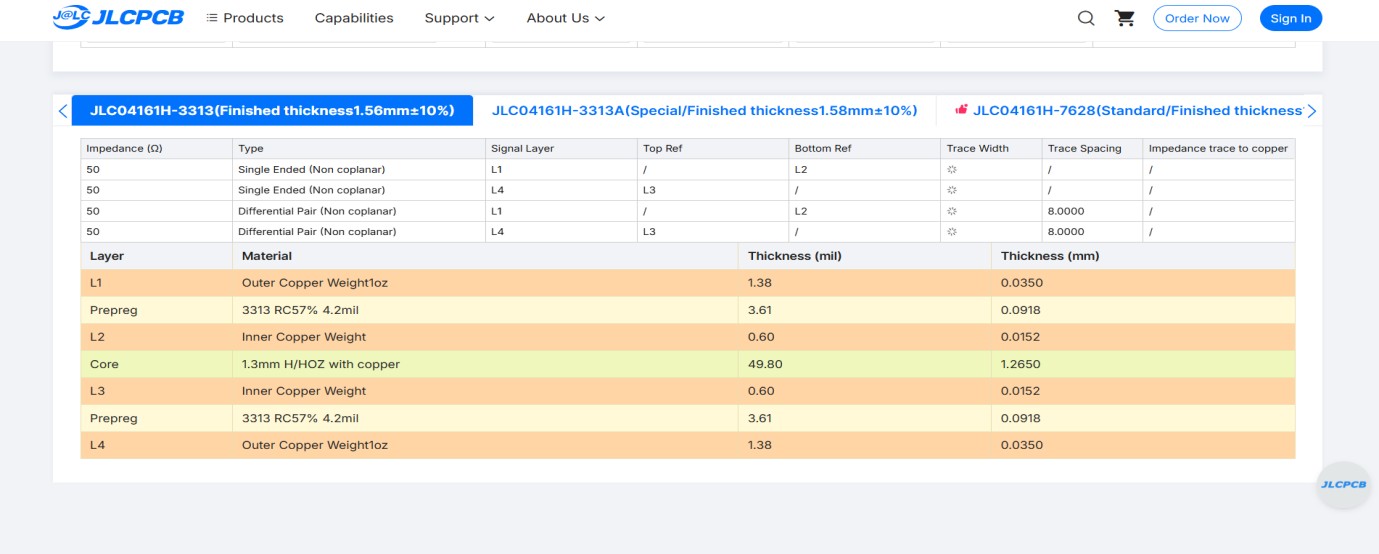
For controlled impedance designs, designers must use JLCPCB's Impedance Calculator to determine the exact trace width required for the target impedance (typically 50 Ω single-ended or 100 Ω differential) based on your selected stackup. Trace widths calculated from generic formulas will not match real production unless they account for the specific dielectric constant and thickness of JLCPCB's materials.
3Power Distribution and Grounding Strategy
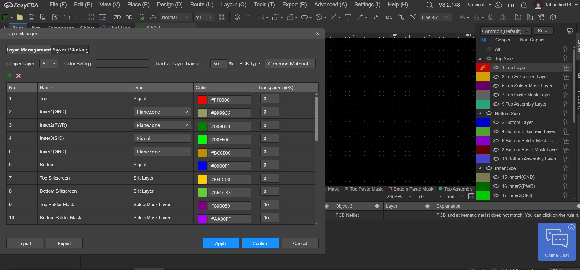
For multi-layer PCB designs (4 layers and above), power and ground planning should be considered early in the layout process. Rather than designing planes separately from component placement, engineers typically perform an iterative optimization between layer allocation, power distribution, and component arrangement.
A preliminary plane strategy helps ensure proper current return paths, minimize power loop areas, and improve signal integrity before detailed routing begins.
Ground Plane: The Non-Negotiable
Every multi-layer PCB needs at least one solid, continuous, uninterrupted ground plane. This is not a suggestion or a best practice—it is a fundamental requirement for signal integrity, EMI performance, and stable power distribution. The ground plane serves as the return current path for every signal on the board, and its continuity directly determines the quality of those return paths.
In a 4-layer stackup, the ground plane typically occupies Inner Layer 1 (immediately below the top signal layer). This placement gives every trace on the top layer an adjacent reference plane, enabling controlled impedance routing and minimizing loop area for high-frequency signals.
Power Plane Planning
The power plane (typically Inner Layer 3 or Layer 4 in a 6-layer board) distributes your supply voltages across the board. If your design has a single voltage rail (e.g., 3.3 V), the entire plane can be dedicated to that rail. If you have multiple rails (3.3 V, 5 V, 1.8 V), the plane must be split into zones—but these splits must be planned carefully to avoid creating slots that cross underneath signal traces.
At this stage, sketch out a rough partition of the power plane based on your circuit's voltage domains. The detailed split boundaries will be refined in Step 4 once you know exactly where each IC and its decoupling capacitors will sit.
JLCPCB Process Constraint
JLCPCB provides free resin-filled, copper-capped via-in-pad (POFV) for all 6–20 layer boards. This is critical for power plane planning in high-density designs because it allows you to place vias directly in component pads that connect to inner power planes, eliminating the need for via-routing detours. For 4-layer boards, standard through-hole vias connecting to inner planes are processed without additional cost.
4Component Layout and Building Blocks Allocation
This is the step where the design truly takes shape—and it is arguably the most impactful step in the entire PCB layout process. A good placement makes routing easy. A poor placement makes routing impossible, no matter how skilled you are with the trace tool.
Importing and Initial Placement
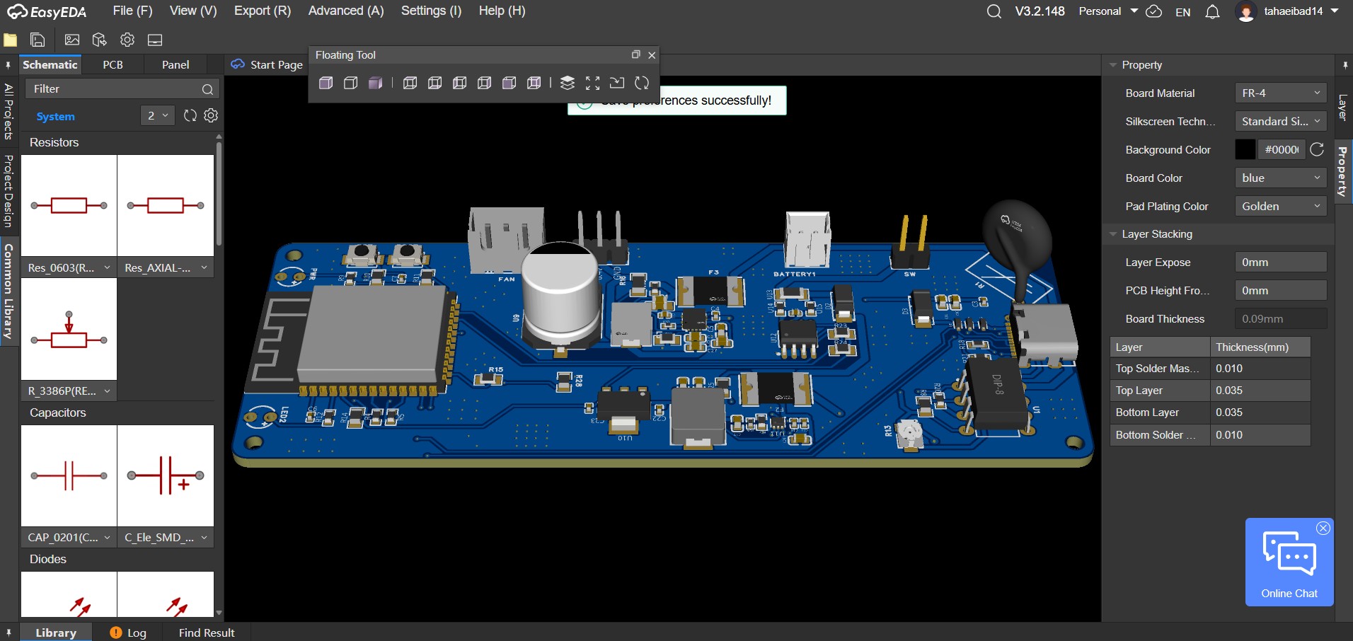
After synchronizing from your schematic, all components appear as a cluster outside the board outline, connected by ratsnest lines. The first task is to drag them onto the board and arrange them into a rough initial placement. Do not worry about perfection yet—the goal is to establish a spatial organization that reflects the circuit's functional architecture.
Functional Block Partitioning
Divide your board into functional zones, just as you divided your schematic into functional sheets. Typical blocks include:
- Power supply section — Input connectors, voltage regulators (LDO/switching), inductors, bulk and bypass capacitors, and protection components (TVS, fuses). Place these near the power input connector and group the switching loop components tightly. For detailed routing and thermal guidelines on power ICs, check out our practical voltage regulator PCB design guide.
- Digital/MCU section — Microcontroller, crystal oscillator, SPI flash, USB interface, debug headers. The crystal and its load capacitors should be placed as close to the MCU's oscillator pins as possible—every millimeter of trace between the crystal and the IC adds parasitic capacitance and degrades oscillation stability.
- Analog/sensor section — ADCs, op-amps, sensor interfaces, voltage references. Isolate physically from the digital and power sections to minimize noise coupling.
- RF section (if applicable) — RF ICs, matching networks, antenna connectors or trace antennas. RF sections demand the most careful placement because impedance-controlled paths are sensitive to even sub-millimeter dimensional changes.
- Connectors and interfaces — Place at board edges in positions that align with the enclosure design and cable routing.
Plane Iteration Based on IC Pin Distribution
Here is where beginners and experienced designers diverge. In high-speed and mixed-signal designs, power plane planning and component placement are not sequential steps—they are iterative. Once you have placed your major ICs and know their actual pin-out positions, go back to the power plane and refine the split boundaries.
For example, if your MCU has VCC pins on pins 7, 18, 32, and 48 (scattered around the package perimeter), the 3.3 V zone of your power plane must extend beneath the MCU to reach all of those pins through short vias. If your ADC requires a separate, quiet analog supply (AVCC), the analog power zone must be positioned directly beneath the ADC with its own dedicated decoupling capacitors placed within 2–3 mm of the AVCC pins.
Decoupling Capacitor Placement
Decoupling capacitor placement deserves special emphasis: every power pin on every IC should have a dedicated bypass capacitor placed as close to the pin as physically possible, with the shortest possible via path to the ground plane. The effectiveness of a decoupling capacitor is dominated by the loop inductance of the path from the cap through the via to the power plane and back through the ground plane to the IC's ground pin. A 100 nF cap placed 20 mm away from the power pin is electrically equivalent to a piece of modern art—decorative, but functionally useless at high frequencies.
JLCPCB Process Constraint
For SMT assembly through JLCPCB's assembly service, ensure that component-to-component spacing meets the minimum clearance for pick-and-place accuracy. JLCPCB recommends a minimum of 0.3 mm between adjacent component bodies for standard SMT assembly. Components placed closer than this may cause placement machine collisions or solder bridging during reflow. Component land patterns should comply with IPC-7351B Nominal density level (Level B) unless your design specifically requires high-density (Level C) packing.
5Critical Signal and Remaining Tracks Routing
With components placed and planes planned, it is time to draw copper. This is the PCB layout design step where everything comes together and where discipline matters most.
Critical Signal Routing: Manual First, Always
The cardinal rule of routing is: route critical signals manually, first, before anything else touches the board. Auto-routers do not understand your circuit—they see nets, not functions. They will happily route your 100 MHz clock signal through a serpentine path under the switching regulator if that happens to be the shortest geometric connection.
The signals that demand manual routing priority are:
- High-speed clocks — Keep traces short, direct, and over an unbroken ground plane. Avoid vias. If a via is unavoidable, place a ground-stitching via within 50 mil to provide a return current path.
- Differential pairs — Route as tightly coupled pairs with consistent spacing. Match trace lengths to within the tolerance specified by the interface standard (e.g., ±5 mil for USB 2.0). Use EasyEDA's differential pair routing tool to enforce coupling and length matching automatically.
- Sensitive analog signals — Low-level sensor inputs, reference voltage dividers, feedback networks for voltage regulators. Guard these with ground pour or guard traces and keep them physically separated from digital switching noise.
- Power switching loops — The high-current loop in a switching regulator (input cap → switch node → inductor → output cap → return) is not a "signal," but it must be routed with the same care. Minimize the loop area by keeping these components tight and using wide, short traces or copper pours.
Remaining Routing: Complete the Connections
After all critical nets are routed, the remaining low-speed, non-critical signals (GPIO, LED indicators, button inputs, I2C/SPI at moderate speeds, configuration pins) can be routed. Depending on your design complexity and personal preference, you have two approaches:
- Manual routing — Gives you full control over trace paths and is recommended for designs where board density is moderate and you can complete routing in a reasonable time.
- Assisted auto-routing — For boards with many low-speed connections, EasyEDA's auto-router can handle the remaining nets. However, always perform a thorough manual review after auto-routing. Look for unnecessarily long trace paths, traces that run parallel to critical signals (potential crosstalk), vias that could be eliminated, and traces that cross ground plane splits.
After all nets are routed, run a Design Rule Check (DRC) to verify that every connection is made, every clearance is met, and every trace width satisfies the configured minimums. Fix all violations and re-run until you achieve a clean DRC pass.
JLCPCB Process Constraint
Guidelines for both trace width (versus current capacity) and general trace spacing are covered in IPC-2221: Generic Standard on Printed Board Design. As a conservative reference for practical scenarios, a 1 mm/30 mil trace is preferred to carry 1 A, though actual capacity depends on various shifting factors; while clearance requirements are defined based on voltage differentials and conductor location.
Advanced PCB Layout Best Practices
Design for Manufacturability
Your PCB design exists in a simulation environment until the moment you submit it to a fabrication house. At that point, every dimension, every clearance, and every drill hole must be producible with real machines operating at real tolerances. Designing a board that looks perfect in your EDA tool but violates your manufacturer's capabilities will result in production failure.
Design for Manufacturability (DFM) means designing with your manufacturer's specific production limits in mind from the start—not as an afterthought check at the end. This includes trace width and spacing minimums, minimum annular ring sizes, solder mask dam widths (the bridge of solder mask between adjacent pads, typically 0.2 mm minimum for JLCPCB), silkscreen-to-pad clearance, and via-to-pad clearance.
By choosing JLCPCB's PCB Layout Service, DFM checks are automatically performed at this stage to ensure your design meets JLCPCB's production capabilities. The experienced layout engineers know the exact manufacturing tolerances of JLCPCB's production lines—including edge cases that generic DRC rules do not cover—guaranteeing that the delivered files are ready for fabrication and can go straight into production without rework or re-spins. For complex designs where DFM compliance is as important as electrical performance, this service removes the guesswork entirely.
Securing Signal Integrity and Minimizing Crosstalk
Signal integrity problems rarely announce themselves with a clean error message. Instead, they manifest as intermittent glitches, marginal timing failures, unexpected EMI emissions, and the infamous "it works on my bench but fails in production" syndrome. The PCB layout best practices that prevent these issues are well-established, and they cost nothing to implement if you build them into your workflow from the start.
- Avoid long parallel runs between signal traces. When two traces run parallel and adjacent to each other for more than a few millimeters, capacitive and inductive coupling between them transfers energy from one trace to the other—this is crosstalk. The longer the parallel run, the worse the coupling. If two traces must travel in the same direction, stagger their routing or insert a ground trace (or ground pour) between them as a shield.
- Route signals on adjacent layers perpendicularly. If you have signal traces on the top layer running horizontally, the traces on the bottom layer should run vertically (or at least at a significant angle to the top layer traces). This minimizes the overlap area between traces on different layers, reducing interlayer capacitive coupling. This perpendicular routing convention is one of the oldest and most effective PCB layout best practices in the book.
- Protect the ground plane. Every slot, split, or gap in the ground plane is a potential impedance discontinuity for any signal trace that crosses it. A return current flowing through the ground plane beneath a signal trace will be forced to detour around any gap, increasing the loop area and creating an unintentional antenna. The rule is simple: never route signal traces over ground plane splits or slots. If a split is necessary (for analog/digital isolation, for example), ensure that no signal traces cross the boundary.
Effective Thermal Management
Heat is the silent killer of electronics. Every component on your board dissipates power, and that power becomes heat. If the heat is not managed—conducted away from the component, spread across the copper, and ultimately dissipated to the environment—junction temperatures rise, component lifetimes decrease, and reliability drops.
PCB layout best practices for thermal management include:
- Thermal vias under high-power components. For components with exposed thermal pads (QFN packages, power MOSFETs, voltage regulators), place an array of thermal vias directly beneath the thermal pad, connecting it to a large copper pour on an inner layer or the opposite side of the board. A typical pattern is a 3×3 or 4×4 grid of 0.3 mm vias on a 1.0–1.2 mm pitch. These vias conduct heat from the component through the board thickness, dramatically reducing thermal resistance.
- Copper pour for heat spreading. Large areas of copper on the top and bottom layers act as heat spreaders, distributing thermal energy over a wider area for convective and radiative dissipation. Connect these copper pours to the ground or power planes through multiple vias to create a continuous thermal path from the component to the largest possible copper area.
- Reserve space for heatsinks. If your design includes components that dissipate significant power (linear regulators, power amplifiers, motor drivers), reserve physical space above those components for clip-on or adhesive heatsinks during the placement phase. Nothing is more frustrating than completing a perfect layout only to discover that the heatsink for your 2 W LDO collides with a neighboring tall electrolytic capacitor. Plan for thermal solutions during placement, not after routing.
FAQ about PCB Layout Process
Q: How long does the PCB layout process typically take?
It depends entirely on complexity. A simple two-layer board with 20–30 components can be laid out in a few hours by an experienced designer. A four-layer mixed-signal board with 100+ components, controlled impedance requirements, and multiple power rails typically takes 2–5 days of focused work. High-density designs with BGA packages, DDR routing, or RF sections can take weeks. The key variable is not the number of components but the number of critical constraints—impedance control, length matching, thermal management, and DFM requirements all add time. Rushing the PCB layout process to save a day almost always costs you a week in debugging and re-spins.
Q: Should I design my PCB in 2 layers or 4 layers?
If your design has any of the following characteristics, go with 4 layers: high-speed signals above 25–50 MHz, controlled impedance requirements, a switching power supply on-board, mixed analog and digital sections, or more than moderate component density. The cost difference between a 2-layer and 4-layer prototype at JLCPCB is modest, and the design benefits are substantial—dedicated ground and power planes dramatically improve signal integrity, simplify routing, reduce EMI, and make the entire PCB layout design process more straightforward. Two-layer boards are perfectly suitable for simple, low-speed designs where cost optimization is the priority.
Q: What are the most common PCB layout mistakes that cause first-spin failures?
Three mistakes account for the majority of first-spin failures. First, incorrect or mismatched component footprints—the schematic symbol connects to a footprint that does not match the physical part, resulting in a board that cannot be assembled. Always verify footprints against datasheets and order standards like IPC-7351B before manufacturing. Second, inadequate decoupling—either missing bypass capacitors or placing them too far from their associated IC power pins, leading to noisy power rails and unstable operation. Third, ground plane violations—routing signal traces over splits, slots, or gaps in the ground plane, creating unintended impedance discontinuities and EMI radiation. Follow the PCB layout best practices outlined in this article, and you will avoid all three.
Q: Can I rely on auto-routing for my entire PCB design?
For professional designs, the honest answer is no—not for the entire board. Modern auto-routers (including EasyEDA's) have improved significantly and can produce acceptable results for low-speed, non-critical connections. However, auto-routers do not understand circuit function. They cannot distinguish between a 100 MHz clock net and an LED indicator net—they treat both as simple point-to-point connections to be optimized for shortest path. The recommended approach is to manually route all critical signals first (clocks, differential pairs, power loops, sensitive analog), and then use auto-routing for the remaining non-critical connections, followed by a thorough manual review and cleanup. This hybrid approach gives you the reliability of manual routing where it matters and the speed of auto-routing where it is safe.
Q: How do I know if my design is ready to send to the fabrication house?
Run through this five-point check before submitting. First, DRC passes with zero errors. Second, all nets are routed (no remaining ratsnest lines). Third, the board outline is a closed shape on the correct layer. Fourth, silkscreen text does not overlap pads and is legible at the font size you used. Fifth, open the Gerber files in a standalone viewer (like the JLCPCB Gerber viewer) and visually inspect each layer—check that copper pours look correct, drill holes are where you expect them, and solder mask openings match your pad locations. This final visual inspection catches issues that automated DRC cannot: missing copper fills, cosmetic silkscreen problems, and layer alignment errors. Five minutes of visual review can save five days of waiting for boards that are wrong.
Conclusion about PCB Layout Process
The PCB layout process is a disciplined sequence of decisions—each one building on the last—that transforms an abstract schematic into a physical board ready for manufacturing. From defining the mechanical envelope and selecting the right layer stackup, to planning power and ground planes, partitioning the board into functional blocks, and routing critical signals before the general wiring, every step has a direct and measurable impact on the performance, reliability, and manufacturability of the final product.
There are no shortcuts in this process. A well-executed PCB layout process does not guarantee a perfect product, but a poorly executed one guarantees problems. The engineers who consistently produce boards that work on the first spin are not luckier than you—they are more disciplined. They verify footprints against datasheets, they check their stackup against the manufacturer's materials, they route clocks before LEDs, and they run DRC before they celebrate.
Master the process. Trust the process. And when the process reveals an error—fix it before it becomes five hundred errors on five hundred boards. Alternatively, if your team lacks the bandwidth to manage this rigorous pipeline, leveraging a professional JLCPCB layout service can ensure these strict standards are met from day one.
Keep Learning
How to Design a PCB Board: 5 Steps from Schematic to Layout
Designing a PCB board means turning a validated schematic into a manufacturable layout: start with a clean schematic, place components by function and signal flow, route traces with signal integrity in mind, then manage heat and EMI before running design rule checks and exporting Gerber files. Free tools like EasyEDA cover the complete workflow. This guide explains the layout guidelines that matter at each stage, from schematic preparation to thermal management. Introduction Printed circuit board (PCB......
EMI vs EMC: A Full Guide to Detailed Comparison
EMI (electromagnetic interference) is unwanted electromagnetic energy that degrades the performance of electronic devices. EMC (electromagnetic compatibility) is the design discipline that ensures a device works properly in its electromagnetic environment without disturbing other equipment. For PCB designers, the distinction matters because every layout decision — stackup, grounding, component placement, and trace routing — determines how much EMI a board emits and how well it survives it. Introductio......
PCB Design Guidelines 101: Placement and Routing
Welcome to the second article in our PCB design guidelines series. In this article, we will explore the essential PCB design guidelines that are crucial for achieving optimal PCB design performance and functionality. Whether you're an electronics enthusiast, hobbyist, engineer, student, or professional in the field, understanding these guidelines will empower you to create high-quality PCB designs. In this article we will explore foundational principles and best practices in designing printed circuit ......
BGA PCB Design Complete Guide: Layout and Routing Guidelines
Key Takeaways Define pad type first: Always confirm SMD or NSMD pad strategy before routing BGA fanout. NSMD is generally preferred for better solder joint formation, while SMD suits very small pads or tight mask registration. Match the process to the pitch: 0.8 mm BGAs work with dog-bone fanout and standard vias; 0.5 mm BGAs typically need via-in-pad or HDI routing. Picking the right via strategy early saves layers and cost. Place decoupling capacitors on the bottom side: Mount MLCCs directly under t......
The Ultimate Guide to PCB Layout Design
Printed Circuit Board (PCB) layout design is the foundation of any electronic device, from simple gadgets to highly complex systems. PCB layout design is the process of arranging electronic components and routing connections on a board to create a functional and efficient circuit. The goal is to achieve the smallest possible footprint while maintaining signal integrity and ensuring thermal and electrical performance. There is a lot that goes into any engineered circuit board design, from a basic print......
PCB Layout Guidelines for USB Type-C
Introduction to USB Type-C USB Type-C (USB-C) is a universal connection standard used for device connectivity and charging. As the latest evolution of USB interface, USB-C comes with several advantages, including reversible plug orientation, higher data transfer rates, and power output capabilities. Additionally, USB Type-C can transmit audio and video signals and is compatible with various accessories such as monitors, external storage devices, and chargers. Features of USB Type-C Reversible Plug Ori......