Circuit Board Ground Plane and Power Plane Guide 2026
25 min
- Ground Plane PCB Design: Core Principles
- Power Planes in PCB Design: Layout Best Practices
- Ground Plane Design for High-Speed and Mixed-Signal PCBs
- Common PCB Power Plane Mistakes and How to Avoid Them
- FAQ about Circuit Board Ground Plane Design
- Conclusion about Circuit Board Ground Plane
Key Takeaways
Continuous copper first: A solid circuit board ground plane creates a low-impedance return path, reduces noise, and is usually safer than split planes, even on mixed-signal boards.
Think in current loops: Every signal needs a return path directly beneath it. Never route high-speed traces across plane gaps, slots, or cutouts.
Plan the stack-up early: Choose the layer arrangement before routing critical signals, and keep power and ground planes close together to lower distribution inductance.
Placement beats filtering: Short decoupling loops, well-positioned stitching vias, and careful component grouping prevent most EMI and ground-loop problems.
Verify before fabrication: Rebuild copper pours, run DRC, inspect Gerbers, and match the stack-up and copper weight with the manufacturer's actual capabilities.
A well-designed circuit board ground plane does more than provide a convenient connection to ground. It creates a low-impedance return path, reduces unwanted voltage differences across the board, and helps control noise generated by high-speed signals and switching circuits. The same principle applies to the power plane in PCB layouts, where stable current delivery and low distribution impedance directly affect circuit reliability.
Poorly planned planes can create long return paths, ground loops, voltage drop, electromagnetic interference, and unexpected signal-integrity problems. These issues become more serious when a board includes fast digital interfaces, sensitive analog sections, switching regulators, or several voltage rails. Ground and power copper also contribute to thermal management by spreading heat away from high-current components and reducing localized hot spots.
This guide explains practical ground plane PCB design, return-path planning, via stitching, layer stack-up selection, decoupling capacitor placement, and multi-voltage plane segmentation. For dense or complex boards, the JLCPCB Layout Service can also support component placement, routing, and fabrication-aware PCB layout based on a completed schematic.
Ground Plane PCB Design: Core Principles
A common mistake in PCB layout is to treat the ground plane as something that can be added after the routing is finished. In practice, the plane should influence placement and routing from the beginning. A trace may look correct on the signal layer while its return current is forced to take a long route underneath it. That hidden return path is often the real source of noise, ringing, or unexpected EMI problems.
Good ground plane PCB design starts by deciding which copper layer will provide the main reference for critical signals. High-speed traces should remain over continuous copper, without passing across gaps, slots, or disconnected regions. When the reference plane is interrupted, return current has to move around the opening. This increases the loop area and adds inductance to the path.
The plane also needs to be checked after routing. Clearances around pads, vias, and board edges can leave narrow copper sections or isolated islands that are easy to miss in the editor. These details may not cause an immediate design-rule error, but they can still affect current flow and noise performance.
Plane Design Quick Checklist
Use this checklist before completing the first routing review:
- Keep the main ground region as continuous as the layout allows.
- Check what lies underneath every high-speed or clock trace.
- Do not route critical signals across plane gaps or cutouts.
- Place decoupling capacitors close to the related power pins.
- Add nearby ground vias when a signal changes layers.
- Look for narrow copper necks and isolated copper islands.
- Rebuild the copper areas and run DRC after major layout changes.
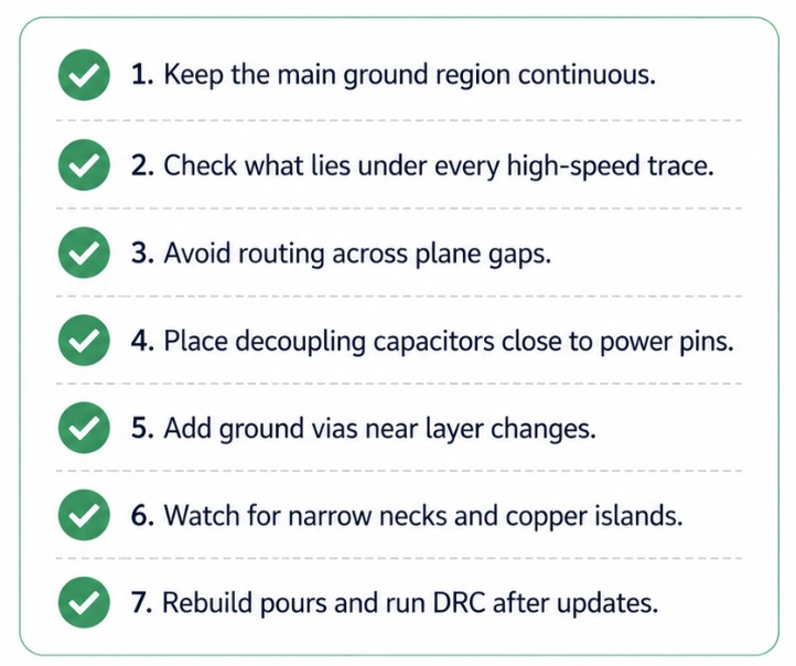
Ground plane PCB design quick checklist.
Solid vs. Split Ground Planes
A solid ground plane is usually the safest starting point for most PCB layouts. It gives signal return current a continuous path and reduces the chance of unexpected detours around gaps or narrow copper sections. This is especially important for clocks, communication lines, and other fast signals, where return current tends to remain close to the signal trace.
A split ground plane divides the copper into separate regions. Designers sometimes use this approach to keep noisy switching circuits away from sensitive analog sections. The problem appears when a signal trace crosses the gap between those regions. The signal may travel directly across the board, but its return current cannot pass through the missing copper. It must move around the split, increasing the loop area and making the board more likely to suffer from noise or EMI.
For that reason, splitting the ground plane should not be the automatic solution for mixed-signal boards. In many cases, one continuous plane with careful component placement works better. Keep switching converters, digital processors, and sensitive analog circuits in their own physical areas, then control how current flows between them.
If a split is genuinely required, do not route critical signals across it. Check the component manufacturer's grounding recommendations and decide where the separate regions should connect. Good ground plane design depends on the complete current path, not only on the shape of the copper.
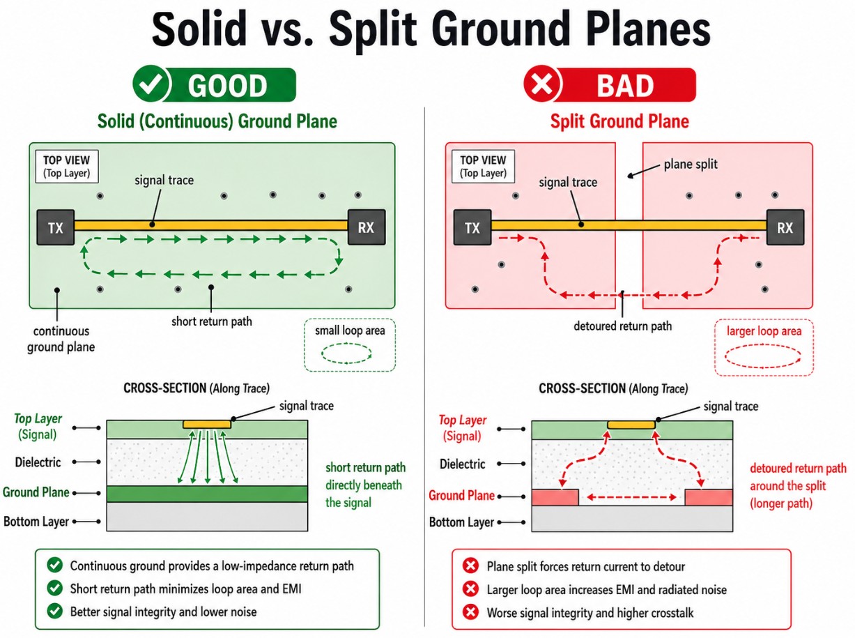
Solid and split ground planes with return paths.
Return Path Planning
A signal trace is only half of the current path. The current must also return to the source, usually through the nearest ground reference. This second path is easy to overlook because it is not drawn as a visible trace on the signal layer.
On a well-planned board, the return current can flow through the ground plane directly beneath the signal. The outgoing and returning currents remain close together, which keeps the loop area small. Problems appear when the trace passes over a slot, plane boundary, or isolated copper region. The signal continues across the opening, but its return current must travel around it. A trace that looks short in the PCB editor can therefore create a surprisingly large current loop.
This issue deserves particular attention around connectors and signal vias. When a signal changes layers, its reference plane may also change. A nearby ground via gives the return current a short path between the two ground regions. Without that connection, the return current may travel through a distant via, connector pin, or decoupling capacitor before reaching the correct reference plane.
During layout review, inspect the copper beneath clock lines, USB signals, communication buses, and switching nodes. Do not judge the route by the signal trace alone. Follow the complete loop from the driver to the receiver and back to the source.
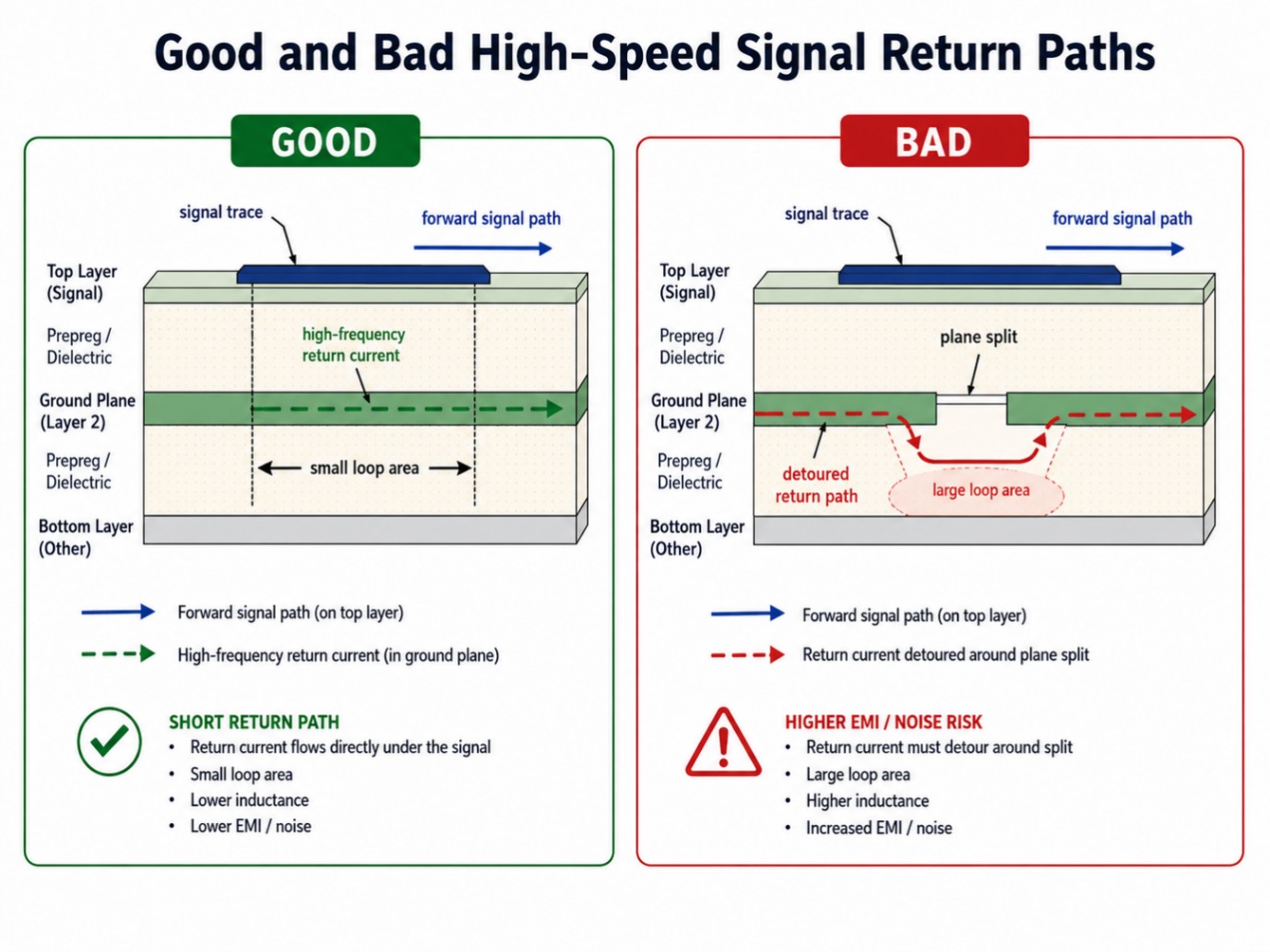
Good and bad high-speed signal return paths.
Texas Instruments High-Speed Layout Guidelines explains that a slot in the reference plane forces return current onto a different route, increasing the current-loop area.
Via Stitching Strategies
Ground stitching vias are most useful when they are placed for a clear electrical reason. Filling every open area with vias may look thorough, but location matters more than quantity. The first places to inspect are signal-layer transitions, board edges, and boundaries around noisy or sensitive circuits.
When a high-speed signal changes layers, its return current may need to move between reference planes as well. A ground via positioned close to the signal via gives that current a short connection between the planes. When the ground via is too far away, the return current has to travel across the board before it can follow the signal again. That larger path adds inductance and can increase noise.
Via stitching is also useful around board edges, RF sections, switching converters, and shielded areas. A row of grounded vias can connect copper on several layers and reduce the chance that the board edge behaves like an unintended radiator. The same technique can help contain current around fast switching loops, although it cannot compensate for poor component placement or fragmented ground copper.
Check the copper after adding the vias. Clearances around pads and traces may create narrow sections that are difficult to notice at normal zoom. Rebuild the copper pour, inspect the connections, and run DRC before considering the section complete. EasyEDA PCB Tools includes tools for adding and removing vias between overlapping copper regions that use the same net.
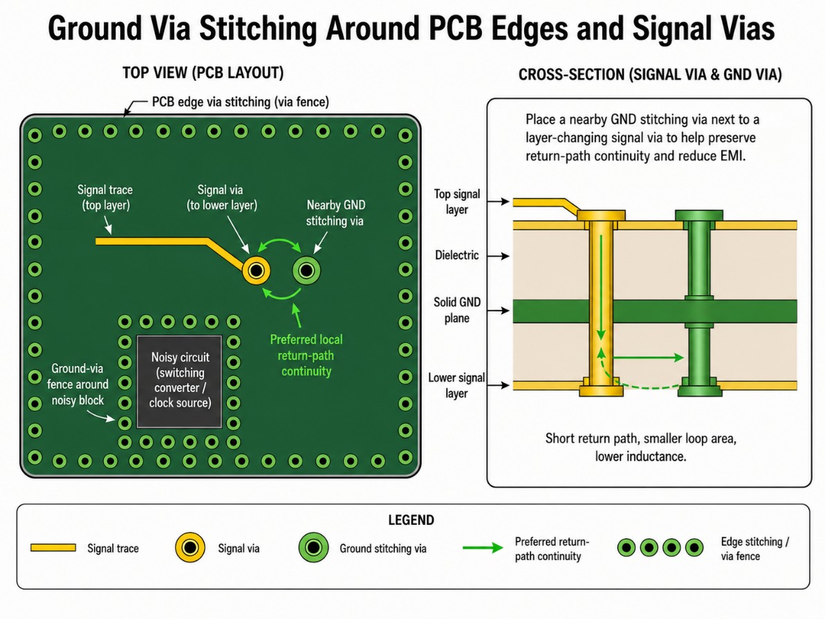
Ground via stitching around PCB edges and signal vias.
Power Planes in PCB Design: Layout Best Practices
A power plane may look like a simple copper area, but its shape has a direct effect on voltage stability, heat, and noise. The connection can be electrically correct in the schematic while still performing poorly on the finished board. This usually happens when supply current is forced through a narrow copper neck, a long route, or a group of vias that was not sized for the expected load.
Good power planes in PCB design should provide a short and reasonably wide path from the power source to each load. The copper needs to be checked around connectors, regulator outputs, large capacitors, mounting holes, and dense component areas. Clearances around pads and traces can remove more copper than expected, leaving a weak section that is easy to miss at normal zoom.
The power plane in PCB layouts must also be considered together with the ground plane. When power and ground layers are placed close to one another, the current loop between them becomes smaller and the power-distribution path has lower inductance. This helps the decoupling capacitors respond more effectively when an IC suddenly demands current.
The final geometry still depends on copper thickness, board thickness, dielectric spacing, current level, and the selected manufacturing stack-up. Before locking the design, compare the layer arrangement with JLCPCB Multi-Layer PCB Standard Laminated Structures. Controlled-impedance traces should also be checked using the JLCPCB PCB Impedance Calculator rather than relying on a generic stack-up value.
Layer Stack-Up Arrangement
The stack-up should be selected before routing clocks, communication buses, or controlled-impedance traces. Changing the layer order near the end of the project can alter trace impedance and leave critical signals referencing the wrong copper layer.
A practical four-layer board often uses the following arrangement:
- Top layer — components and signal routing
- Inner layer 1 — continuous ground plane
- Inner layer 2 — power regions and slower signals
- Bottom layer — signal routing
This arrangement gives top-layer signals a nearby ground reference. It also provides a dedicated internal layer for the main supply rails. However, the third layer may contain several separate voltage regions, so bottom-layer signals must be reviewed carefully. A fast signal should not travel above a gap between two power regions.
A six-layer board offers more control. One useful arrangement is:
- Top signal
- Ground plane
- Internal signal
- Power plane
- Ground plane
- Bottom signal
The second ground layer provides a nearby reference for bottom-layer routing and makes some signal transitions easier to manage. This is an example rather than a universal solution. Dense BGA routing, RF circuits, fast memory interfaces, and high-current sections may require a different order.
The selected construction must match what the PCB manufacturer can build. Dielectric thickness and copper weight affect impedance, so trace dimensions should not be finalized before checking the manufacturer's actual stack-up. EasyEDA Layer Manager can be used to configure the copper-layer count and organize the ground, power, and signal layers inside the PCB editor.
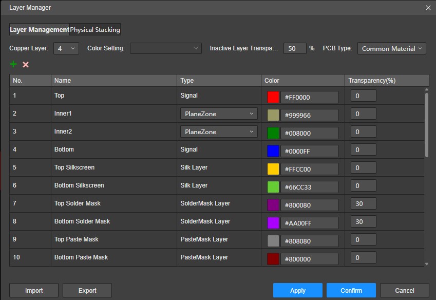
Four-layer PCB stack-up configuration in EasyEDA.
Decoupling Capacitor Placement
A decoupling capacitor works best when the current loop between the capacitor, the IC power pin, and the ground plane is kept small. The capacitor value matters, but poor placement can prevent even a correctly selected part from responding effectively to fast changes in current.
Place the capacitor beside the related power pin rather than somewhere within the general area of the IC. The connection from the capacitor to the pin should be short and direct. On the ground side, place a ground via close to the capacitor pad so the return current can enter the ground plane without travelling along a long trace.
A common layout mistake is to connect the power trace to the IC first and then branch off toward the capacitor. In that arrangement, the capacitor sits at the end of a side path and is less effective at supplying fast transient current. A better route passes through or immediately beside the capacitor connection before reaching the IC power pin.
Large bulk capacitors still have a role, especially near regulators, connectors, and circuits with sudden load changes. However, they do not replace the small local capacitors positioned next to individual IC power pins. Each type handles a different part of the frequency range and current demand.
After placement, inspect the complete loop rather than measuring only the distance between the capacitor and the IC. Long ground traces, distant vias, and narrow copper connections can increase inductance even when the components appear close together.
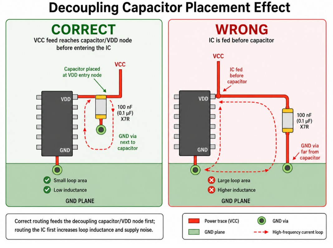
Correct and wrong decoupling capacitor placement.
Plane Segmentation for Multi-Voltage Boards
Multi-voltage boards often need separate copper regions for rails such as 1.2 V, 1.8 V, 3.3 V, and 5 V. The difficult part is not drawing the regions. It is making sure each rail reaches its loads without creating narrow copper necks, accidental islands, or gaps beneath important signal traces.
Start by grouping components according to the rail they use. This makes the power regions easier to define and reduces the number of awkward connections between different parts of the board. Regulators, bulk capacitors, and high-current loads should be placed so the main current path is short and easy to inspect.
Each copper region should be assigned to the correct net before the pour is rebuilt. After that, zoom in around vias, pads, mounting holes, and component clearances. A power region may look large overall while one small connection carries all the current into the area. That narrow section can create voltage drop and local heating.
Do not route high-speed or clock signals across the boundary between two power regions unless a continuous ground plane remains directly beneath them. A signal crossing a split reference can force its return current to take a longer path and increase noise.
Before release, rebuild every copper area, run DRC, and inspect the Gerber output. JLCPCB Instructions for Ordering can be used to check fabrication requirements before uploading the final files.
Multi-voltage segmentation is one of the easiest places to make a layout mistake. A misplaced boundary or weak copper connection may not be obvious until the board is powered. For designs with several rails or dense routing, the JLCPCB Layout Service can support placement, routing, and fabrication-aware layout based on the completed schematic.
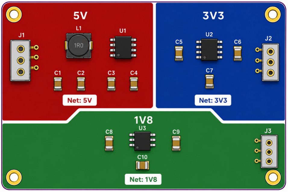
Multi-voltage power plane segmentation in EasyEDA.
Ground Plane Design for High-Speed and Mixed-Signal PCBs
High-speed and mixed-signal boards often fail because the layout is divided by circuit type without considering where the current actually flows. A board may have clearly marked analog, digital, and power sections, yet still suffer from noise if their return paths overlap or cross sensitive areas.
Good ground plane design starts with placement. Keep noisy switching circuits, processors, clocks, and communication interfaces away from low-level analog inputs. The goal is not simply to draw separate boxes around each section. The goal is to control where current enters the board, where it returns, and which parts of the plane it passes through.
Fast digital signals need a continuous reference plane beneath their routes. Sensitive analog signals need protection from switching currents and large voltage changes in nearby copper. Mixed-signal components, such as ADCs and DACs, require extra attention because their analog and digital pins may share the same package while serving very different current paths.
The component datasheet should be treated as the first reference when deciding how these grounds should connect. Some devices work best with one continuous plane and careful placement. Others recommend controlled separation or a connection at a specific point beneath the component.
Analog vs. Digital Ground Separation
Separating analog and digital grounds is often presented as a standard rule, but it is not automatically the best choice. A poorly planned split can create a longer return path and force signals to cross a gap in the reference plane.
A more reliable approach begins with component placement. Keep analog components together and place digital circuitry in a separate physical area. Route analog signals within the analog section and digital signals within the digital section. This limits the chance that fast switching current will pass through sensitive analog copper.
On many boards, one continuous ground plane works well when the sections are placed carefully. The continuous copper gives return current a direct path and avoids the discontinuities created by a split. The important point is to prevent digital current from flowing through the analog area.
A split may still be appropriate when the component manufacturer specifically recommends it or when isolation is required by the system. In that case, the two regions should connect at a controlled location. Signals should not cross the split unless their return path is also provided at the same point.
Before making the final decision, check the grounding recommendations for ADCs, DACs, amplifiers, sensors, and isolated interfaces. The correct arrangement depends on the device, signal bandwidth, current path, and board architecture.
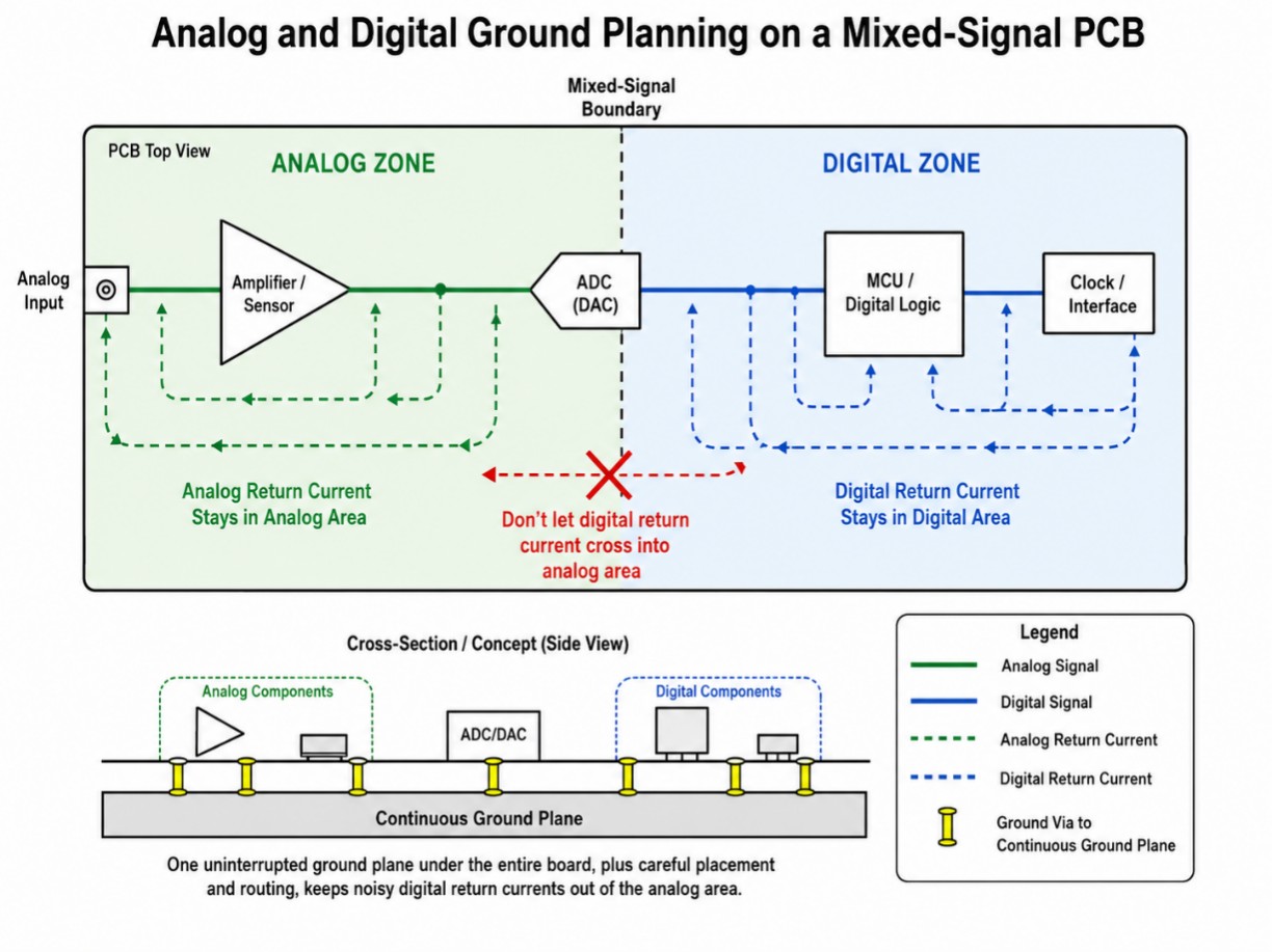
Analog and digital ground planning on a mixed-signal PCB.
Avoiding Ground Loops
A ground loop appears when current has more than one path back to its source. On the PCB itself, the problem may be small. Once cables, shields, external power supplies, test equipment, or chassis connections are added, the complete system can form a much larger loop.
The loop becomes troublesome when the two ground points are not at exactly the same voltage. Even a small difference can drive current through the cable shield or signal ground. That current adds unwanted voltage to sensitive measurements and may appear as hum, noise, unstable sensor readings, or communication errors.
Ground loops are common in systems where two powered boards are connected by a grounded cable. Each board already has a return path through its own supply, while the cable creates another connection between them. Connecting a PCB to an oscilloscope or grounded computer can also introduce a path that was not present during the original design.
The solution depends on the complete system rather than one copper shape. Review every connection to protective earth, chassis, cable shield, power return, and external equipment. Low-frequency analog systems may benefit from a controlled single-point connection. High-frequency designs often need short, low-impedance chassis connections near the connector instead of a long wire running across the board.
Cable shields should also be handled deliberately. Leaving a shield floating can reduce its effectiveness, while connecting it at several distant points may create unwanted current flow. The correct approach depends on the cable type, frequency range, safety requirements, and whether the product is connected to protective earth.
Before releasing the layout, draw the full return path outside the PCB as well as inside it. Many ground-loop problems are created by connectors and cables, not by the ground plane alone.
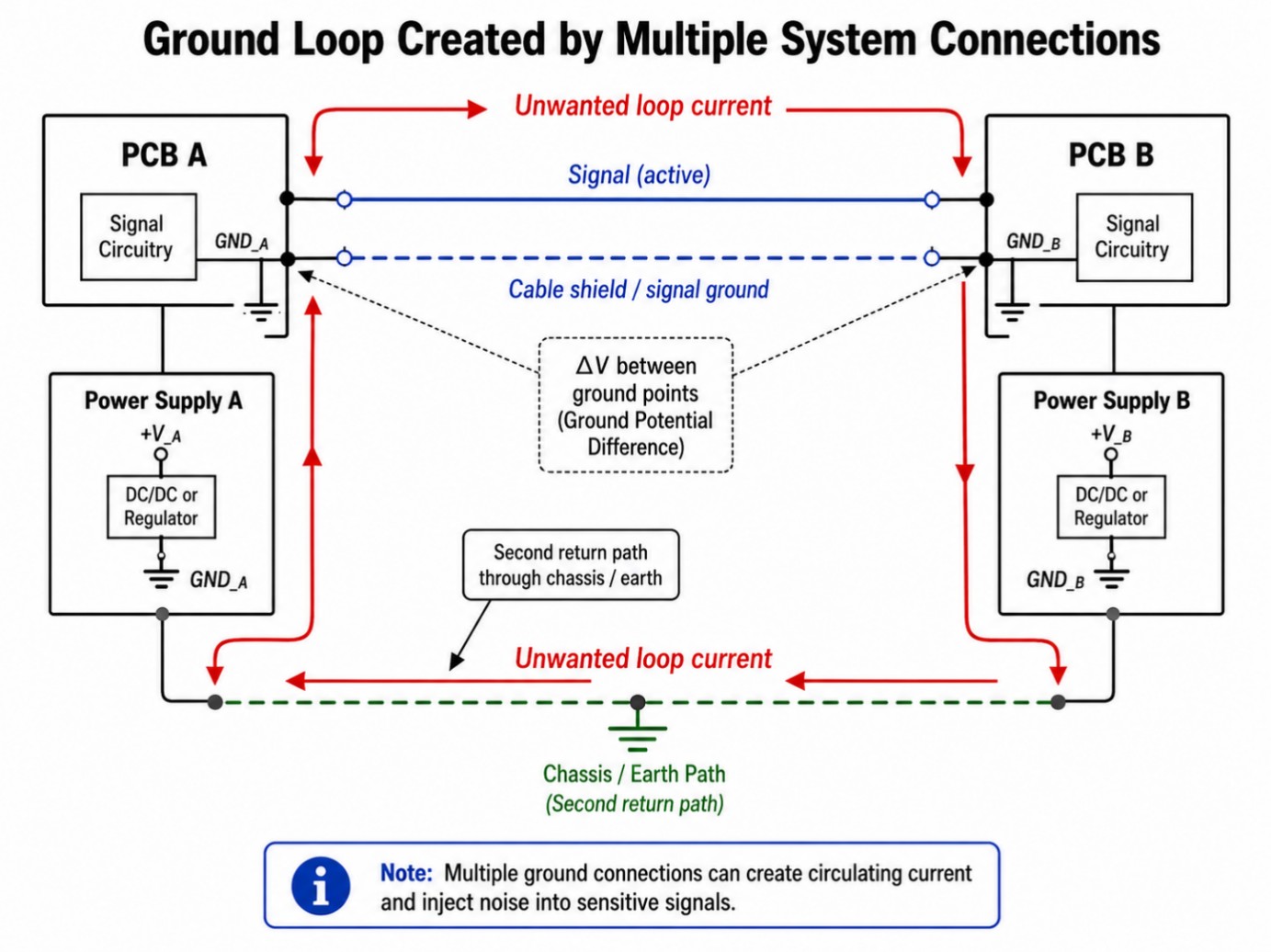
Ground loop created by multiple system connections.
EMI Shielding Considerations
EMI control starts with current-path control. A metal shield or grounded copper area can help, but it will not fix a layout where fast switching current is allowed to spread across the board. The first priority is to keep noisy loops small and provide a continuous return path close to each high-frequency signal.
Connect shield cans to ground at several short points around their perimeter. A long, narrow connection adds inductance and reduces the shield's effectiveness at higher frequencies. Ground stitching vias placed around the shield boundary can connect the top copper to the internal ground plane and help prevent current from escaping through gaps.
Connectors deserve the same attention. Noise entering or leaving through a cable should be returned to chassis or ground close to the connector rather than routed across the PCB first. Protection components, common-mode filters, and shield connections are usually most effective near the point where the cable enters the board.
Board-edge stitching can also reduce radiation from the edges of multilayer boards. The vias should connect ground copper on the outer layers to the main internal ground plane. However, adding a dense row of vias is not a substitute for good placement, short switching loops, or a continuous reference plane.
Avoid leaving isolated copper areas near high-speed sections. A floating copper island may behave unpredictably and can couple noise into nearby traces. If extra copper is kept, connect it deliberately to ground with suitable vias and confirm that it does not interfere with controlled-impedance routing.
During the final review, inspect switching regulators, clock sources, fast digital interfaces, cable connectors, and shield boundaries together. EMI problems usually come from the complete current loop, not from one trace viewed in isolation.
Common PCB Power Plane Mistakes and How to Avoid Them
Power-plane problems are not always obvious during routing. The copper may be connected to the correct net and the design may pass DRC, yet the finished board can still suffer from voltage drop, noise, or local heating. These failures usually come from the shape of the copper rather than a completely missing connection.
A narrow section may carry the current for an entire circuit block. A plane boundary may sit directly beneath a clock line. Copper clearances around several nearby vias may combine to create an unintended cut. These details are easy to miss when the layout is viewed at normal zoom.
Review the power plane in PCB layouts as current paths, not simply as filled areas. Follow each rail from the regulator or connector to its loads, then inspect the return path through the ground plane. This often reveals weak points that are not visible in the schematic.
Plane Cuts Under Critical Traces
A plane cut can be created by a deliberate split, a keep-out area, a slot, or a group of via clearances. The problem becomes serious when a fast signal passes directly above that opening.
The signal trace may cross the cut in a straight line, but its return current cannot follow beneath it. The current has to travel around the opening before returning to the original path. This increases the loop area and can raise inductance, crosstalk , and radiated noise.
Clock traces, USB routes, differential pairs, memory buses, and other fast signals deserve particular attention. During the review, hide the signal layer temporarily and inspect the reference plane underneath the complete route. Do not assume that a short-looking trace also has a short return path.
The preferred correction is to reroute the signal so it remains over continuous ground. Another option is to change layers while maintaining the same ground reference and placing return vias close to the signal vias. Repairing the reference path is usually better than trying to solve the resulting noise later with extra filtering.
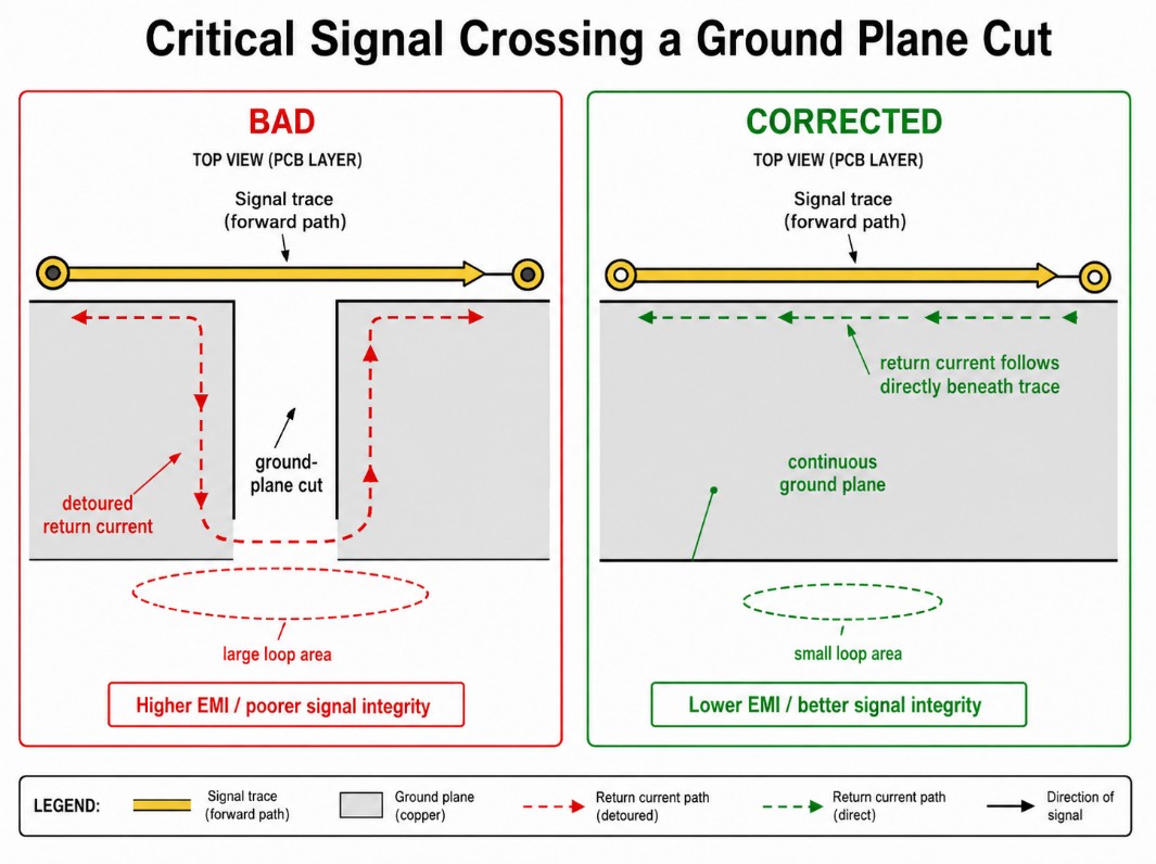
Critical signal crossing a ground plane cut.
Texas Instruments High-Speed Interface Layout Guidelines recommends routing high-speed signals over a solid ground reference rather than across plane splits or voids. The guide notes that crossing an opening forces high-frequency return current to take a longer route, which can increase emissions and degrade signal integrity.
Insufficient Copper Pour Coverage
A copper pour can cover a large part of the board and still contain weak current paths. The problem usually appears where clearances around pads, vias, mounting holes, or routed traces leave only a narrow strip of copper connecting two larger regions.
That narrow section may carry the current for an entire circuit block. As current increases, the resistance of the restriction causes additional voltage drop and heat. The rest of the plane may remain cool, which makes the local bottleneck difficult to notice during a basic visual review.
Pay particular attention to regulator outputs, power connectors, motor drivers, high-current loads, and bulk capacitors. Zoom in around these areas after rebuilding the copper pour. Check whether several nearby clearances combine to create a thin path or divide the copper into isolated islands.
Thermal-relief connections also need to match the expected current. They make soldering easier, but very narrow spokes can restrict current into connectors, power components, or large pads. High-current connections may require wider spokes or direct copper connections, depending on assembly needs and thermal behaviour.
The current-carrying capability of a conductor depends on more than its visible width. Copper thickness, temperature rise, board construction, nearby copper, and operating conditions all matter. IPC-2152 provides guidance for evaluating current capacity and conductor temperature rise.
Before ordering, inspect the Gerber files rather than relying only on the PCB editor. Confirm that every important power region is present, connected to the correct net, and free from unexpected clearances or isolated copper sections. The selected copper weight and fabrication options should also be checked against JLCPCB's ordering requirements.
Ignoring Plane Impedance at High Frequencies
At low frequencies, a power or ground plane may appear to behave like a simple low-resistance conductor. At higher frequencies, inductance, capacitance, dielectric spacing, and the physical relationship between the planes become increasingly important.
A fast signal does not interact only with the visible trace. Its behaviour also depends on the nearby reference plane. Changing the distance between the trace and plane changes the impedance, even when the trace width remains the same. Plane gaps, voids, and layer transitions can introduce additional discontinuities.
Power and ground planes placed close together also form distributed capacitance. This can support the local decoupling network, but it does not remove the need for correctly placed capacitors. Plane capacitance and discrete capacitors work together across different frequency ranges.
Generic impedance equations are useful during early design, but the final calculation should use the manufacturer's actual dielectric thickness, copper thickness, and stack-up. The JLCPCB PCB Impedance Calculator can be used to compare the selected board construction with the required trace geometry.
Controlled-impedance routes should remain over a continuous reference plane. When a signal changes layers, nearby ground vias should provide a short return transition. Any plane cut beneath the route can change the impedance and increase the chance of reflections, timing problems, or radiated noise.
FAQ about Circuit Board Ground Plane Design
Q: Does Every PCB Need a Ground Plane?
Not every simple PCB requires a dedicated plane layer, but most designs benefit from having a large and continuous ground area. A solid circuit board ground plane becomes increasingly important when the board contains fast digital signals, switching regulators, communication interfaces, or sensitive analog circuits. On a two-layer board, one side can often be kept mostly as ground while short signal routes are placed on the other side.
Q: Can a Two-Layer PCB Have an Effective Ground Plane?
Yes, although careful routing is required. Keep as much of one layer as possible available for ground copper and avoid cutting it into small sections with long traces. Ground stitching vias can connect top and bottom pours where necessary. After routing, inspect the plane for isolated islands, narrow connections, and gaps beneath important signals.
Q: Should Analog and Digital Grounds Always Be Separated?
No. Splitting the plane automatically can create longer return paths and cause signals to cross gaps. Many mixed-signal boards work better with one continuous ground plane and careful component placement. Analog and digital circuits should remain in their own physical areas so their return currents do not overlap. Follow the component manufacturer's grounding recommendation when a controlled split or single-point connection is required.
Q: How Many Ground Stitching Vias Should Be Used?
There is no fixed number that works for every board. Place stitching vias where they provide a useful connection, such as beside signal vias, around board edges, near connectors, and around shielded or noisy circuits. Via spacing depends on frequency, board size, stack-up, and EMI requirements. A smaller number of well-positioned vias is usually more useful than a large number placed without a clear purpose.
Q: Can Power and Ground Planes Be Placed Next to Each Other?
Yes. Keeping the power and ground planes close together reduces the inductance of the power-distribution path and creates distributed capacitance between the layers. This can support local decoupling, but it does not replace capacitors near IC power pins. The dielectric spacing and layer arrangement must match the manufacturer's stack-up.
Q: Should Unused Copper Areas Be Connected to Ground?
Usually, unused copper should either be intentionally connected to ground or removed. Floating copper islands can couple noise into nearby signals and may behave unpredictably at high frequencies. When unused copper is connected to ground, add suitable stitching vias and confirm that the copper does not create narrow clearances or interfere with controlled-impedance traces.
Conclusion about Circuit Board Ground Plane
A reliable circuit board ground plane is not simply unused copper connected to ground. It is part of the signal path, power-distribution network, EMI strategy, and thermal behaviour of the finished PCB. Decisions about plane continuity, layer order, return-current flow, and component placement should therefore be made before critical routing begins.
Solid reference planes are usually the safest choice for high-speed signals. Power regions should be checked for narrow copper necks, isolated islands, and weak connections around pads or vias. Decoupling capacitors need short connections to both the power pin and ground plane, while signal-layer changes should include a nearby path for return current.
Before manufacturing, rebuild all copper areas, run DRC, inspect the Gerber files, and compare the stack-up with JLCPCB's fabrication requirements. For boards with several power rails, mixed-signal sections, or controlled-impedance routing, the JLCPCB Layout Service can support placement and fabrication-aware PCB layout based on a completed schematic.
Keep Learning
Track Width v/s Current Capacity: PCB Layout Tips for Power Routing
Key Takeaways Trace width and copper thickness set the current limit. Standard 1 oz (35 µm) copper suits most designs; step up to 2–3 oz for power-hungry boards. Size traces against IPC-2221/IPC-2152 for a safe temperature rise. Internal layers carry less current than external ones. Buried traces dissipate heat poorly, so derate them or move high-current paths to outer layers. Vias are a bottleneck—each carries only about 500 mA. When routing power across layers, stitch multiple vias in parallel rathe......
Circuit Board Ground Plane and Power Plane Guide 2026
Key Takeaways Continuous copper first: A solid circuit board ground plane creates a low-impedance return path, reduces noise, and is usually safer than split planes, even on mixed-signal boards. Think in current loops: Every signal needs a return path directly beneath it. Never route high-speed traces across plane gaps, slots, or cutouts. Plan the stack-up early: Choose the layer arrangement before routing critical signals, and keep power and ground planes close together to lower distribution inductan......
Guide to Ground Bounce in PCB - Causes, Effects & Prevention
Key Takeaways Ground bounce is a voltage spike between an IC's die ground and the PCB ground. It happens when current changes fast through parasitic inductance (V = L x di/dt). Many outputs switching at once, called SSO, make it much worse. It can cause logic errors, false resets, and ringing on signals. You measure it with a quiet-low sense line on a scope. Good decoupling, short ground loops, and slower slew rates fix most of it. Introduction A board passes every test on the bench. Then, in the fiel......
Voltage Regulator PCB: Practical Design Guide
Key Takeaways A voltage regulator PCB doesn't just convert one voltage into another; it must also provide a stable output while handling heat, load changes, and noise in the circuit. The layout is as important as the regulator IC; keep the input and output capacitors near the pins, use short power connections, and ensure a direct, low-impedance ground return. Linear regulators are simple and quiet, but they lose voltage difference as heat; switching regulators are the better option when the voltage dr......
LDO vs Switching Regulator: Comparison & PCB Layout
Key Takeaways Calculate LDO dissipation first: Always calculate LDO power dissipation at maximum input voltage and load before comparing packages or prices. Condition-dependent specs: Treat dropout, PSRR, noise, ripple, efficiency, and transient response as condition-dependent, not fixed values. Layout matters for both: A buck converter's high-di/dt input loop and high-dv/dt switch node create different coupling mechanisms. Both need deliberate PCB placement. Output capacitor selection: The output cap......
Understanding Star Grounding in PCB Design: A Practical Guide
Key Takeaways Controlled Return Paths: Star grounding gives selected circuit blocks separate return paths that meet at one controlled physical point. It limits shared-impedance coupling between noisy and sensitive sections. Best Applications: It works best in compact, low-frequency, low-current, or noise-sensitive systems, including audio stages, sensor interfaces, and selected precision circuits. Ground Plane Alternative: A ground plane provides a broad, low-inductance reference that is normally bett......