
How to Reduce Noise and EMI in PCB Layout: A Comprehensive Design Guide
12 min
- EMI in PCB Design: Why EMI and Noise Occur in PCB Layouts?
- PCB Design Guidelines for Reduced EMI Through Layout Optimization
- EMI PCB Layout Design: Component Placement Strategies
- Routing Techniques for Low-Noise PCB Board Layout
- Grounding and Power Strategy in EMI PCB Design
- Advanced Techniques for Reducing EMI in PCB Layout Design
- FAQ about How to Reduce Noise and EMI in PCB Layout
Key Takeaways
EMI origins: EMI stems from structural layout deficiencies — poor return paths, interrupted reference planes, and large loop areas create antenna structures that radiate unwanted energy.
Loop area is critical: Minimizing current loop areas through solid ground planes adjacent to signal layers is the single most effective EMI reduction technique.
Placement defines noise: Component placement establishes current loops before routing. Group by function (power, analog, digital, RF), isolate analog from digital sections, and keep noise sources away from sensitive circuits.
Grounding & power integrity: A continuous ground plane, optimized PDN with tight power-ground spacing, and correctly placed decoupling capacitors form the foundation of low-noise design.
Advanced suppression: Shielding (λ/20 aperture rule), filtering (ferrite beads, common-mode chokes), and gate-drive control with RC snubbers provide additional EMI suppression for demanding applications.
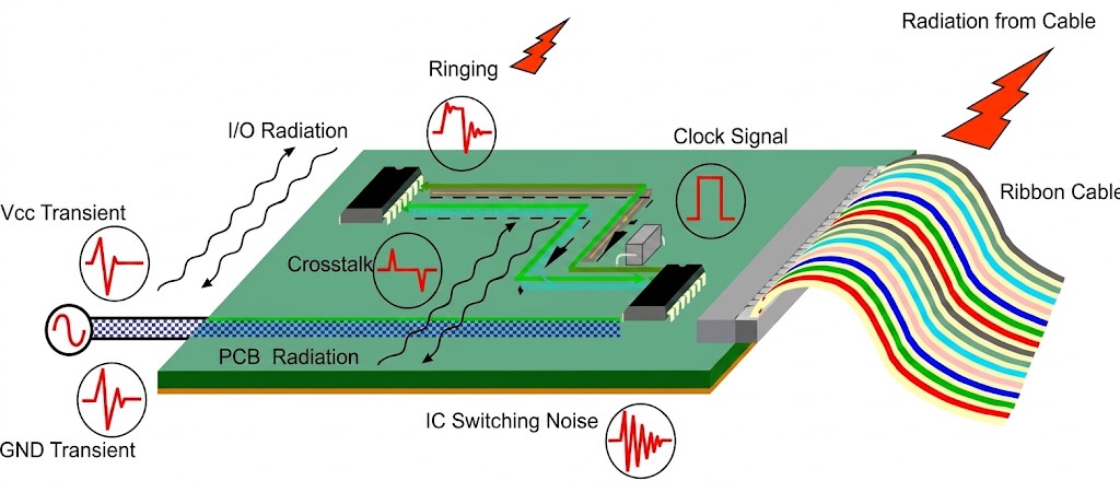
Electronic design is often a battle against invisible forces. You may have a perfect schematic, but the physical implementation of a circuit board introduces complex electromagnetic interference (EMI).
In professional manufacturing, EMI is the cause, and noise is the result. EMI is the propagation of unwanted energy. Noise is the manifestation of that energy as signal distortion or jitter. Most system noise stems from improper layout decisions made during the initial design phase. This makes the PCB layout your primary line of defense.
That's when knowing how to reduce noise and EMI in PCB layout becomes a significant part. In this guide, we take you through systematic methods in PCB design and layout optimization that help you handle EMI and Noise.
EMI in PCB Design: Why EMI and Noise Occur in PCB Layouts?
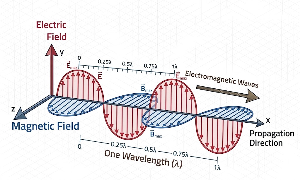
The occurrence of EMI and noise is rooted in the physics of electric and magnetic fields. EMI arises when fields surrounding conductors interact with unintended parts of the system. At high frequencies, every trace on a PCB must be viewed as an antenna. These traces can both radiate and receive energy.
The goal of a low-noise design is field confinement. You must contain these fields within specific dielectric volumes.
The Relationship Between EMI Sources and Noise Manifestation
Noise is rarely a random occurrence. It typically stems from structural layout deficiencies that allow fields to couple into victim circuits. EMI sources are classified as conducted or radiated.
Conducted EMI travels through physical paths like power rails. Radiated EMI propagates through air or dielectric as waves. Radiation happens when charges undergo acceleration. This occurs during digital switching or high-frequency power conversion.
If these charges are not canceled by an equal and opposite charge nearby, a net field is established. This follows the Ampere-Maxwell law. It relates magnetic fields to current density. Faraday's law also applies here. It relates electric fields to time-varying magnetic fields.
Common Root Causes in Circuit Board Layout
The most frequent causes of EMI in circuit board layouts are as follows:
- Return Current Path Mismanagement: This is the most frequent cause of EMI. Designers often focus exclusively on the signal trace while neglecting the fact that current must always flow in a closed loop.
- Neglecting AC Impedance: In high-speed systems, return current does not follow the path of least resistance (DC); instead, it follows the path of least loop inductance (lowest AC impedance).
- Interrupted Reference Planes: The ideal return path is located directly beneath the signal trace on an adjacent plane. When this plane is interrupted by splits, slots, or cutouts, the return current is forced to take a long detour.
- Large Loop Areas: Detoured return paths create significant loop areas between the "send" and "return" signals. These loops function as magnetic dipole antennas, efficiently radiating and receiving interference.
- Poor Grounding Strategies: Weak grounding allows common-mode noise to circulate throughout the system.
- Cable Radiation: Uncontrolled common-mode noise often escapes the board through connected cables, which act as the dominant radiators in systems that fail emissions testing.
PCB Design Guidelines for Reduced EMI Through Layout Optimization
Systemic EMI control is a holistic structural design challenge. Effective reduction focuses on the geometric relationship between current paths. By minimizing the volume where fields reside, you reduce radiation risks. Here's how to reduce EMI:
Minimize Current Loop Area
Reducing the current loop area is the most critical principle. The strength of radiated emissions from a loop is proportional to its area. It also depends on the signal current and the square of the frequency.
For a 500 MHz circuit, a small reduction in loop area drastically decreases the EMI signature. The most effective method is using a solid, continuous ground plane. Place it immediately adjacent to the signal layer.
Avoid Irregular Shapes
The physical shape of a PCB impacts its electromagnetic behavior. Compact, rectangular shapes are superior to irregular designs. Irregular shapes force signals to take indirect paths. This increases parasitic inductance. In high-frequency applications, traces longer than one-tenth of the wavelength are transmission lines.
For a 1 GHz signal, this is roughly 1.4 cm on FR4. Keep traces short in compact layouts. Avoid sharp corners on the board edge. They become points of high electric field intensity. Use rounded corners with a radius of at least 1 mm.
Control Trace Length and Routing Paths
High-speed signals must follow the shortest and most direct paths. Every extra millimeter of trace length adds parasitic inductance. This leads to voltage spikes based on:
$V = L \cdot \frac{dI}{dt}$
Route critical signals like clocks on internal layers. Use a stripline structure between ground planes. This configuration provides superior field containment. It is much better than outer-layer microstrip routing. Keep traces at least 20 mils from the board edge to prevent field fringing.
EMI PCB Layout Design: Component Placement Strategies
Component placement is more critical than routing because it defines the initial current loops and physical separation. If placement is poor, even clever routing cannot fully resolve the resulting EMI in PCB design issues.
Group Components Based on Signal Flow
Apply functional zoning by dividing the board into power, analog, digital, and RF sections. Grouping components within these zones minimizes trace lengths and contains interference.
High-speed connectors should stay near their processing chips to reduce signal exposure. Position I/O circuitry at the board edge to create a clean boundary and prevent noise from leaking into cable harnesses.
Separate Analog and Digital Sections
Physically isolate digital circuits from sensitive analog paths to prevent switching noise coupling. In complex designs, use dedicated ground planes joined only at a single point to prevent shared return paths.
When signals must cross zones, never route them over a split in the ground plane. This detours return current and creates a loop antenna. Instead, route signals over a copper bridge to ensure a controlled return path.
Keep Noise Sources Away from Sensitive Circuits
Keep high-voltage and switching elements, such as regulators and transformers, out of harm's way of sensitive sensors.
A separation of 1 to 2 inches should be targeted in high-frequency sources. In high-density layouts, optimization of professional placements can be used to compromise thermal needs and electrical noise reduction.
Strategic placement is the foundation of a reliable board. When dealing with high-complexity designs, you should look forward to professional layout services to test your design to all EMI requirements.
Routing Techniques for Low-Noise PCB Board Layout
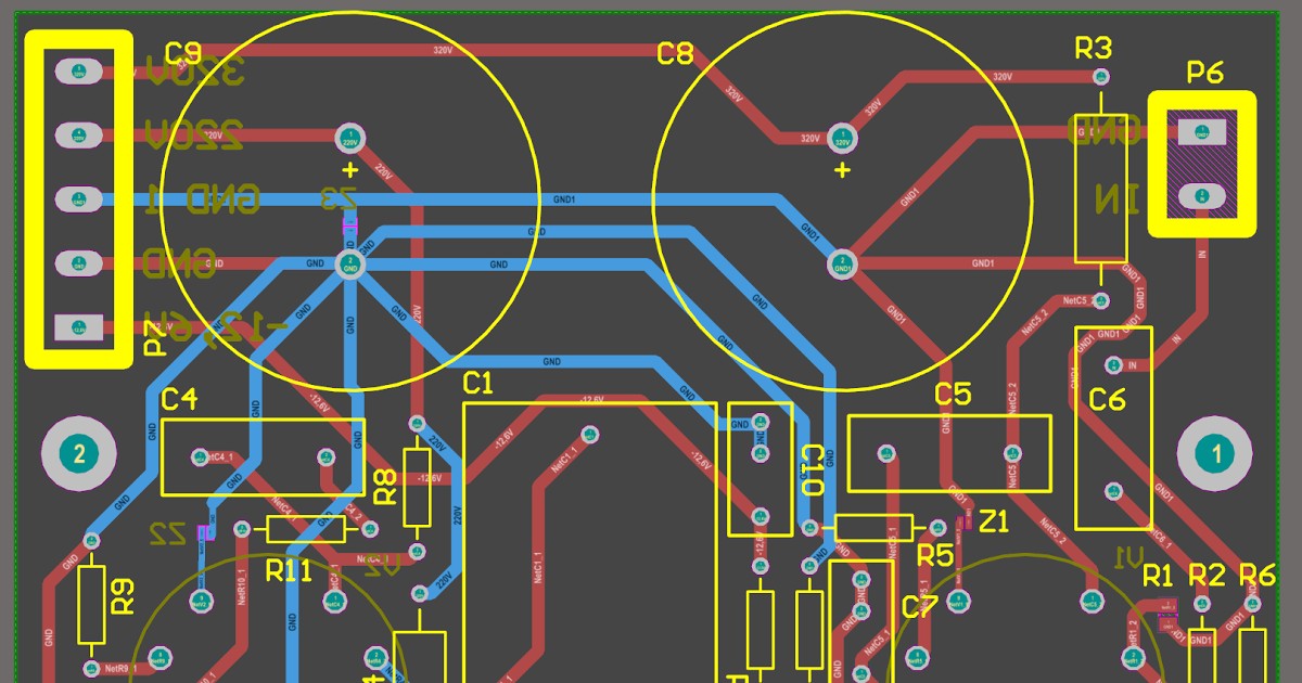
Effective routing implements the current loops established during placement. High-speed signals require consistent impedance and a continuous, low-inductance return path to prevent interference. Here's how the routing should look in EMI PCB layout design:
Maintain Continuous Return Current Paths
At high frequencies, current follows the path of least inductance directly beneath the signal trace. Any discontinuity in the reference plane, such as a split or gap, forces the current to detour. This increases the loop area and radiation.
When signals change layers, place stitching vias near the signal via to connect the reference planes. This provides a vertical path for return current, maintains field confinement, and prevents common-mode radiation.
Apply Proper Trace Spacing to Reduce Crosstalk
Manage crosstalk by increasing separation between parallel lines. Follow the "3W Rule" spacing traces at three times their width to reduce electromagnetic coupling by up to 70%.
Use 4W or 5W spacing for sensitive lines like clocks. In high-density layouts, use grounded guard traces between critical signals to absorb electric fields and provide isolation.
Route High-Speed Signals with Care
Differential signaling provides noise immunity by canceling far-field radiation. However, pairs must be perfectly length-matched. Any skew converts the signal to common-mode noise, leading to radiation and signal loss.
Limit the number of vias on high-speed lines to ensure that the inductance of the vias is reduced. Where vias are needed, match them to the trace impedance and blind or buried vias so as to remove stubs, which become resonant antennas at high frequencies.
Grounding and Power Strategy in EMI PCB Design
The power distribution network (PDN) is the foundation of EMI control. A stable PDN provides a consistent energy reservoir, preventing the generation of power-related noise and system instability. The strategy you can follow in EMI PCB design is as follows:
Use a Solid Ground Plane for Noise Reduction
A continuous ground plane is the most effective tool for managing EMI. It provides a low-impedance reference and contains electromagnetic fields. At frequencies more than 1 MHz, single-point grounding does not work; multi-point grounding to a solid plane is the strategy of choice.
In multilayer stackups, ensure that the ground plane is as close to the signal layers as possible. A slimmer dielectric makes a better confinement of fields. The 4-layer stackup, which is the standard stackup, consists of Signal-GND-Power-Signal, where each signal layer has an adjacent reference plane.
Optimize Power Distribution to Reduce Noise
Maintaining low PDN impedance across a wide frequency range is critical. High impedance causes voltage fluctuations during current draws.
To reduce the impedance, position power and ground planes as close as possible - preferably less than 10 mils. This gives a maximum inter-plane capacitance, which offers high-frequency decoupling incomparable to discrete capacitors.
Place Decoupling Capacitors Correctly
Decoupling capacitors act as local energy reservoirs to suppress power rail noise. Inductive parasitics between the loop and the IC power pins is minimized by placing them as close to the IC power pins as possible.
Having many capacitors with varying values deals with a wider frequency range; small capacitors deal with high-frequency transients, and larger capacitors deal with the stability of low frequencies. But beware of anti-resonance - a high-impedance peak which can arise where parallel capacitors with different values are in play.
Advanced Techniques for Reducing EMI in PCB Layout Design

In demanding applications, basic strategies may be insufficient. Advanced techniques provide extra layers of suppression. These include shielding and slew-rate control.
Apply Shielding and Filtering Methods
Shielding uses conductive materials to block electromagnetic waves. PCB-level shielding involves metal cans soldered over noisy sources. For a shield to be effective, apertures must be small. The "$\lambda/20$ Rule" is the standard. The longest dimension of any opening must be less than one-twentieth of the wavelength.
Filtering removes unwanted noise from the signal and power lines. Ferrite beads and common-mode chokes are essential. They provide conducted EMI filtering on the I/O ports. Common-mode chokes are effective on differential data lines, such as USB. They block noise without distorting the high-speed signal.
Control Switching Behavior in Power Circuits
Switch-mode power supplies are notorious EMI sources. They have high dV/dt and dI/dt values. One advanced method is controlling the gate drive of power transistors. Increasing gate resistance slows down switching edges. This reduces high-frequency harmonics that drive emissions. Slower switching increases power dissipation.
To achieve balance, use RC snubber circuits. Place them across a power switch to absorb energy in parasitic inductances. This damps high-frequency ringing. Snubbers target parasitic resonance efficiently without slowing the entire transition.
Conclusion: How to Reduce Noise and EMI in PCB Layout
Low-EMI design is a pervasive architectural requirement. It is the result of synergy between layout structure, placement, and power management. You need to consider a PCB as a system of electromagnetic waveguides.
By following these principles, circuits are naturally silent and resistant. It takes a diagnostic attitude and professional best practices to succeed. Ensure that the invisible world of fields is managed with precision for reliability.
Optimize your next project for success. In complex designs, seeking professional services ensures your layout is of the highest technical standards.
FAQ about How to Reduce Noise and EMI in PCB Layout
Q: How do I manage EMI on a 2-layer board without a solid ground plane?
Control is more difficult on 2-layer boards. The primary strategy is routing every signal immediately adjacent to its return trace. This minimizes the loop area.
Q: Should I use a common-mode choke on every differential pair?
Not necessarily. Use them on cables leaving the enclosure or if the board fails radiated tests. For internal pairs, a well-matched layout is usually enough.
Q: Why does my switching regulator fail tests above 30 MHz?
This is often caused by parasitic capacitance in the layout. It allows noise to bypass the inductor or common-mode choke.
Q: How far should high-speed traces be from the board edge?
Keep them at least one dielectric thickness away from the edge. This prevents field fringing. The "20H Rule" is a common industry standard.
Q: Does via stitching really reduce radiated noise?
Yes. It creates a vertical path for return currents. This prevents common-mode noise from spreading across the board.
Keep Learning
BGA PCB Design Complete Guide: Layout and Routing Guidelines
Key Takeaways Define pad type first: Always confirm SMD or NSMD pad strategy before routing BGA fanout. NSMD is generally preferred for better solder joint formation, while SMD suits very small pads or tight mask registration. Match the process to the pitch: 0.8 mm BGAs work with dog-bone fanout and standard vias; 0.5 mm BGAs typically need via-in-pad or HDI routing. Picking the right via strategy early saves layers and cost. Place decoupling capacitors on the bottom side: Mount MLCCs directly under t......
PCB Design Rules and Guidelines: A Complete Best Practices Guide
A great schematic is just an idea. To turn it into a real, working product, you need to follow a robust set of Printed Circuit Board Design Rules. Ignoring these rules leads to costly respins, signal integrity (SI) failures, and boards that are physically impossible to build. This guide is a technical resource for the entire design process. We'll cover the essential rules for schematics, layout, and manufacturing that every engineer and hobbyist needs to know for a successful design. What Are PCB Desi......
Mastering PCB Design: A Step-by-Step PCB Layout Process Guide
Key Takeaways Process over improvisation: A repeatable, standardized PCB layout process—not luck—is what turns a working schematic into a board that succeeds on the first spin. Placement drives everything: Component layout and functional block partitioning are the most impactful steps; good placement makes routing easy, poor placement makes it impossible. Route critical signals manually first: Clocks, differential pairs, sensitive analog nets, and power switching loops must be hand-routed before auto-......
Multilayer PCB Design Guidelines: Stack-up and Layout Best Practices
Key Takeaways Stack-up is the foundation: The layer arrangement defines signal integrity, impedance control, and EMI performance — plan it before routing a single trace. Symmetric, reference-heavy designs prevent failures: A balanced stack-up with ground planes adjacent to every signal layer avoids warpage, ensures return path continuity, and minimizes crosstalk. DFM rules ensure manufacturability: Aspect ratio, annular rings, material selection, and symmetric copper distribution are critical to produ......
How to Reduce Noise and EMI in PCB Layout: A Comprehensive Design Guide
Key Takeaways EMI origins: EMI stems from structural layout deficiencies — poor return paths, interrupted reference planes, and large loop areas create antenna structures that radiate unwanted energy. Loop area is critical: Minimizing current loop areas through solid ground planes adjacent to signal layers is the single most effective EMI reduction technique. Placement defines noise: Component placement establishes current loops before routing. Group by function (power, analog, digital, RF), isolate a......
What is the Difference Between PCB Design and Layout?
The difference between PCB design and PCB layout trips up more engineers than you’d expect. While often used interchangeably, these are distinct disciplines. The gap between them is where many projects quietly go sideways. Simply put, PCB design is the logical foundation, while PCB layout is the physical implementation. A flawless schematic can fail in production due to poor layout, and even the best layout engineer can’t rescue it. Below, we provide a detailed breakdown of the differences between the......