
What is the Difference Between PCB Design and Layout?
12 min
- What Is PCB Design?
- What Is Printed Circuit Layout?
- PCB Design vs. PCB Layout: Major differences
- Core Processes in PCB Design and Layout
- Why Both PCB Design and PCB Board Layout Matter?
- Best Practices for Effective PCB Development
- Frequently Asked Questions about PCB Design and Layout
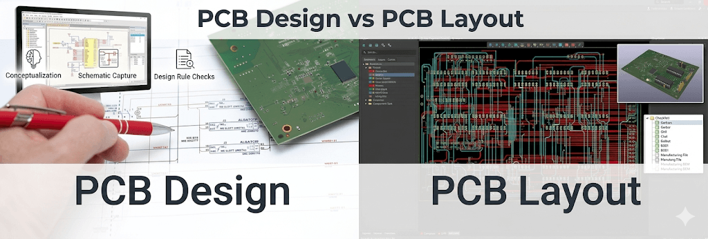
The difference between PCB design and PCB layout trips up more engineers than you’d expect. While often used interchangeably, these are distinct disciplines. The gap between them is where many projects quietly go sideways.
Simply put, PCB design is the logical foundation, while PCB layout is the physical implementation. A flawless schematic can fail in production due to poor layout, and even the best layout engineer can’t rescue it.
Below, we provide a detailed breakdown of the differences between the two so you can better understand how they work.
What Is PCB Design?
PCB design is the architectural phase of development. It’s where abstract electrical theory is translated into a logical blueprint. Before any physical trace is routed, this stage establishes the "soul" of the device, focusing entirely on circuit logic and electrical integrity.
In professional engineering, "design" refers to the conceptualization and validation of the circuit. Its scope includes:
- Circuit Theory: Calculating component values to meet performance targets.
- BOM Management: Sourcing parts based on specs, budget, and availability.
- Schematic Capture: Digitizing the circuit using symbols to represent electrical relationships.
- ERC (Electrical Rules Check): Identifying logical errors, like conflicting voltage rails, before they reach the physical board.
The Role in Product Development
PCB design is the master contract of the R&D lifecycle. The choice of microcontroller or communication protocols, which are decisions here, determines the mechanical housing, thermal profiles, and overall manufacturing cost. Even the best layout will not help the product if the design is faulty.
The journey from a concept to a physical board follows a structured path:
- Functional Requirements: This defines what the device should do.
- Block Diagramming: Subsystems of requirements are broken down (Power, Logic, I/O).
- Schematic Capture: A network of component symbols linked together by logical wires or nets.
- Netlist Generation: Creating the machine-readable "map" that tells layout software which physical pads must be joined by copper.
Why Accurate Planning Is Critical
The diagnostic reality is that foundational errors aren't fixed downstream. Rushing circuit planning is a leading cause of project failure. An error in the schematic, such as a swapped TX/RX pair, is invisible to the layout tool’s physical checks.
Precision here prevents "spinning" a board (re-manufacturing) simply because the logic was never sound. Accurate design ensures you are building on a verified, stable foundation.
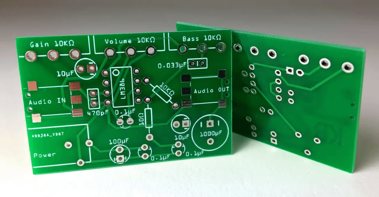
What Is Printed Circuit Layout?
PCB layout is the physical implementation of the design contract. If design is the "soul" of the device, the layout is its "body," it is where abstract electrical logic meets real-world physics, geometry, and manufacturing constraints.
In the printed circuit layout phase, the focus shifts from what is connected to where and how those connections physically exist. Its scope includes:
- Spatial Engineering: Positioning components within the 3D constraints of a mechanical enclosure.
- Trace Geometry: Defining copper widths and spacing to handle specific current loads and impedance requirements.
- Thermal Architecture: The thermal architecture is the design of thermal paths, thermal vias, and copper pours to maintain components at safe operating temperatures.
- Manufacturing Compliance: Making sure that the design is within the physical constraints of the fabrication house.
Translating Schematic to Physical Form
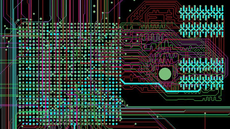
The transition begins with the netlist, the machine-readable "map" generated during the design phase. The layout engineer imports this data into a physical environment defined by the board stack-up.
Choosing the number of layers is the first major physical decision, as it dictates the available "real estate" for routing and the quality of the ground planes used for noise suppression.
Strategic placement is arguably the most critical skill in PCB board layout.
- Placement Strategy: The elements are placed in a manner that reduces the length of signal paths and separates high-speed digital logic devices and the sensitive analog sensors. Good placement: routing is easy; bad placement: routing is impossible.
- Precision Routing: After locking up parts, copper traces are routed to connect them. Low-speed signals are easy, but the high-speed interface is challenging because manual accuracy is needed to control signal integrity, making sure data pulses do not degrade or cause crosstalk with adjacent traces (crosstalk).
Manufacturing Constraints and DFM
The layout phase concludes with the Design for Manufacturability (DFM) phase. All physical characteristics, via, trace, and solder pad should be within tolerances of the fabrication house. Clearance should be observed to avoid short-circuiting, and solder mask holes should be accurate to achieve quality assembly.
The resulting product is a collection of Gerber or ODB++ files, which give the factory the precise coordinates to use to create the physical board.
Upload your design and get a fast quote for your next PCB layout online.
PCB Design vs. PCB Layout: Major differences
Get a quick look at the key differences between PCB Design and PCB Layout for a better understanding.
| Dimension | PCB Design (Logic) | PCB Layout (Physical) |
|---|---|---|
| Definition | Logical planning of connections | Physical placement and routing |
| Main Objective | Circuit functionality | Reliability and manufacturability |
| Key Tasks | Schematic capture, component selection | Stack-up design, routing, DRC |
| Tools Used | KiCad, Altium Schematic, OrCAD | Altium PCB, Allegro, PADS |
| Input | Requirements, datasheets | Netlist, board dimensions, BOM |
| Output | Schematic, netlist, BOM | Gerber files, drill files |
| Design Focus | Electrical logic | Signal integrity, Thermals, DFM |
| Expertise | Electrical Engineering (EE) | PCB Designer / CAD Specialist |
| Impact | Does it work logically? | Can it be built and stay cool? |
Core Processes in PCB Design and Layout
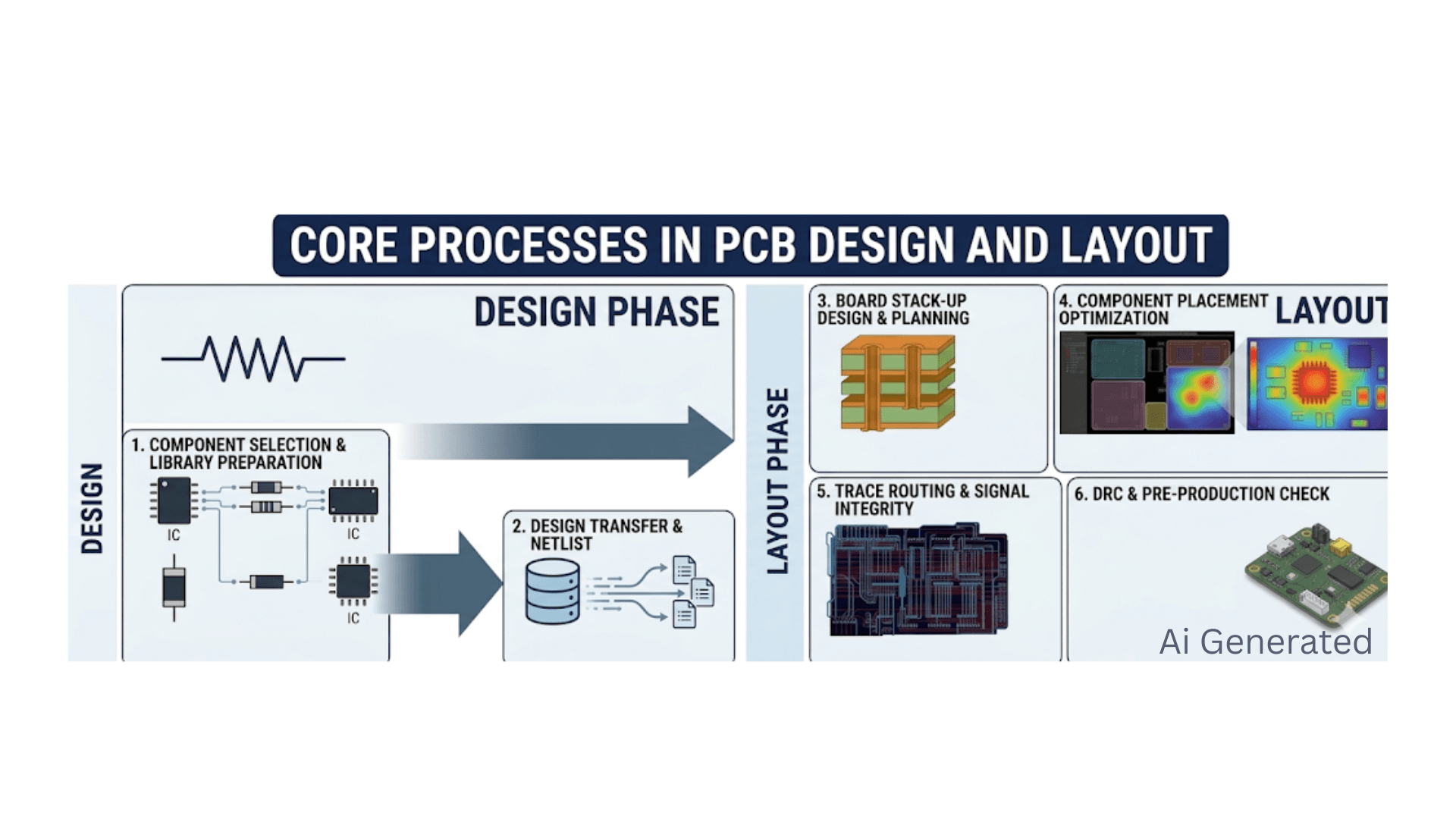
The process of bringing an idea of a concept to a manufactured board is a meticulous process. In this section, the fundamental stages that will be used to fill in the gap between logical design and physical implementation will be disaggregated.
Schematic Capture and Circuit Design Process
The lifecycle starts with schematic capture, wherein the electrical engineer specifies the logic of the circuit with standardized symbols. The latter is aimed at the proper connection of the electrical: determining the name of the net, and values assigned to the components, in order to have the device fulfill the purpose it is meant to serve.
Component Selection and Library Preparation
The key to success in the development is picking the appropriate components and creating proper library parts. This includes not only ensuring electrical specifications but also ensuring that each component has a proven schematic symbol and an accurate PCB board layout footprint that matches the actual physical package.
PCB Layout Planning and Board Stack-Up Design
The physical layout of the board has to be specified first, with the help of a stack-up design, before commencing the routing. This includes selecting the number of layers and the dielectric materials to be used, which will give the required signal isolation and power distribution.
Component Placement Optimization Strategy
The stage of placement is probably the most leveraged step of the layout process. Components are carefully placed by engineers so as to reduce signal path length, thermal hotspots, and isolate sensitive analog signals and noisy digital logic.
Trace Routing and Signal Integrity Considerations
Routing involves connecting component pads and copper traces according to the netlist. In the case of high-speed signals, it necessitates an in-depth knowledge of signal integrity, including matching length, routing, and differential pair routing, as well as path continuity.
Design Rule Check (DRC) and Pre-Production Check.
A stringent verification process with Design Rule Checks (DRC) is the last step prior to manufacturing. This scan is automated to verify that all the physical geometries, like trace widths, clearances, and via sizes, are within the fabrication house's capabilities.
Why Both PCB Design and PCB Board Layout Matter?
Design and layout are two sides of the same coin, although they are two different stages. Their effective integration is what makes the difference in the performance, reliability, and cost-effectiveness of the electronic assembly that is going to be made ultimately.
Ensuring Signal Integrity through Schematic Precision
The design phase determines the maximum performance of the whole product in terms of the choice of the components and ICs. The theoretical capability of the device is defined by the decisions made during the schematic capture, like which high-speed transceivers to use, or what voltage reference to use, etc.
Without the original design taking into consideration the signal conditioning required, it is impossible to regain the lost performance with all the optimization of the layout.
Establishing a Stable Foundation for Power Distribution
A robust electrical design is a starting point for a stable power delivery network (PDN). The designer of the circuit can achieve this by specifying suitable decoupling techniques and voltage rail considerations in the schematic to make sure that the circuit will possess the required "reservoirs" of energy to manage switching transients.
It is this logical planning that enables the layout stage to effectively put into practice low-impedance power paths that avoid system resets or corruption of data.
Mitigating Thermal Risks via Strategic Layout
Although the design determines which components will produce heat, the location where the heat goes is determined by the layout of the printed circuit. Thermal vias, copper pours, and component placement in strategic locations are some of the techniques employed by layout engineers to remove heat from sensitive regions and channel it to heat sinks or the board surface.
The result of such physical management is that a logically ideal circuit may be thermally throttled or experience an early component failure without this physical management.
Manufacturing with DFM-Focused Layouts
The quality of layout is the main factor of success in manufacturing and its long-term durability. Design for Manufacturability (DFM) rules used in the layout stage help to avoid typical assembly errors like solder bridging and tombstoning of small parts.
The layout, which is conscious of manufacturing tolerances, would guarantee a high first-pass yield, directly decreasing production costs and enhancing the uniformity of the end product.
Synergy Between Design and Layout
The most successful products are due to the continuous communication between the design and layout processes. Collaboration between engineers can help define the possible physical constraints at an early stage.
This synergy will avoid the throw it over the wall attitude that will most likely result in several design cycles and slow product development.
Best Practices for Effective PCB Development
To have high-quality boards the first time round, the best method is to be systematic in the approach to development. These best practices give a guideline on how to keep the coordination and technical excellence at all levels.
Define Clear Requirements Before Starting Design
Each project must commence with a clear specification, which has electrical, mechanical, and thermal constraints. Both demand locking such requirements prior to opening an ECAD tool, which helps in avoiding scope creep and minimizes the occurrence of disruptive changes towards the end of the cycle.
Optimize Component Placement for Better Signal Flow
Consider physical implementation as the most crucial part of the process. Combine all the related components, like decoupling capacitors, as close to the power pins as possible, to make current loops small.
Pay Attention to Routing, Power, and Ground Design
Ensure that a good ground plane strategy is adopted to ensure that all the signals have a low-impedance return path. When routing, make sure that the traces of power are wide enough to support the amount of current needed, without the excess heat or voltage drop.
Follow DFM Rules and Perform Design Rule Checks
Design for manufacturability (DFM) guidelines should be considered in your workflow since the very first step of the layout is the layout stage. It is a small fix to find a violation of clearances in the middle of routing, but it can cause hours of rework to find the violation when it is found in a final review.
Ensure Close Collaboration Between Design and Layout Teams
Have constant feedback between the schematic and the board layout. To make certain that any physical modifications performed during layout, like interchanging pins in order to ease routing, are automatically updated in the schematic logic, use back-annotation.
Need reliable PCB layout services? Avoid expensive design iterations and ensure your project is production-ready.
Hurry and grab this limited-time discount!
At the end of the day, PCB design and layout are two halves of a single, high-stakes conversation. While the design phase defines the circuit’s logical "soul," the layout builds the physical "body" that must survive real-world physics and manufacturing.
A perfect schematic is just a theory until a skilled layout makes it a reality, and as many engineers have learned the hard way, a "flawless" design can still fail at the finish line if signal integrity or thermal management is ignored.
By bridging the gap between electrical logic and physical implementation with precision, you don’t just build a board; you ensure a high-yield, reliable product that is ready for the long haul.
Frequently Asked Questions about PCB Design and Layout
Q: Can I skip the schematic and go straight to layout?
Not safely. The layout tool needs the netlist to verify connections. Skipping the schematic usually leads to "unconnected" nets and debugging nightmares.
Q: What is the difference between a PCB drawing and a PCB design drawing?
A PCB design drawing is the schematic (electrical intent). A PCB drawing refers to fabrication/assembly documents (physical dimensions).
Q: Does layout affect manufacturing cost?
Greatly. Layer count, via types (blind/buried), and trace density all drive the fabrication price. 3
Q: Why did my circuit pass simulation but fail EMI testing?
Simulation often checks logic, not physical parasitics. EMI issues like ground loops or antenna effects are created by the physical layout, not the schematic logic. 1
Q: What is back-annotation?
It’s the process of updating your schematic with changes made during layout (like pin swaps or reference designator updates) so both documents match.
Keep Learning
PCB Design Rules and Guidelines: A Complete Best Practices Guide
Key Takeaways Avoid Respins: Run early Schematic ERCs to stop design errors before layout begins. Protect SI/PI: Follow the 3W rule and never route high-speed traces over split ground planes. Match JLCPCB DFM: Set your DRC to JLCPCB capabilities (e.g., ≥ 3.5 mil trace/space, ≥ 0.15 mm vias). Use Free POFV: Utilize Via-in-Pad for dense boards—free on JLCPCB 6 to 20-layer stackups. Pre-Verify Designs: Use JLCPCB’s free online DFM and impedance tools to ensure first-time production success. A great schem......
BGA PCB Design Complete Guide: Layout and Routing Guidelines
Key Takeaways Define pad type first: Always confirm SMD or NSMD pad strategy before routing BGA fanout. NSMD is generally preferred for better solder joint formation, while SMD suits very small pads or tight mask registration. Match the process to the pitch: 0.8 mm BGAs work with dog-bone fanout and standard vias; 0.5 mm BGAs typically need via-in-pad or HDI routing. Picking the right via strategy early saves layers and cost. Place decoupling capacitors on the bottom side: Mount MLCCs directly under t......
Mastering PCB Design: A Step-by-Step PCB Layout Process Guide
Key Takeaways Process over improvisation: A repeatable, standardized PCB layout process—not luck—is what turns a working schematic into a board that succeeds on the first spin. Placement drives everything: Component layout and functional block partitioning are the most impactful steps; good placement makes routing easy, poor placement makes it impossible. Route critical signals manually first: Clocks, differential pairs, sensitive analog nets, and power switching loops must be hand-routed before auto-......
Multilayer PCB Design Guidelines: Stack-up and Layout Best Practices
Key Takeaways Stack-up is the foundation: The layer arrangement defines signal integrity, impedance control, and EMI performance — plan it before routing a single trace. Symmetric, reference-heavy designs prevent failures: A balanced stack-up with ground planes adjacent to every signal layer avoids warpage, ensures return path continuity, and minimizes crosstalk. DFM rules ensure manufacturability: Aspect ratio, annular rings, material selection, and symmetric copper distribution are critical to produ......
How to Reduce Noise and EMI in PCB Layout: A Comprehensive Design Guide
Key Takeaways EMI origins: EMI stems from structural layout deficiencies — poor return paths, interrupted reference planes, and large loop areas create antenna structures that radiate unwanted energy. Loop area is critical: Minimizing current loop areas through solid ground planes adjacent to signal layers is the single most effective EMI reduction technique. Placement defines noise: Component placement establishes current loops before routing. Group by function (power, analog, digital, RF), isolate a......
What is the Difference Between PCB Design and Layout?
The difference between PCB design and PCB layout trips up more engineers than you’d expect. While often used interchangeably, these are distinct disciplines. The gap between them is where many projects quietly go sideways. Simply put, PCB design is the logical foundation, while PCB layout is the physical implementation. A flawless schematic can fail in production due to poor layout, and even the best layout engineer can’t rescue it. Below, we provide a detailed breakdown of the differences between the......