
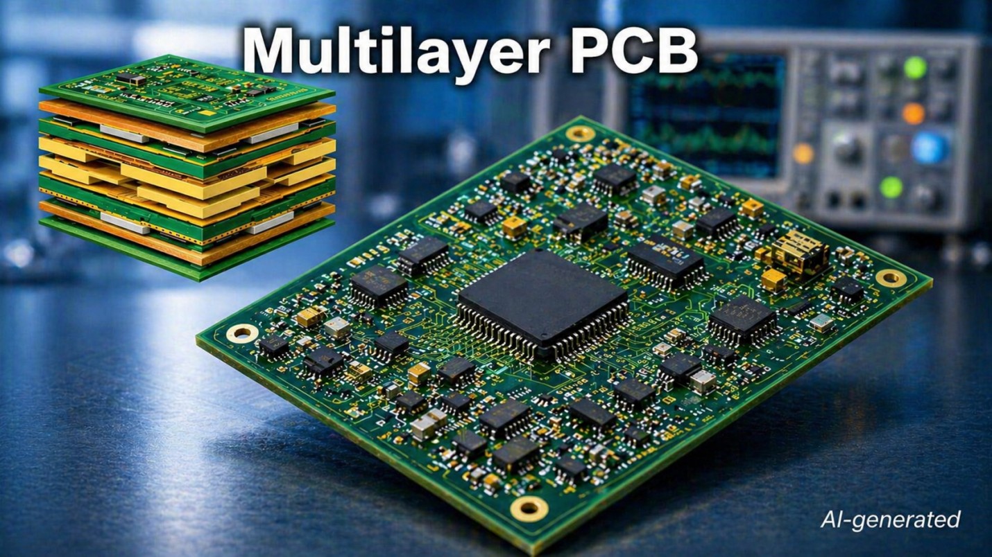
Multilayer PCB Design Guidelines: Stack-up and Layout Best Practices
13 min
- Common Challenges in Multilayer PCB Design: Why Complexity Fails?
- Multilayer PCB Stackup Design and Layer Planning
- Multilayer PCB Design Guidelines for Layout and Routing
- High-Speed and Multilayer RF PCB Design Considerations
- Via Design and Thermal Management in PCB Multilayer
- Manufacturing and DFM Guidelines for Multi-layer PCB Design
- FAQ about Multilayer PCB Design Guidelines
Key Takeaways
Stack-up is the foundation: The layer arrangement defines signal integrity, impedance control, and EMI performance — plan it before routing a single trace.
Symmetric, reference-heavy designs prevent failures: A balanced stack-up with ground planes adjacent to every signal layer avoids warpage, ensures return path continuity, and minimizes crosstalk.
DFM rules ensure manufacturability: Aspect ratio, annular rings, material selection, and symmetric copper distribution are critical to producing reliable boards at scale.
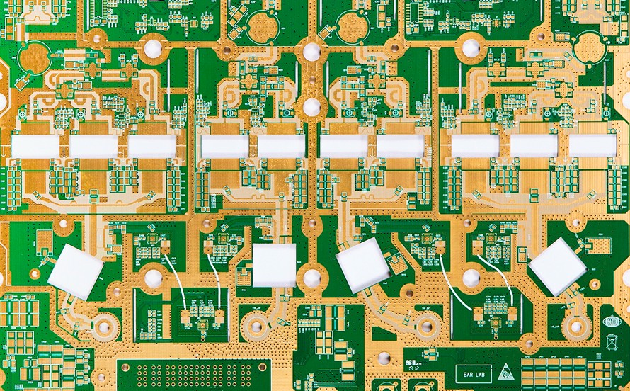
Modern electronics demand high functional density and extreme data rates. This evolution has transformed the printed circuit board from a passive carrier into a complex system element.
In high-performance environments, electromagnetic physics dictates every aspect of performance. The transition to a multilayer PCB design is no longer a choice but a necessity for systems using fast-switching logic or RF components.
Success depends on the physical arrangement of copper and dielectrics, the stack-up, which governs signal integrity and power stability.
Common Challenges in Multilayer PCB Design: Why Complexity Fails?
A multilayer PCB design architecture introduces failure modes that simpler boards avoid. These failures are rarely isolated. They are typically caused by multiple, interrelated design issues.
Problems with Signal Integrity and Crosstalk
At gigahertz frequencies, traces behave as transmission lines. Crosstalk occurs when electromagnetic coupling happens between adjacent traces. A victim trace picks up voltage or current from a neighboring aggressor.
This becomes harder to manage as routing density increases. Even low-frequency clocks can cause issues if they have sharp edge rates. Missing ground planes between signal layers can create broadside coupling, which is difficult to shield and often leads to timing failures.
Impedance Control Failures
Matching the impedance eliminates signal reflections, or ringing, and data loss. Impedance is a function of trace width, copper thickness, and the distance to the reference plane. Problems often occur when coordination with the fabricator is lacking.
If you use generic formulas without knowing the manufacturer specific materials, variations can exceed 10%. Resin flow during lamination can also shift dielectric thickness, altering the intended 50 Ω impedance.
Board Warpage from Asymmetric Stackup
Mechanical stability is as vital as electrical performance. Warpage, or bow and twist, happens when thermal expansion forces are unbalanced. This is usually caused by an asymmetric stack-up in which copper weight is not mirrored about the center axis.
During reflow at 230-250 ℃, materials expand at different rates. A heavy power plane on one side without a corresponding plane on the other will cause the board to bend. That can result in head-in-pillow issues on BGA packages.
What Separates a Good Design from a Failed One?
Good designs treat the PCB as a waveguide rather than a wire. It prioritizes propagation over simple connectivity.
| Design Attribute | Vulnerable Design | Robust Design |
|---|---|---|
| Return Path | Signals cross split planes | Continuous ground plane under every net |
| Stackup Symmetry | Random layer sequencing | Mirrored around the core |
| Impedance | Basic rules of thumb | Field solver simulations |
| Via Architecture | Excessive through-hole stubs | Strategic HDI and back-drilling |
| Thermal | Grouped heat sources | Distributed sources with thermal vias |
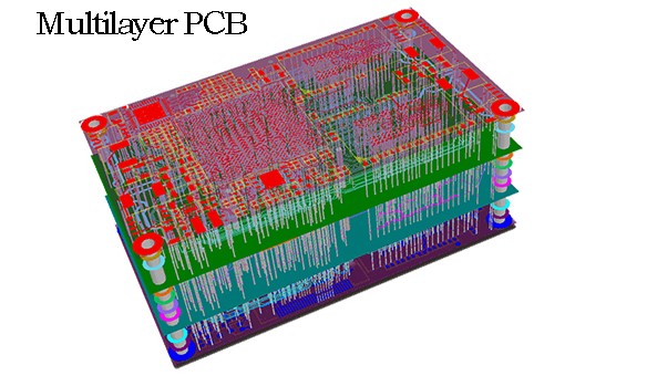
Multilayer PCB Stackup Design and Layer Planning
The stack-up is the foundation of your board. You must plan it before routing a single trace, as it dictates the electrical environment.
What is PCB Stackup?
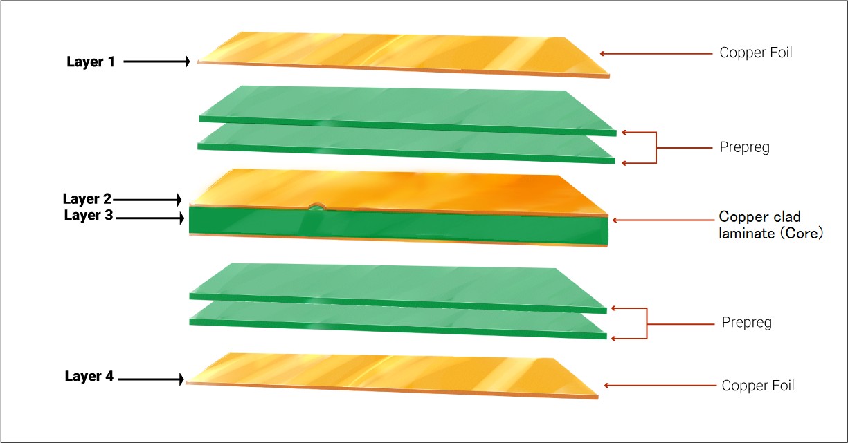
A multilayer PCB stackup is a sequence of copper foil, prepreg, and core layers. Cores are rigid laminate sheets with copper bonded to both sides. Prepreg is a semi-cured bonding agent. Under heat and pressure, these fuse into a single cohesive unit.
Layer Count and Configuration
Complexity and component density determine the number of layers. 4-layer PCBs work well for simple designs. But for complex designs with many dense BGAs (sub-0.65mm), 8, 16, or 32 layers may be required to provide sufficient routing layers and planes.
Signal, Power, and Ground Layer Arrangement
Proper layer arrangement mitigates noise. Follow these core principles:
Reference Plane Adjacency: Place high-speed layers next to solid ground planes.
Coupled Pairs: Power and ground planes must be kept close together (3 mils) to minimize interplane capacitance.
Orthogonal Routing: If two adjacent layers are used for signals, route one layer with horizontal signals and the other layer with vertical signals to avoid crosstalk.
Stackup for EMI and Signal Integrity
Effective EMI control uses the Faraday cage principle. Sandwiched high-speed signals between ground planes contain electromagnetic energy. For multi-gigahertz designs, use internal stripline layers rather than surface microstrip layers for improved shielding.
Standard Stackups for 4, 6, and 8-Layer PCBs
Using standard parameters ensures high precision and lower costs.
14-Layer Standard Stackup (1.6 mm)
The 4-layer configuration is the baseline for professional electronic design and cost-effective prototyping. This stackup uses a Signal-GND-Power-Signal arrangement. It ensures the primary signal layer has a dedicated ground reference to reduce EMI. This provides a stable balance of low manufacturing cost and reliable power distribution for standard embedded systems.
| Layer | Material | Thickness (mm) | Function |
|---|---|---|---|
| Top | Copper (1 oz) | 0.035 | Components and Critical Signals |
| L2 | Copper (0.5 oz) | 0.0152 | Continuous Ground Plane |
| Core | FR-4 | 1.065 | Structural Integrity |
| L3 | Copper (0.5 oz) | 0.0152 | Power Plane |
| Bottom | Copper (1 oz) | 0.035 | Routing |
Reference: JLCPCB JLC04161H-7628 Standard Stack-up
26-Layer Standard Stackup (1.6 mm)
The 6-layer configuration offers a significant improvement in routing density and signal isolation. This stackup uses a Signal-GND-Signal-Signal-Power-Signal arrangement. It introduces internal stripline layers that are inherently shielded from external electromagnetic noise. This provides superior signal integrity and is the ideal choice for designs with higher-speed digital interfaces.
| Layer | Material | Thickness (mm) | Function |
|---|---|---|---|
| Top | Copper (1 oz) | 0.035 | High-Speed Microstrip |
| L2 | Copper (0.5 oz) | 0.0152 | Ground Plane |
| L3 | Copper (0.5 oz) | 0.0152 | Internal Signal (Stripline) |
| L4 | Copper (0.5 oz) | 0.0152 | Internal Signal (Stripline) |
| L5 | Copper (0.5 oz) | 0.0152 | Power Plane |
| Bottom | Copper (1 oz) | 0.035 | Non-Critical Signals |
Reference: JLCPCB JLC06161H-3313 Standard Stack-up
38-Layer High-Performance Stackup (1.6 mm)
The 8-layer configuration is the gold standard for high-speed systems like PCIe Gen 4 or DDR4. This stackup uses a SIG-GND-SIG-PWR-GND-SIG-PWR-SIG arrangement. It ensures every signal layer is adjacent to a reference plane. This provides superior isolation and a low-impedance power distribution network (PDN).
| Layer | Material | Thickness (mm) | Function |
|---|---|---|---|
| Top | Copper (1 oz) | 0.035 | High-Speed Microstrip / Components |
| L2 | Copper (0.5 oz) | 0.0152 | Reference Ground Plane |
| L3 | Copper (0.5 oz) | 0.0152 | Internal Signal (Stripline) |
| L4 | Copper (0.5 oz) | 0.0152 | Primary Power Plane |
| L5 | Copper (0.5 oz) | 0.0152 | Shielding Ground Plane |
| L6 | Copper (0.5 oz) | 0.0152 | Internal Signal (Stripline) |
| L7 | Copper (0.5 oz) | 0.0152 | Secondary Power Plane |
| Bottom | Copper (1 oz) | 0.035 | Non-Critical Signals and Routing |
Reference: JLCPCB JLC08161H-3313 Standard Stack-up
Multilayer PCB Design Guidelines for Layout and Routing
The layout must execute the strategy defined by the stack-up.
Component Placement Best Practices
Placement dictates the physical limits of routing.
Functional Partitioning: Block functions (power, MCU, RF) to prevent digital interference on analog pins.
Decoupling Location: Place decoupling capacitors near IC power pins. Keep traces as short as possible to minimize inductance.
Thermal Distribution: Distribute high-power parts to avoid hotspots. Use the internal copper planes for heat dissipation.
Routing Strategy by Layer
Assign each layer a priority. Route critical clocks and differential pairs on internal layers for stable impedance and EMI shielding. Keep plane layers continuous; do not Swiss cheese them with too many via clearances.
Differential Pair and Length Matching
High-speed data, such as USB or PCIe, is usually differential.
Keep Spacing Constant: Differential impedance is constant if spacing is constant.
Length Matching: Use serpentine routing to ensure signals reach the receiver at the same time.
Via Symmetry: Transition layers simultaneously use identical via structures.
Crosstalk and Noise Reduction
Follow the 3W rule: center-to-center spacing should be three times the trace width. For gigahertz clocks, use 4W or 5W. Stitch ground floods to internal planes every λ/10 to prevent them from acting as antennas.
High-Speed and Multilayer RF PCB Design Considerations
In the high-speed regime, rise times are shorter than the time it takes for a signal to travel the trace. Multilayer RF PCB design requires an understanding of transmission line theory.
Controlled Impedance Design
At over 100 MHz, a uniform 50 Ω impedance is required. FR-4 can cause signal loss at frequencies higher than 5 GHz. Consider high-performance laminates like Rogers or Megtron for these applications.
Return Path and Reference Planes
Return current follows the path of least inductance, which is directly above or below the signal trace. Never cross a plane split. This forces the current into a long detour, creating an antenna that emits EMI. If you must change layers, place a stitching via or stitching capacitor nearby to bridge the return path.
High-Speed Signal Routing
High-speed routing requires precise geometry. Unused via stubs can trap energy and cause reflections. Use blind vias or back-drilling to eliminate these resonant stubs. Sharp corners also disrupt impedance. Replace 90-degree turns with 45-degree miters or smooth curves. For RF traces, maintain a bend radius at least three times the trace width.
RF and Mixed-Signal Layout
RF signals require extreme isolation. Separate RF sections from digital areas by at least 1-2 cm. Use grounded coplanar waveguides (GCPW) with via fences for lateral shielding.
Via Design and Thermal Management in PCB Multilayer
Vias are not just vertical wires. They are important parts in a multilayer PCB design, affecting the signal integrity and thermodynamics. These vertical connections between electrical connectivity and heat dissipation need to be balanced.
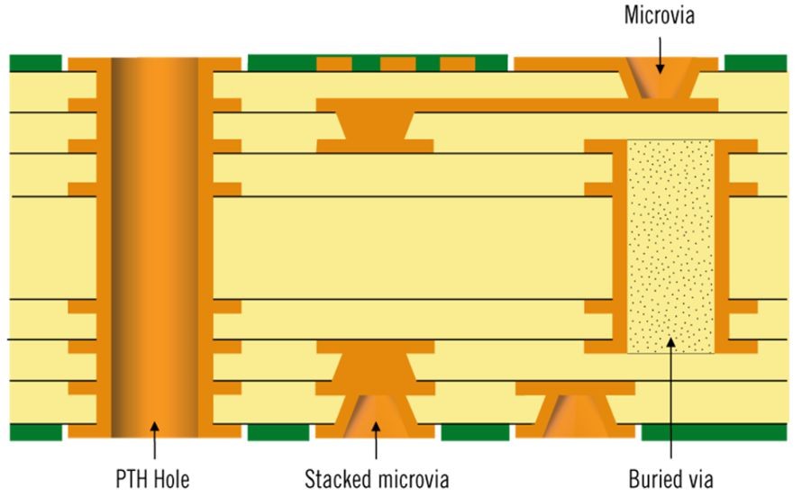
Types of Vias (Through, Blind, Buried)
The choice of via impacts both routing density and manufacturing cost.
Through-Hole Vias: Drilled through the entire board. They are cost-effective but create stubs on internal layers that can cause signal reflections.
Blind Vias: Connect an outer layer to one or more inner layers. They preserve precious routing area on the other side of the board.
Buried Vias: Entirely internal structures that connect inner layers without touching the surface. These are essential for complex, high-density layouts but increase fabrication complexity.
Microvias and HDI Design
High-Density Interconnect (HDI) technology is based on microvias, which are very small holes, usually laser-drilled to cross only one layer of the dielectrics. Microvias are the ideal solution for multi-gigabit interfaces such as PCIe Gen 5, as they are essentially without parasitic capacitance and no stubs.
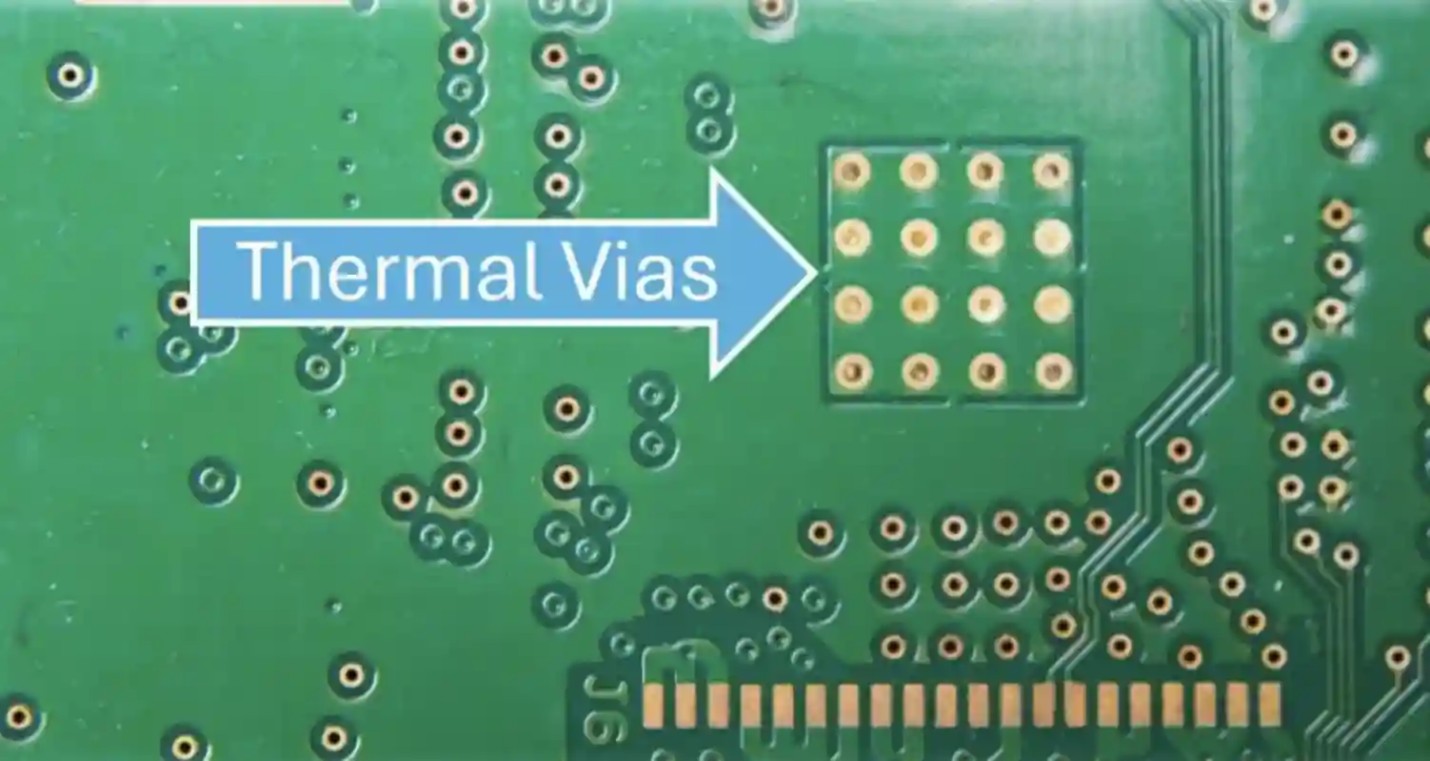
Thermal Relief and Heat Dissipation
Copper planes serve as lateral heat spreaders in a PCB multilayer application. To move heat vertically, engineers use thermal vias. These are arrays of through-holes placed directly under heat-generating components to pull thermal energy toward internal ground planes.
However, during assembly, solid copper connections can lead to cold joints. Thermal relief spokes provide sufficient thermal resistance for soldering while maintaining a reliable heat-dissipation path during operation.
Via Placement Optimization
Vias should be placed wisely so that it does not interrupt return paths. Avoid grouping vias too close together in small areas for ground planes, as this produces a Swiss cheese effect, which will raise the ground plane impedance and affect current flow. For thermal management, place via arrays in a grid pattern (typically 1.0-1.2 mm pitch) under power pads. To prevent solder wicking, these vias should be plugged with non-conductive epoxy and capped with copper.
Manufacturing and DFM Guidelines for Multi-layer PCB Design
The manufacturability of a board is crucial to its final quality. The Design for Manufacturability (DFM) process guarantees that your board can be manufactured with high yield, no costly changes, and reliability.
Design for Manufacturability (DFM)
Effective DFM is a link between digital CAD data and physical fabrication.
Aspect Ratio: Make sure the ratio of board thickness does not exceed 10:1 compared to the diameter of a drill. Too high an aspect ratio will make it hard for the manufacturer to plate copper evenly in the via barrel.
Annular Rings: Ensure a minimum ring of 0.15 mm (6 mils) around drills. This provides a safety margin for mechanical drill registration shifts during the lamination process.
Material Selection and Cost Control
Material choice is driven by thermal and frequency requirements. The standard FR-4 Tg 135 ℃-140 ℃ is used; however, for lead-free reflow, it is often necessary to use High-Tg FR-4 (170 ℃) to ensure that the laminate does not delaminate. Avoid unnecessary increase in the number of lamination cycles because each set of blind or buried vias will require another press cycle, thus raising the cost of the unit.
Assembly and Testing Considerations
A board that cannot be tested is a liability.
Fiducial Marks: Three global fiducials are to be placed on the board surface to guide automated pick-and-place machines.
Test Point Access: Each critical net must have a test point. Avoid using very small and fragile vias as probes or test points; use special pads for flying probe or bed-of-nails testing.
Common Design Mistakes to Avoid
Recurring errors are frequently found in diagnostic reviews that can slow down production:
Acid Traps: Do not use a trace junction with an acute angle, as it will collect etching chemicals and cause over-etched and brittle traces.
Symmetry Issues: Always maintain a symmetric multilayer PCB stackup. A non-uniform copper weight will lead to warping of the board in the reflow oven.
Footprint Inversion: Double-check the bottom view component pinouts. Mirroring a footprint is a classic error that renders the first batch of prototypes useless.
Multilayer PCB Design Checklist
Before submitting your design, verify the following:
| Checklist Item | Requirement / Target |
|---|---|
| Stackup Symmetry | Copper weights mirrored across the center core |
| Reference Continuity | High-speed signals do not cross GND plane splits |
| Return Vias | Stitching vias present at all layer transitions |
| 3W Spacing | Applied to all clocks and data strobes |
| Annular Ring | 0.15 mm minimum |
| Fiducials | Three global fiducials present on each surface |
Conclusion: Multilayer PCB Design Guidelines
Mastering multilayer PCB design guidelines requires viewing the board as a precision transmission environment. Success is built on a symmetric, reference-heavy stack-up and on signal return-path continuity. By putting physics first, engineers avoid signal integrity issues and mechanical problems, ensuring reliable high-performance PCB designs.
FAQ about Multilayer PCB Design Guidelines
Q: When do I need high-Tg?
If you have lead-free board assembly or your board will be operating in a high-temperature industrial setting, choose a high-Tg 170 ℃ to avoid delamination or via cracking.
Q: Is it OK to route a high-speed signal over a power plane?
Yes, but power planes are noisier than ground planes. You must ensure the plane is continuous and properly decoupled to ground at both ends to provide a path for return currents.
Q: Why are odd layer counts discouraged?
Odd layer counts (like 5 or 7) are structurally unbalanced. Manufacturers typically build them as the next even number to prevent severe warpage during lamination.
Keep Learning
BGA PCB Design Complete Guide: Layout and Routing Guidelines
Key Takeaways Define pad type first: Always confirm SMD or NSMD pad strategy before routing BGA fanout. NSMD is generally preferred for better solder joint formation, while SMD suits very small pads or tight mask registration. Match the process to the pitch: 0.8 mm BGAs work with dog-bone fanout and standard vias; 0.5 mm BGAs typically need via-in-pad or HDI routing. Picking the right via strategy early saves layers and cost. Place decoupling capacitors on the bottom side: Mount MLCCs directly under t......
PCB Design Rules and Guidelines: A Complete Best Practices Guide
A great schematic is just an idea. To turn it into a real, working product, you need to follow a robust set of Printed Circuit Board Design Rules. Ignoring these rules leads to costly respins, signal integrity (SI) failures, and boards that are physically impossible to build. This guide is a technical resource for the entire design process. We'll cover the essential rules for schematics, layout, and manufacturing that every engineer and hobbyist needs to know for a successful design. What Are PCB Desi......
Mastering PCB Design: A Step-by-Step PCB Layout Process Guide
Key Takeaways Process over improvisation: A repeatable, standardized PCB layout process—not luck—is what turns a working schematic into a board that succeeds on the first spin. Placement drives everything: Component layout and functional block partitioning are the most impactful steps; good placement makes routing easy, poor placement makes it impossible. Route critical signals manually first: Clocks, differential pairs, sensitive analog nets, and power switching loops must be hand-routed before auto-......
Multilayer PCB Design Guidelines: Stack-up and Layout Best Practices
Key Takeaways Stack-up is the foundation: The layer arrangement defines signal integrity, impedance control, and EMI performance — plan it before routing a single trace. Symmetric, reference-heavy designs prevent failures: A balanced stack-up with ground planes adjacent to every signal layer avoids warpage, ensures return path continuity, and minimizes crosstalk. DFM rules ensure manufacturability: Aspect ratio, annular rings, material selection, and symmetric copper distribution are critical to produ......
How to Reduce Noise and EMI in PCB Layout: A Comprehensive Design Guide
Key Takeaways EMI origins: EMI stems from structural layout deficiencies — poor return paths, interrupted reference planes, and large loop areas create antenna structures that radiate unwanted energy. Loop area is critical: Minimizing current loop areas through solid ground planes adjacent to signal layers is the single most effective EMI reduction technique. Placement defines noise: Component placement establishes current loops before routing. Group by function (power, analog, digital, RF), isolate a......
What is the Difference Between PCB Design and Layout?
The difference between PCB design and PCB layout trips up more engineers than you’d expect. While often used interchangeably, these are distinct disciplines. The gap between them is where many projects quietly go sideways. Simply put, PCB design is the logical foundation, while PCB layout is the physical implementation. A flawless schematic can fail in production due to poor layout, and even the best layout engineer can’t rescue it. Below, we provide a detailed breakdown of the differences between the......