How to Read and Create PCB Schematics
17 min
- What is a PCB Schematic?
- Common Components in a Schematic Design:
- How to Read and Interpret a Schematic Diagram
- Steps to Create a PCB Schematic in EasyEDA
- Tips for Efficient Schematic Design
- From PCB Schematic to Manufacturing
- Troubleshooting with Schematics
- FAQs about PCB Schematics
- Conclusion
Key Takeaways
- Read Schematics: Understand symbols, net labels, and component values.
- Design in EasyEDA: Place components and create circuit connections.
- Run Design Checks: Use ERC and DRC to identify potential issues.
- Verify Components: Check pin assignments and PCB footprints.
- Prepare for Manufacturing: Validate PCB layouts and manufacturing files.
Printed circuit board (PCB) design begins with a clear understanding of how the electronic circuit should function. A schematic diagram represents the circuit using standardized symbols, component references, values, and electrical connections called nets. It allows engineers to review circuit logic, trace signal paths, and identify potential design issues before moving on to PCB layout.
A well-organized schematic also improves communication among designers, hardware engineers, and manufacturing teams. By documenting component connections and design intent clearly, it provides a reliable starting point for PCB layout, verification, and production preparation.
EasyEDA provides a convenient environment for creating and reviewing electronic schematics and developing PCB layouts. In this article, we explain how to read a PCB schematic, identify common circuit symbols, and create a schematic in EasyEDA. We also cover practical design checks that help reduce connectivity errors and prepare a design for the next stage of PCB development.
What is a PCB Schematic?
A PCB schematic is a graphical representation of an electronic circuit. It uses standardized symbols to represent components such as resistors, capacitors, diodes, and integrated circuits (ICs), while wires and net labels show their electrical connections. Component designators and values provide additional information needed to understand the circuit.
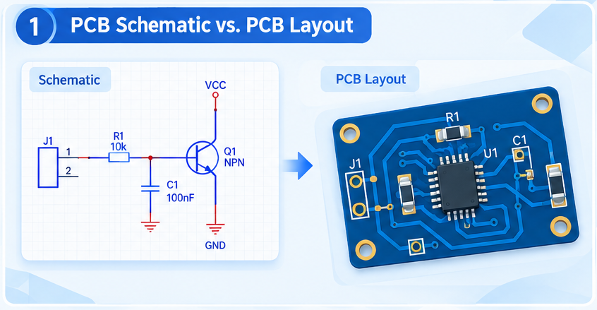
A schematic describes electrical connectivity and circuit logic, not the physical placement of components or the copper traces on a board. PCB layout translates the verified circuit connections into a physical design by assigning footprints, arranging components, routing traces, and defining board geometry. Keeping these two stages distinct helps designers identify electrical and physical design issues more effectively.
Standard symbols enable schematics to simplify even the most complex systems, therefore facilitating engineers and designers in communicating their ideas. In electronics design, schematic drawings are also rather crucial since they enable the identification of issues before they become evident during the assembly process.
Common Components in a Schematic Design:
1. Schematic Symbols
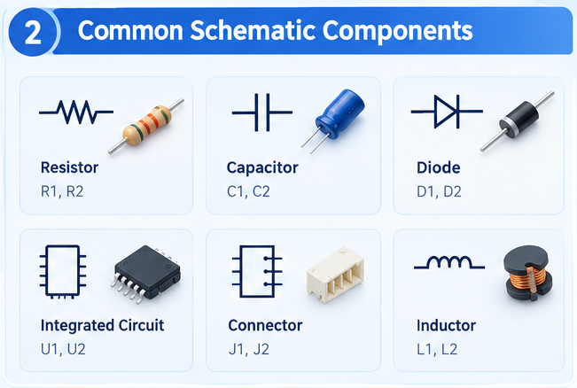
Before diving into a schematic, familiarize yourself with the common symbols:
● Resistors: Common schematic symbols use either a zigzag line or a rectangular shape, depending on the drafting convention.
● Capacitors: A non-polarized capacitor is typically shown with two parallel plates. A polarized capacitor uses a symbol or marking that indicates polarity; verify the positive and negative terminals where applicable.
● Diodes: A diode symbol consists of a triangle-free diode shape with a bar indicating the cathode. Check the symbol orientation and the anode/cathode markings to determine the intended current direction. The exact graphical representation may vary by diode type and schematic convention.
● Integrated Circuits (ICs): IC symbols show pins and their associated names or numbers. Depending on the design, one physical IC may be represented by a single symbol or multiple functional units.
● Ground and Power Symbols: Symbols such as GND and VCC identify named power or reference nets. Different ground symbols or power labels do not necessarily mean the nets are electrically connected; verify the schematic's net connectivity.
2. Following Nets (Connections/wires)
Wires represent electrical connections between component pins, while net labels identify connections by name. In many EDA tools, points carrying the same net name are treated as electrically connected within the applicable schematic scope, even when no continuous wire is drawn between them.
When reading a schematic, check wire endpoints, junction dots, net labels, and power symbols carefully. A line crossing does not always indicate an electrical connection; the junction marker and the tool's drawing conventions determine whether the nets are connected.
3. Component Values and Designators
Each component is identified by a unique reference designator, such as R1 for a resistor, C1 for a capacitor, or U1 for an integrated circuit. Its value or part number describes its electrical characteristics or identifies the specific device. For example, a resistor may be marked as 10 kΩ and a capacitor as 100 µF.
These details should not be confused with the component footprint. The value describes the component's electrical specification, while the footprint defines its physical pad arrangement and mounting dimensions on the PCB. Before moving to PCB layout, verify that each selected component has an appropriate footprint and that the footprint matches the intended part's datasheet.
| Component | Common Designator | Information to Check |
|---|---|---|
| Resistor | R1, R2 | Resistance value, tolerance, and power rating |
| Capacitor | C1, C2 | Capacitance, voltage rating, and polarity where applicable |
| Diode | D1, D2 | Anode/cathode orientation and device specifications |
| Integrated Circuit (IC) | U1, U2 | Part number, pin assignments, and required operating conditions |
| Connector | J1, J2 | Pin numbering, pin functions, and connection polarity where applicable |
| Inductor | L1, L2 | Inductance, current rating, and relevant datasheet specifications |
How to Read and Interpret a Schematic Diagram
A schematic may contain several functional blocks, such as power input, voltage regulation, control logic, and output interfaces. Although diagrams are often arranged from left to right or top to bottom for readability, this layout is a visual convention rather than a rule of electrical operation. To interpret a circuit correctly, follow the net connections, component pin assignments, and relevant datasheet specifications instead of relying on visual position alone.
The example schematic is organized into four functional blocks: input, main IC, charge control, and output. The accompanying description identifies a lithium-ion battery charging application with a stated maximum charging current of 1.5 A. Before using this example as a design reference, verify the battery configuration, charger IC specifications, input voltage range, charging-current setting, and protection requirements against the actual schematic and component datasheets.
Section 1: Input
The two-pin connector provides the circuit's external input connection. The capacitors connected to the input net may serve as local bypass or bulk capacitors, depending on their values, placement, and the circuit design. The VIN net label can connect this input net to other parts of the schematic without drawing a long wire across the page.
When reviewing this block, confirm the connector pin assignments, input polarity, voltage rating of the capacitors, and the charger's permitted input-voltage range. Also check the recommended input-capacitor values and placement in the charger IC datasheet.
Section 2: Main IC
The main IC should be identified by its exact part number, and its symbol pin names and numbers should be checked against the manufacturer's datasheet. The schematic shows two LEDs intended to indicate charging status; their actual functions depend on the IC's status outputs and the surrounding circuitry.
Before proceeding, verify the supply pins, ground connections, enable or control pins, status outputs, and any required pull-up or pull-down resistors. Confirm that the schematic symbol's pin mapping matches the selected component and that all required connections follow the datasheet's application circuit.
Section 3: Charge Control
The charge-control block implements the charging and power-conversion functions defined by the selected charger IC. If the circuit uses a switching buck topology, the inductor, switching device, diode (where required by the topology), and capacitors work together to transfer energy and filter voltage and current ripple. The exact role of each component must be confirmed from the schematic and the IC datasheet.
The resistor labeled R10_CC_CTRL may be associated with charge-current programming, as suggested by its name in the original description. However, its function and the stated 1.5 A setting must be verified against the IC's programming equation and the actual component value. Also check the recommended inductor value, capacitor specifications, current ratings, and PCB layout requirements to support stable operation and thermal performance.
Section 4: Output
The output connectors provide the intended battery or load interfaces, as defined by the schematic. If the design supports both 1S and 2S battery configurations, verify that the charger IC, charging-voltage settings, protection circuitry, and component voltage ratings are compatible with each supported configuration.
A 1S lithium-ion pack typically contains one cell in series, whereas a 2S pack contains two cells in series and therefore requires a different charging-voltage profile. Do not assume that a connector or selector alone makes a charger compatible with both configurations. Confirm the intended operating modes and all required circuit changes from the schematic and the charger IC datasheet before presenting this design as supporting both 1S and 2S batteries.
Steps to Create a PCB Schematic in EasyEDA
Step 1: Sign Up and Start a New Project
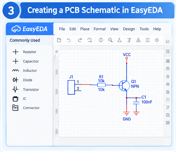
Open EasyEDA and create a new project using the available project-creation options. Create or open a schematic document within the project, and give the project and document clear, descriptive names. Keeping related design files organized makes it easier to review revisions and move from schematic capture to PCB layout.
Step 2: Place Components
Search the component library for the required symbols and add them to the schematic. Before using a library component, verify its part number, symbol pin names, pin numbers, and electrical properties against the manufacturer's datasheet.
Where the design will proceed to PCB layout, also check whether an appropriate PCB footprint is available and whether its pad numbering matches the symbol's pin mapping. If the exact component or footprint is unavailable, select a verified alternative or create the required library item using the manufacturer's documentation.
Step 3: Connect Components
Use the wire tool to connect component pins according to the intended circuit and the reference design in the datasheet. Apply clear net labels to important power rails, grounds, control signals, and interfaces where appropriate.
After wiring, check for unconnected pins, unintended junctions, duplicated or inconsistent net names, and incorrect power connections. For connections made through net labels rather than continuous wires, confirm that the labels refer to the intended nets under the EDA tool's connectivity rules.
Step 4: Annotate the Schematic
Assign unique reference designators to components, such as R1, C1, and U1, using the annotation function when available. Add component values, relevant part numbers, connector pin descriptions, and concise notes where they help clarify circuit behavior.
Before finalizing the schematic, check for duplicate designators, missing component values, inconsistent labels, and notes that conflict with the actual circuit. Keep comments concise and ensure that the documentation reflects the current design revision.
Step 5: Perform Electrical Rule Check (ERC)
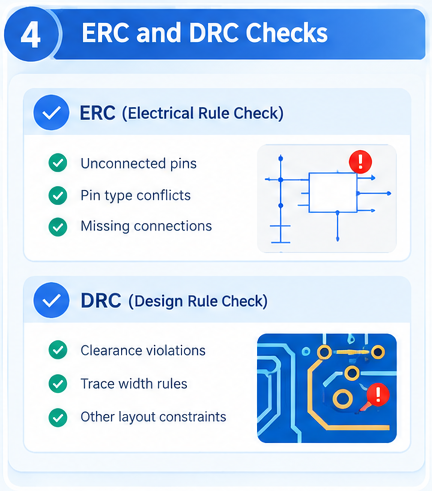
Run the schematic editor's Electrical Rule Check (ERC) to identify potential electrical connectivity and rule violations, such as unconnected pins, conflicting pin types, or missing required connections, depending on the tool's rules and settings. Review each reported error and warning instead of dismissing them automatically.
ERC does not prove that a circuit will function correctly, and it does not replace PCB-level Design Rule Checking (DRC). After transferring the design to PCB layout, run DRC to check applicable physical design constraints, such as copper clearances, trace widths, and other manufacturing-related rules. Resolve or document relevant issues before generating manufacturing files.
Step 6: Save and Share
Save the project and keep its schematic and associated design documents organized. Depending on the intended use, export a readable schematic document for review or share the editable project with collaborators.
When the schematic is ready, proceed to PCB layout by assigning and verifying footprints, arranging components, and routing the board. A schematic PDF or image is useful for documentation and review, but it is not a substitute for the PCB fabrication files required by a manufacturer. The required production outputs should be generated from the completed PCB design and checked before ordering.
Tips for Efficient Schematic Design
A well-organized schematic makes circuit behavior easier to review, debug, and transfer to PCB layout. Apply the following practices when creating or revising a design.
Organize Functional Blocks: Group related circuitry, such as power input, regulation, control, and interfaces. Use descriptive section headings where appropriate to make the signal and power flow easier to follow.
Use Clear Net Names: Apply consistent names to important power rails, grounds, control signals, and interfaces. Check that repeated labels connect only the nets intended by the design.
Keep Connections Readable: Minimize unnecessary wire crossings and long, confusing connections. Use junction markers and net labels according to the EDA tool's conventions, and verify ambiguous connections before running ERC.
Maintain Consistent Annotations: Use unique reference designators, readable component values, and clear pin labels. Avoid overlapping text and symbols that make the circuit difficult to review.
Verify Components and Footprints: Cross-check important component values, part numbers, pin mappings, and PCB footprints against datasheets before moving to layout.
Use Grid Alignment Where Helpful: Align symbols and wires consistently to improve readability. Grid snapping is a useful editing aid, but it does not guarantee correct electrical connectivity or PCB manufacturability.
Run Checks After Revisions: Repeat ERC after significant schematic changes. Once the PCB layout is created, perform DRC and review the resulting manufacturing files as separate verification steps.
| Review item | What to verify | Why it matters |
|---|---|---|
| Component selection | Part number, electrical ratings, and datasheet requirements | Helps avoid incorrect or unsuitable components |
| Pin mapping | Symbol pin numbers and functions match the datasheet | Reduces the risk of incorrect connections |
| Net connectivity | Wire endpoints, junctions, net labels, and power connections | Helps identify unintended or missing connections |
| Component footprints | Pad numbering, package dimensions, and mounting requirements | Supports correct PCB layout and assembly |
| Electrical checks | ERC errors and warnings are reviewed | Identifies potential schematic-rule violations |
| PCB design checks | DRC rules, trace widths, clearances, and applicable constraints | Helps identify layout issues before fabrication |
| Manufacturing files | Gerber layers, drill data, board outline, and final revision | Helps ensure the exported data matches the intended board |
From PCB Schematic to Manufacturing
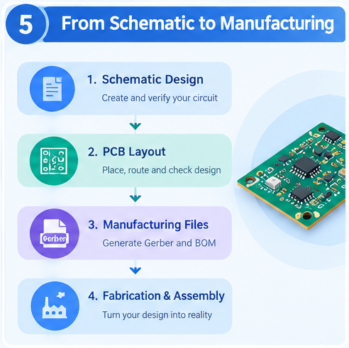
A completed schematic is an important milestone, but it is only one stage of PCB development. Before a circuit can be manufactured, its electrical connections must be translated into a physical board layout, checked against the intended design, and exported in the required production formats.
1. Verify the Schematic and Component Footprints
Before starting PCB layout, confirm that the schematic has no unresolved connectivity issues and that important component values and pin assignments match the relevant datasheets. Assign the correct PCB footprint to each component and verify pad numbering, package dimensions, and mounting requirements.
A symbol-to-footprint mismatch can cause assembly problems even when the schematic's electrical connections appear correct.
2. Complete PCB Layout and Design Rule Checks
During PCB layout, arrange components and route copper traces while considering board dimensions, connector accessibility, power distribution, thermal behavior, and signal integrity. The applicable design rules depend on the circuit requirements and the selected manufacturing process.
Run PCB Design Rule Checking (DRC) to identify rule violations, such as insufficient clearances or trace widths outside the configured constraints. For power and high-speed circuits, additional review of current paths, grounding, return paths, and controlled-impedance requirements may be necessary.
3. Prepare and Review Manufacturing Files
After the PCB layout is complete, generate the manufacturing files required for the selected service. These commonly include Gerber data for the relevant board layers and drill files for hole locations and sizes. Additional files may be required for particular fabrication or assembly services.
Before placing an order, review the exported data in a Gerber viewer. Check the board outline, copper layers, solder mask, silkscreen, drill locations, and other applicable features against the intended design. Confirm that the exported files reflect the final PCB revision.
4. Check the Design Against Manufacturer Capabilities
PCB design rules should be evaluated against the selected manufacturer's current capabilities, board specifications, and process requirements. Trace width, spacing, drill size, layer count, material selection, and controlled-impedance requirements can affect whether a design is suitable for the intended manufacturing process.
Reviewing these constraints before ordering helps identify potential manufacturability issues earlier and reduces the risk of avoidable design revisions.
A reliable transition from schematic to manufacturing therefore requires more than a successful ERC result. Schematic verification, footprint validation, PCB layout checks, and manufacturing-file review all contribute to a more consistent design handoff.
Troubleshooting with Schematics
A schematic helps engineers understand intended circuit behavior and identify where to investigate when a board does not operate as expected.
Trace the Relevant Circuit Block: Start with the affected function, such as the power input, regulator, control circuit, or output interface. Follow the relevant nets and check the connections against the intended design.
Review Component Specifications: Verify component values, polarity, pin assignments, and datasheet requirements. Incorrect component selection or pin mapping can produce symptoms that resemble a connectivity fault.
Compare Expected and Measured Values: Use the schematic and datasheet to determine expected voltage and current ranges at relevant test points. Measure the physical board using appropriate instruments and safe procedures, then compare the results with the expected behavior.
Inspect the Physical Board: If the schematic appears correct, examine the assembled board for soldering defects, damaged components, incorrect assembly, or physical connection problems. These issues cannot be confirmed from the schematic alone.
Recheck the Design After Changes: If troubleshooting leads to a schematic revision, update the design documents and rerun the relevant electrical and PCB-level checks before preparing a new production revision.
FAQs about PCB Schematics
Q: What Is the Difference Between a PCB Schematic and a PCB Layout?
A PCB schematic shows the circuit's components and their electrical connections. A PCB layout defines the physical arrangement of components, copper traces, pads, and board geometry. Both are necessary stages of PCB development.
Q: Can I Create a PCB Schematic in EasyEDA?
Yes. EasyEDA provides schematic design tools for placing component symbols, connecting pins, naming nets, and checking electrical rules. Before moving to PCB layout, verify component specifications, pin mappings, and available footprints.
Q: What Is the Difference Between ERC and DRC?
ERC checks electrical connectivity and schematic rules, depending on the tool's rule settings. DRC checks PCB-level design constraints, such as trace widths and clearances. Neither check guarantees that a circuit will function correctly or that every manufacturing issue has been eliminated.
Q: Why Must PCB Footprints Be Checked Before Layout?
A footprint defines the physical pad arrangement and dimensions used to mount a component on the PCB. If the footprint or pad numbering does not match the intended component, the board may have assembly or connectivity problems even when the schematic is correct.
Q: Are Schematic Files Enough to Manufacture a PCB?
Not usually. A schematic documents circuit connectivity, while PCB fabrication generally requires manufacturing data generated from the completed PCB layout, including the relevant Gerber layers, drill data, and board outline. The exact file requirements depend on the selected manufacturing service.
Conclusion
A clear and accurate PCB schematic is essential for understanding circuit behavior, reviewing electrical connections, and preparing a design for PCB layout. Consistent net naming, correct component values, verified pin assignments, and organized functional blocks make schematics easier to read, maintain, and troubleshoot.
When creating a schematic in EasyEDA, use the component datasheets to verify important connections and run ERC to identify potential electrical-rule violations. Before proceeding to manufacturing, also validate component footprints, complete PCB layout checks, and review the exported manufacturing files against the intended design and the manufacturer's current requirements.
By treating schematic capture, PCB layout, and manufacturing-file preparation as connected but distinct stages, designers can improve design clarity, identify issues earlier, and create a more reliable handoff from circuit design to PCB production.
Popular Articles
• The Comprehensive Guide to Circuit Symbols: Key to Understanding Electrical and Electronic Diagrams
• Design Guidelines for PCB Using FR4 Substrates
• Choosing the Best PCB Color-Enhancing Aesthetics and Functionality
• PCB Silkscreen: All You Need to Know
• PCB Board Design: A Step-by-Step Guide for Beginners
Keep Learning
How to Read and Create PCB Schematics
Key Takeaways Read Schematics: Understand symbols, net labels, and component values. Design in EasyEDA: Place components and create circuit connections. Run Design Checks: Use ERC and DRC to identify potential issues. Verify Components: Check pin assignments and PCB footprints. Prepare for Manufacturing: Validate PCB layouts and manufacturing files. Printed circuit board (PCB) design begins with a clear understanding of how the electronic circuit should function. A schematic diagram represents the cir......
Maximizing Circuit Reliability with PCB Test Points and Smart DFT
Key Takeaways Early Fault Catching: Test points drastically reduce diagnosis time and prevent costly field failures. Standard Pad Sizing: Use 1.0 mm flat copper pads with 2.54 mm spacing for optimal fixture contact. Protect High-Speed Signals: Keep branch traces short to prevent capacitive loading and resonance. Single-Sided Access: Place all test pads on the bottom layer to cut fixture costs. Right Test for Volume: Use flying probe for prototypes and bed-of-nails ICT for mass production. A PCB test p......
The Comprehensive Guide to Circuit Symbols: Key to Understanding Electrical and Electronic Diagrams
Note Need a quick reference while reading schematics? Download our free, printable Circuit Symbols Cheat Sheet (PDF), featuring the most common IEC and ANSI symbols organized by category. Keep it on your desktop or print it for easy reference at your workbench. ⬇ Download the Free Circuit Symbols Cheat Sheet (PDF) Every electronic diagram is written in a visual language, and circuit symbols are its alphabet. From your first electrical schematic to a multi-layer board, knowing circuit symbols can make ......
Design Guidelines for PCB Using FR4 Substrates
Material substrate concerns are necessary while designing electrical circuit boards. This is due to the fact that printed circuit boards cannot be manufactured without the appropriate PCB materials. When developing and producing circuit boards, the substrate material must be taken into account just as much as the copper layers, silkscreen, and surface polish. Generally speaking, non-conductive materials like porcelain, Marlon, FR4, and the like must be used for PCB substrates. Depending on its intende......
Choosing the Best PCB Color-Enhancing Aesthetics and Functionality
Key Takeaways Choosing the best PCB solder mask color involves balancing aesthetics, visibility, and functionality. Green remains the top choice for superior contrast and inspection, while black offers premium appeal, white excels in LED applications, and other colors like purple and red provide unique design options. The ideal color depends on your priorities in inspection ease, thermal performance, and brand image, with minimal impact on electrical performance when using proper silkscreen contrast. ......
4 Layer vs 6 Layer vs 8 Layer PCB: How to Choose the Right Stackup
Random selection of layers in electronics may lead to serious signal integrity issues. That's why we always design our stackup before designing the PCB. Stackup decides the type of PCB and how it gonna perform under high-frequency conditions. There are a lot of things that directly affect the stackup of the PCB, related to impedance matching, routing density, signal and power integrity, electromagnetic compatibility (EMC), and cost. Knowing the requirements before design and the most critical componen......