Unlocking Flexibility and Scalability with Daughter Boards in Modern Electronics
14 min
- Understanding Daughter Boards in PCB Design
- Major Benefits of Using Daughter Boards
- Design Best Practices for Daughter Board Systems
- From Modular Design to Manufacturing Success
- JLCPCB's Expertise in Supporting Daughter Board Projects
- FAQ about Daughter Board
- Conclusion
Key Takeaways
- Daughter boards add flexibility and scalability without redesigning the main PCB.
- Enable easy upgrades for memory, wireless, sensors, and I/O modules.
- Reduce development time, costs, and maintenance efforts significantly.
- Proper connector selection and mechanical design are essential for reliability.
- Ideal for modular products like Raspberry Pi HATs and Arduino shields.
Have you ever removed the back of a laptop, stuck in a piece of RAM, and watched it boot with extra memory a minute later? It's the little upgrade due to a daughter board, which is a plug-in circuit board that fits into a larger host board, and immediately expands the capabilities of the system. So no need to install a new computer, or even the whole module; you just simply added a module. There is a vast amount of modern equipment that revolves around that one thought.
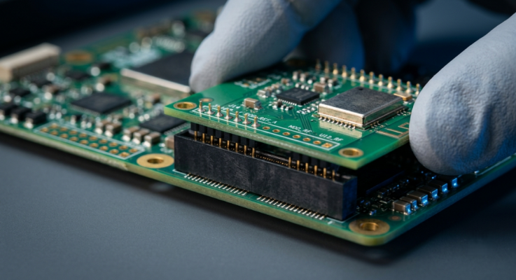
From Raspberry Pi HATs to Arduino shields, to SODIMM memory sticks, Wi-Fi cards, and industrial I/O modules. This means that the product ranges can be expanded without a complete redesign, which makes the development faster, and the repair is less expensive. We'll explore here what a daughter board is, how it is different from the motherboard, the actual advantages it offers, and how and what goes into creating a reliable multi-board system. Knowing what daughter boards are and what they can do will help the design be more flexible and so much easier to scale when building a sensor module or building a stackable compute platform.
Understanding Daughter Boards in PCB Design
A daughter board is not a product by itself; it's a half partnership. It is important to know what it can do by itself and what it can do when attached to the host board it plugs into.
What a Daughter Board Is and How It Works
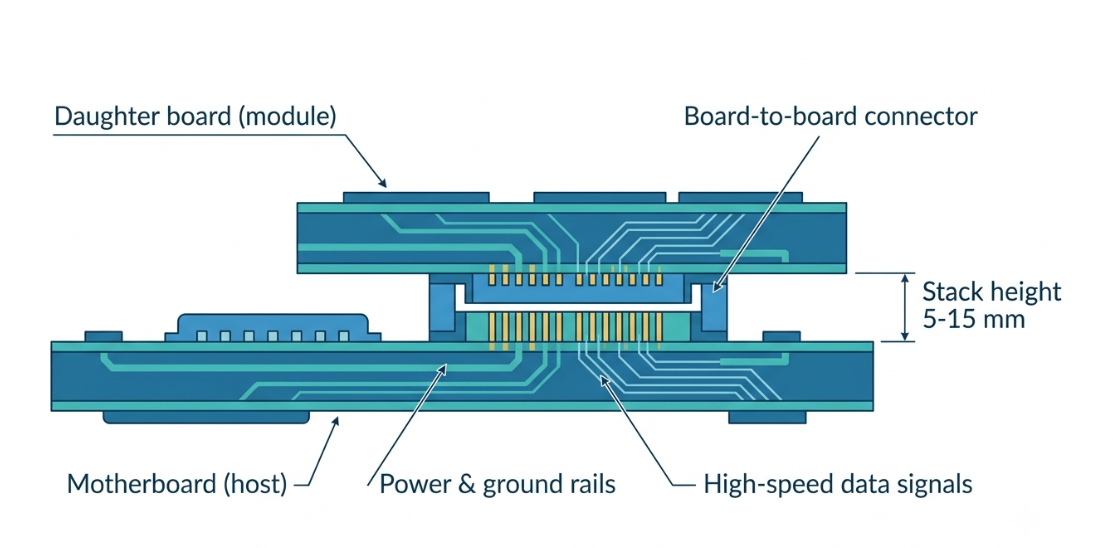
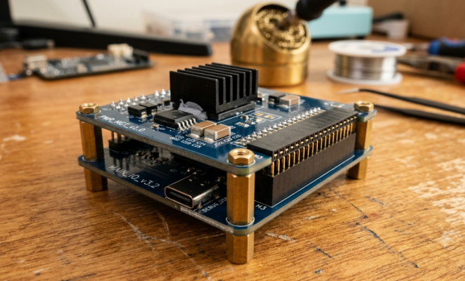
A daughter board (also known as daughter card, mezzanine board, or piggyback board) is a secondary board attached to a larger main board to provide additional or supplemental features. It uses power and sends signals via the host; it is normally not able to function independently. It's like a specialized attachment; the host is the base, and the heart of the system is the connection. A daughter board mates to host via a defined interface. It is typically either a board-to-board connector, a card-edge slot, or a mezzanine header. It is a connector that has to accept power rails, ground, clocks, and data signals, and requires the correct choice for both electrical characteristics and mechanical fit. A daughter board is a common task that is performed by:
- Adding a radio (Wi-Fi, Bluetooth, LoRa, or cellular) to a base system
- Adding memory or storage, such as SODIMM or M.2 modules.Expansion of memory or storage as SODIMM or M.2 modules.
- Designing sensor front-ends, analog acquisition, or motor drive
- Separating connectors and I/O, which are product-dependent.Decoupling connectors and I/O between products.
The module is modular and can be designed, tested, and certified once, then used on numerous host boards. That re-use is what makes a one-off circuit scalable into a building block.
Motherboard vs Daughter Board: Key Differences and Use Cases
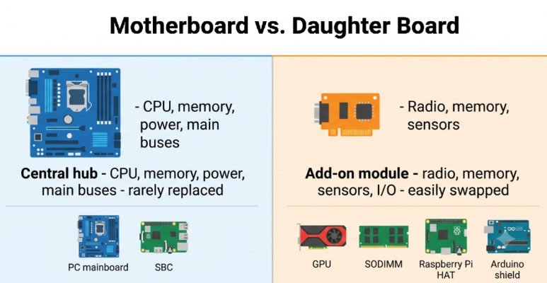
The motherboard is the main component of a system. It holds the primary buses that connect everything, the power tree, the memory controller, and the main processor. All the rest is connected with it, either directly or indirectly. A daughter board, on the other hand, is a peripheral extension that connects to that hub to provide a certain functionality. The best method to view the relationship between the Motherboard and Daughter Board is side by side.
| Aspect | Motherboard | Daughter Board |
|---|---|---|
| Role | Central hub and core logic | Add-on module for extended features |
| Size | Larger defines the form factor | Smaller, fits onto or beside the host |
| Function | Hosts CPU, memory, power, and main buses | Adds radio, memory, sensors, or I/O |
| Replaceability | Rarely replaced; costly to change | Easily swapped or upgraded |
| Examples | PC mainboard, SBC base, controller board | GPU card, SODIMM, Raspberry Pi HAT, Arduino shield |
Major Benefits of Using Daughter Boards
Enhanced Modularity, Maintainability, and Upgradeability
The major advantage is modularity. Separating a function onto its own board isolates it from the rest of the system, allowing it to be developed and tested separately. If the radio module does not pass certification or if a sensor becomes obsolete, you only touch that board, and the motherboard remains untouched. The same boundary makes field service much easier. The flawed daughter board is quickly unplugged and replaced, which means no fine pitch parts are reworked on the main assembly.
For products on the ground, it can be the difference between a 5-minute swap and a full board return. If another interface becomes available or a new sensor is available, you issue a new daughter board with the same connector and physical form factor. Your engineering work remains on the part that has changed, and the customer's underlying hardware continues to function.
Cost Reduction Through Reuse and Simplified Main Boards
The savings also make more sense at scale, and daughter boards are also cost-saving. If one certified module is used for multiple products, you divide the module design, tooling, and certification costs amongst the multiple products it is used for. That's where modular architectures make their return; it will also make the primary board less expensive. The optional features are available on daughter boards, and the motherboard only has what all configurations require. A customer who is buying the base model pays for the radio, additional memory, and premium I/O they will never use. Take into account the realistic cost logic:
- Design once, deploy many: One sensor daughter board can be used on an entire product family.
- Reduce inventory risk: Inventory of modules, not finished boards, and less risk of absorption if demand changes.
- Less costly repairs: Better to replace a small module than a large, tightly-packed assembly.
Design Best Practices for Daughter Board Systems
A daughter board is only as good as the interface that connects. If the connector, power, and mechanics are correct, then the system seems to be seamless.
Interface Selection, Connector Choice, and Signal Integrity
The board-to-board connector is the most crucial design choice. Mezzanine connectors are available in discrete stack heights typically ranging from 5 mm to 15 mm, meaning the height of the stack will also be the height of the connector.
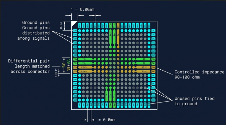
The connector can be used as any other transmission-line discontinuity for high-speed links. Maintain the controlled-impedance traces (typically 50 Ohms single-ended, 90 to 100 Ohms differential) across the interface and provide a clean return path for all signals through adjacent ground pins. Grounds are used around fast signals to confine the return current. A good rule of thumb is to use grounds around fast signals in the connector pinout. This is the interface of the watch, these signal-integrity essentials:
- Use lots of ground pins and try to spread them out on the signals, and not only at the ends.
- Match lengths of differentials on the connector, taking into account the skew of the connector itself.
- Do not send high-speed nets across the mating gap without any reference plane on either board.
- Don't leave unused pins floating.
Power Distribution, Mechanical Alignment, and Thermal Management
Power must also traverse the connector, and the connector's pins have actual current limits. Install multiple pins on each high-current rail, size the pins against the manufacturer's derating curve, and install bulk and high-frequency decoupling capacitors on the daughter board close to the loads. The connector should place the board, but not provide all the support in terms of mechanics. Install vibration and insertion force stops by mounting standoffs to prevent fatigue of solder joints.
A daughter board may become a thermal barrier against the host, or it may obstruct airflow; it may be intentionally designed to create the thermal path. Under power components, use thermal vias; ensure that tall components are not in the mating area; verify that there is clearance for any heatsink or thermal pad that you are depending on.
Hierarchy Planning and Standardization for Reusability
Standardization is the actual power of daughter boards. Once you set the one connector pinout, one power scheme, and one mechanical footprint, any future module based on the spec will fit right into place. Raspberry Pi HATs and Arduino shields are popular for just this reason: they have fixed and public interfaces. Always route things before you plan the hierarchy. Determine what functions should be on the motherboard, on daughter boards, and how far it will be stacked. Next, freeze the interface contract (pinout, voltage levels, mechanical outline, and keep-outs) and document it such that all future boards and all team members build to the same point of reference.
From Modular Design to Manufacturing Success
Impact on Panelization, DFM, and Production Efficiency
The approach to panelizing a product will differ if it is divided into a motherboard and daughter boards. Smaller plug-in modules can panelize effectively into their own arrays, typically by V-scoring or tab routing, and are then powered by the larger host board. By matching the fiducials and tool holes on each board to the standard DFM rules, both are flowing through pick and place without special fixturing. Special DFM consideration should be given to connectors. Board-to-board headers are frequently tall, dense, and press fit or through hole, check courtyards, insertion clearances, and paste apertures early. If the slot of a connector is just too close to the edge of a board or below the connector of a taller neighbor, it can derail an otherwise perfect assembly line.
When planned for, modularity can actually increase production efficiency:
- Use high-volume daughter boards on specialized, optimized panels and profiles.
- Test each module before mating, to ensure that any faults are discovered on the cheaper board.
- Reduce the number of parts on the motherboard, which shortens the assembly time.
Common Pitfalls and How to Avoid Them During Handover
The most hazardous time is handover, when your design files get to the fabricator and assembler. On the bench, projects fail here less than multi-board projects. Typically, it is a small mismatch that is easy to avoid, which leads to failure. Identify the following common challenges:
- Orientation errors in connectors: Parts are mirrored or rotated, but do not connect to each other during DRC. Check the mated pair in 3D and not just one board.
- Stack-height mismatch: A connector of a different height than the standoffs, causing the board to tilt or not to stand up.
- No mating docs provided: Send two boards with no drawing that shows how the pieces fit together, assemble, and assume what they should be used for.
- Incomplete BOM or CPL data: A plug-in module was sent with the incorrect gender of the connector or sent with a misaligned centroid data file.
You don't want to be involved in any of them, because you want to consider the stack you've assembled to be your actual product. Include clear assembly drawings, label the interface, and provide the necessary orientation for the manufacturer to assemble what you want.
JLCPCB's Expertise in Supporting Daughter Board Projects
Professional DFM Review Optimized for Modular Architectures
All orders at JLCPCB must go through an engineering DFM check before they can be produced. That review process is where daughter board projects can find issues such as small courtyards for connectors, press-fit connectors with edging, and clearance around drill and annular ring parts. They are collected on the host board and the module, thus avoiding the need for an expensive respin. With JLCPCB's instant quoting and EasyEDA integration, you can make a change to a connector footprint or panel layout and re-quote it in minutes to keep your multi-board project on track.
Advanced Manufacturing Capabilities for Complex Multi-Module Boards
Daughter boards may require more than just a two-layer construction. JLCPCB offers multilayer stackups, controlled-impedance fabrication, and various surface finishes, such as ENIG, which provides a flat and stable surface for connector pads to ensure reliable performance during repeated mating and demating operations. These options enable a high-speed mezzanine interface to operate as intended. The offering is completed with turnkey SMT assembly. Both the motherboard and daughter boards can be populated and tested, with the connectors being programmed to the same standards to ensure that the boards mate the first time around.
Reliable Fabrication and Consistent Quality at Any Scale
If a modular product doesn't work, then it is because all modules have to be constructed the same way, every time. Through automated inspection, automatic fine print inspection, and AOI, hidden joints are inspected by X-ray, and all boards have soldered connectors and fine pitch parts that are consistent. Prototype PCBs can be built in as little as one to two days, for as little as $2, so that you can test your plug-in module for a low cost and then scale from it with confidence. Once you are ready to apply these modular principles, JLCPCB can help you review, assemble, and quote the board system for your daughter's boards in seconds, allowing you to create a clean mating and scalable board system.
FAQ about Daughter Board
Q: What is a daughter board used for?
A daughter board is used to add or extend a specific function on a host system, such as a radio, extra memory, sensors, or I/O. It plugs into a larger board through a connector and draws power and signals from it, so features can be added or upgraded without redesigning the main board.
Q: What is the difference between a motherboard and a daughter board?
The motherboard is the central hub that carries the processor, memory, power, and main buses, while a daughter board is a smaller add-on module that plugs into it for extra features. In the Motherboard vs. Daughter Board relationship, the motherboard is rarely replaced, whereas the daughter board is easily swapped or upgraded.
Q: Can a daughter board work on its own?
Generally, no. A daughter board depends on the host board for power and communication via its connector, so it is designed to operate only when mated to a compatible motherboard or baseboard.
Q: What connectors are used for daughter boards?
Common choices include board-to-board mezzanine connectors, card-edge slots, and pin headers, along with standardized interfaces like PCIe, M.2, and DIMM slots. The connector sets both the electrical performance and the stack height between the two boards.
Q: Are Raspberry Pi HATs and Arduino shields daughter boards?
Yes. Both are classic daughter boards that plug onto a host single-board computer or microcontroller through a fixed header. Their standardized interfaces let many different modules share the same base board, which is exactly why they are so popular.
Conclusion
Daughter boards transform a one-size-fits-all product into a flexible platform. The stable, expensive logic remains in the motherboard while moving the changeable features in small plug-and-play modules, resulting in faster product development, lower repair costs, and the ability to scale the product line without a complete redesign every time. The connector is the key because if it's correct, and the power and mechanics are correct, then the whole thing feels like one single board.
In an era of customization and quick iterations in electronics, it will only become more useful. Today's designers learning to work with daughter boards hierarchy and standardization are laying the foundations for their next few products to be reused. Once you're ready to make and connect those modules, a strong partner like JLCPCB will help you take that leap from a clean modular design to trustworthy and repeatable manufacturing at any volume.

Popular Articles
• The Comprehensive Guide to Circuit Symbols: Key to Understanding Electrical and Electronic Diagrams
• Design Guidelines for PCB Using FR4 Substrates
• Choosing the Best PCB Color-Enhancing Aesthetics and Functionality
• PCB Silkscreen: All You Need to Know
• PCB Board Design: A Step-by-Step Guide for Beginners
Keep Learning
How to Read and Create PCB Schematics
Key Takeaways Read Schematics: Understand symbols, net labels, and component values. Design in EasyEDA: Place components and create circuit connections. Run Design Checks: Use ERC and DRC to identify potential issues. Verify Components: Check pin assignments and PCB footprints. Prepare for Manufacturing: Validate PCB layouts and manufacturing files. Printed circuit board (PCB) design begins with a clear understanding of how the electronic circuit should function. A schematic diagram represents the cir......
Maximizing Circuit Reliability with PCB Test Points and Smart DFT
Key Takeaways Early Fault Catching: Test points drastically reduce diagnosis time and prevent costly field failures. Standard Pad Sizing: Use 1.0 mm flat copper pads with 2.54 mm spacing for optimal fixture contact. Protect High-Speed Signals: Keep branch traces short to prevent capacitive loading and resonance. Single-Sided Access: Place all test pads on the bottom layer to cut fixture costs. Right Test for Volume: Use flying probe for prototypes and bed-of-nails ICT for mass production. A PCB test p......
The Comprehensive Guide to Circuit Symbols: Key to Understanding Electrical and Electronic Diagrams
Note Need a quick reference while reading schematics? Download our free, printable Circuit Symbols Cheat Sheet (PDF), featuring the most common IEC and ANSI symbols organized by category. Keep it on your desktop or print it for easy reference at your workbench. ⬇ Download the Free Circuit Symbols Cheat Sheet (PDF) Every electronic diagram is written in a visual language, and circuit symbols are its alphabet. From your first electrical schematic to a multi-layer board, knowing circuit symbols can make ......
Design Guidelines for PCB Using FR4 Substrates
Material substrate concerns are necessary while designing electrical circuit boards. This is due to the fact that printed circuit boards cannot be manufactured without the appropriate PCB materials. When developing and producing circuit boards, the substrate material must be taken into account just as much as the copper layers, silkscreen, and surface polish. Generally speaking, non-conductive materials like porcelain, Marlon, FR4, and the like must be used for PCB substrates. Depending on its intende......
Choosing the Best PCB Color-Enhancing Aesthetics and Functionality
Key Takeaways Choosing the best PCB solder mask color involves balancing aesthetics, visibility, and functionality. Green remains the top choice for superior contrast and inspection, while black offers premium appeal, white excels in LED applications, and other colors like purple and red provide unique design options. The ideal color depends on your priorities in inspection ease, thermal performance, and brand image, with minimal impact on electrical performance when using proper silkscreen contrast. ......
4 Layer vs 6 Layer vs 8 Layer PCB: How to Choose the Right Stackup
Random selection of layers in electronics may lead to serious signal integrity issues. That's why we always design our stackup before designing the PCB. Stackup decides the type of PCB and how it gonna perform under high-frequency conditions. There are a lot of things that directly affect the stackup of the PCB, related to impedance matching, routing density, signal and power integrity, electromagnetic compatibility (EMC), and cost. Knowing the requirements before design and the most critical componen......