Polyimide Flexible PCB Fabrication: Materials and Process Guide
18 min
- What Is Polyimide Flexible PCB Fabrication?
- Polyimide Flexible PCB Materials and Stackup Selection
- Step-by-Step Polyimide Flexible PCB Fabrication Process
- Engineering Challenges in Polyimide Flexible PCB Fabrication
- Quality Verification and IPC Standards for Polyimide Flex PCBs
- JLCPCB Polyimide Flexible PCB Manufacturing Capabilities
- Conclusion
- FAQs About Polyimide Flexible PCB Fabrication
Polyimide flexible PCB fabrication is a process of creating thin polyimide film and copper-foil-based circuits that will bend, fold, and withstand soldering temperatures. But the same flexibility that comes from the thin film material used on these boards, and which is sensitive to moisture, makes production slightly more difficult than rigid PCBs. Polyimide can expand or contract during processing, absorb moisture before reflow soldering, and suffer from copper fatigue or cracking if the bend radius is too small.
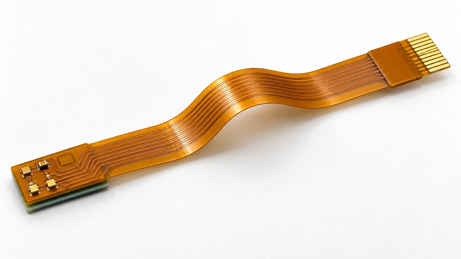
Figure: Polyimide flexible PCB with a PI stiffener
This guide will help you know how to select between adhesiveless and adhesive-based flexible copper-clad laminates (FCCL), understand the eight key steps in FCCL fabrication and how they differ in each board construction, determine appropriate film thicknesses and copper types, manage moisture and dimensional change for improved yield and reliability, and specify IPC requirements and prepare design files for FCCL fabrication.
What Is Polyimide Flexible PCB Fabrication?
Polyimide flexible PCB fabrication is the process used to build copper circuits on polyimide (PI) film, with imaging done on the copper, holes formed and plated, bonding of the PI coverlay over the circuit, finishing, testing, and cutting of the board while taking control of the moisture uptake and dimensional movement of the film.
The base material is a flexible copper-clad laminate (FCCL) copper foil/PI film (adhesive or adhesive-free). IPC-4204 covers these laminates, and coverlay films are covered by IPC-4203.
How Polyimide Works as a Flexible PCB Substrate
Copper conductors are insulated with polyimide, and each bend mechanically strains the polyimide. It is the most frequently used flex-circuit dielectric because it is flexible and has an adequate thermal resistance for lead-free soldering. The value of the property is dependent on the type of construction. These are the typical values mentioned in the data sheet EI-10124 provided by the DuPont Pyralux AP9121 adhesiveless laminate (50 µm PI, 35 µm copper):
- Dielectric constant: 3.4 at 1 MHz and 3.2 at 10 GHz
- Loss tangent: 0.002 at 1 MHz and 0.003 at 10 GHz
- Moisture absorption: 0.8% per IPC-TM-650 2.6.2
- Solder float: pass at 288 °C for 10 s per IPC-TM-650 2.4.13
- Glass transition temperature: 220 °C by TMA
Other PI laminate lists different values; design according to the data sheet for the laminate you specify. Consider three thermal ratings separately:
- Film thermal resistance: Property of the film per se, e.g., its glass transition behavior.
- Continuous operating rating: a rating of the complete construction, including adhesives, coverlay, and stiffener tapes that may restrict the capability of the film.
- Assembly reflow limit: The maximum temperature and time that the assembled board, finish, and components will withstand.
Polyimide Flex PCB Constructions and Applications
Polyimide FPCs are manufactured as single-sided, double-sided, or multilayer circuits. A flex board with stiffeners is still a flex board, since the stiffeners are non-electrical supports bonded locally. A rigid-flex board is a rigid laminate board with copper layers interlinked by plated holes.
The application sets the reliability requirement:
- Wearables and foldables: repeated dynamic bending – flex life governs the stackup.
- Medical sensors: thin, conformable circuits (material traceability).
- Aerospace electronics: thermal cycling and vibration, typically to Class 3.
- Industrial interconnects: static installation, bends with connector stiffeners.
Polyimide Flexible PCB Materials and Stackup Selection
Most of the performance of a polyimide flex PCB is determined by material selection before fabrication. The four decisions include laminate construction, film thickness, copper thickness, and the protective and support materials. The flex PCB stackup design guide takes an in-depth look at the layer structure.
Adhesiveless vs. Adhesive-Based Flexible Copper-Clad Laminates
Adhesiveless FCCL involves the direct bonding of copper to polyimide, whereas adhesive FCCL uses an acrylic (or epoxy) adhesive in between. The thickness and material properties of the adhesive have different thermal and mechanical properties from PI. Laminate construction is described by the terms "2-layer FCCL" or "3-layer FCCL", which refer to copper and PI, or to copper, adhesive, and PI. They are not used for indicating the number of copper layers in the completed PCB.
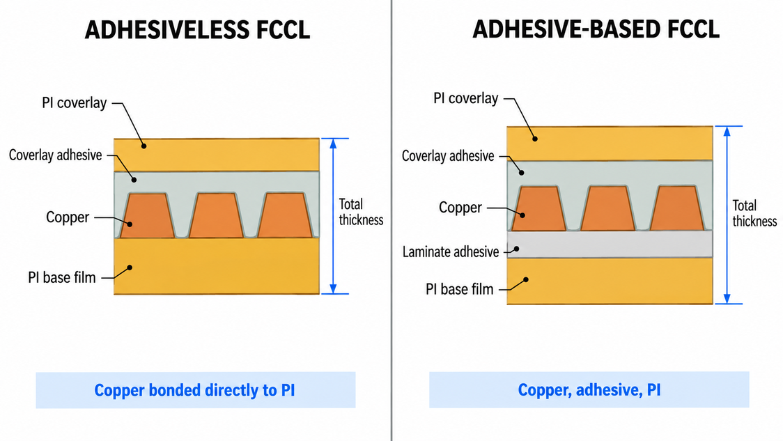
Figure: Polyimide FCCL cross-sections comparing adhesiveless copper-on-PI with copper
| Factor | Adhesiveless FCCL | Adhesive-Based FCCL |
| Construction | Copper bonded directly to PI | Copper, acrylic, or epoxy adhesive, PI |
| Thickness | Thinner for the same PI and copper | Adds the adhesive layer |
| Dimensional stability | Generally better | Adhesive can add movement during heating |
| Thermal cycling | Potential advantage, depending on the complete construction | Adhesive expansion can stress plated holes |
| Flex life | Preferred for dynamic bending | Suited to static and installation bends |
| Cost | Generally higher | Generally lower |
| Typical use | Fine-line, multilayer, dynamic flex | Cost-sensitive static flex |
Polyimide Film Thickness, Copper Weight, and Dielectric Properties
Thinner PI and thinner copper lead to a lower strain in the copper at a specified bend radius, which increases the flex life. The thicker the copper, the more current it will carry, although this will increase the finished thickness, the bend radius, and the minimum trace and space.
JLCPCB provides cores with thicknesses of 25 µm and 50 µm, and offers 12 µm / 18 µm / 35 µm copper on 2-layer and 4-layer boards. Laminate suppliers have a larger selection; Pyralux AP lists dielectric thicknesses ranging from 12 µm to 150 µm. A thinner core also means higher capacitance between the traces and planes, so a thinner trace is required to maintain the same impedance. The greater the separation of the outer copper from the neutral axis of the strip, the less it can withstand bending.
Rolled-Annealed vs. Electrodeposited Copper for Polyimide Flex PCBs
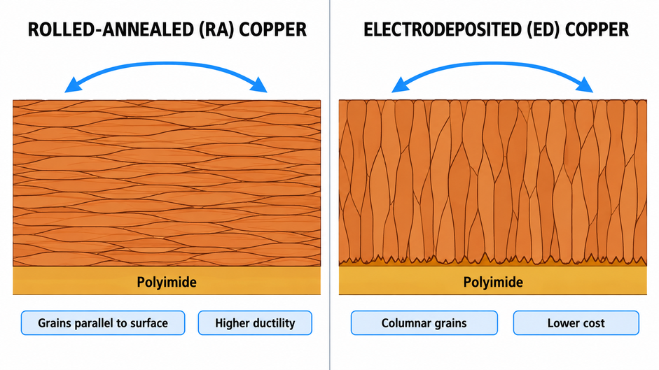
Figure: Rolled-annealed and electrodeposited copper grain structures
Rolled-annealed (RA) copper is rolled and annealed, resulting in elongated grains parallel to the foil surface. Electrodeposited (ED) copper is deposited onto a drum, resulting in a columnar grain structure. It is primarily due to that grain structure that RA copper is more resistant to fatigue from repeated bending.
| Property | RA Copper | ED Copper |
| Grain structure | Elongated, parallel to the surface | Columnar, perpendicular to the surface |
| Ductility and fatigue resistance | Higher | Lower for standard grades |
| Cost | Higher | Lower |
| Installation-only bends | Suitable | Suitable |
| Repeated dynamic bends | Preferred | Only grades qualified for flexing |
The grain structure of electroplated copper is similar to that of ED foil, and it is added to the surface by through-hole plating. IPC-2223, therefore, addresses the trade-offs among panel, pattern, and button plating: button plating is plating limited to hole pads and outside the bend.
Polyimide Coverlay, Stiffeners, and Surface Finishes
Coverlay is a PI film with an adhesive layer that is laminated onto the circuit under heat and pressure. It replaces the rigid-board Liquid Photoimageable (LIQUID SOLDERMASK). Coverlay openings are larger than solder mask openings and are cut before lamination, requiring clearance through which the adhesive can flow.
Stiffeners provide extra rigidity where the board needs to remain flat:
- PI stiffeners: set the contact thickness of ZIF connector tails to the connector specification.
- FR4 stiffeners: support connectors and component areas that need a stiff mounting surface.
- Stainless-steel stiffeners provide high stiffness in thin sections but are slightly magnetic.
Both are industry finishes for polyimide FPCs, with the addition of palladium for gold wire bonding in the case of ENEPIG. Avoid placing completed pads in bend areas, as nickel is less ductile than copper. JLCPCB documents ENIG for its flex boards. Refer to the JLCPCB coverlay article and the PCB stiffeners guide for more information.
Step-by-Step Polyimide Flexible PCB Fabrication Process
There are seven steps to making a polyimide flexible PCB: preparing a laminate PCB panel, imaging, hole formation, plating, coverlay bonding, finishing, profiling, and testing. The order will be based on the construction as shown below:
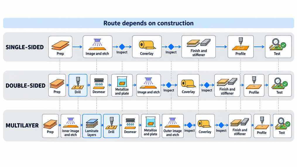
Figure: Polyimide flexible PCB single-sided, double-sided, and multilayer constructions
- Single-sided: imaging and etching, then coverlay; no plated holes.
- Double-sided: drilling and metallization usually come before outer-layer imaging.
- Multilayer: inner layers are imaged and etched, laminated together, then drilled and plated.
The JLCPCB flex PCB manufacturing process overview describes the general flow for all flex materials.
Step 1: Design Review, Material Preparation, and Preconditioning
Fabrication includes a design-for-manufacturing (DFM) check to verify the Gerber, drill, outline, stiffener, and coverlay data against the limits for trace, space, annular ring, and coverlay clearances. The laminate then undergoes inspection, is cut into panels, and has tooling holes added. If the laminate supplier or process requires it, panels can be baked to control moisture levels before imaging.
Step 2: Photoimaging, Circuit Patterning, and Copper Etching
The copper is cleaned and micro-etched; a dry-film photoresist is laminated on, exposed, and developed. Un-etched copper is removed after developing, and the resist is stripped.
The thicker the copper, the more undercutting there will be because etching removes the copper not only downward but also sideways. As mentioned before, the artwork traces are widened by CAM to compensate, hence the increase in minimum trace and space with copper weight. Thin panels also require carriers or frames to keep them flat along conveyorized lines.
Step 3: Mechanical Drilling, UV Laser Drilling, and Desmear
Holes that pass completely through the panel are frequently mechanically drilled in stacked panels that have entry and backup sheets. If bits are worn or there is not enough bit stack, it can lead to burrs and adhesive smearing on the copper inside the hole. Laser drilling is one option, but not a requirement. Both copper and polyimide are ablatable with UV lasers, thus making them suitable for small-hole and blind microvia applications. Next, holes are desmear, usually with plasma, and some adhesiveless laminates, including Pyralux AP, are specified by their manufacturers as desmearable.
Step 4: Electroless Copper Deposition and Electroplating
Electroless Copper—Also referred to as Direct Metallization, a process that builds thin layers of conductive material on the non-conductive walls of holes. Then the copper barrel is electroplated to the desired thickness. The barrel's ability to withstand thermal stress during assembly depends on the plating's uniformity and adhesion. Micro-etching, etc., is not metalizing the hole; it's preparing the separated copper.
Step 5: Multilayer Alignment and Lamination
Multilayer boards consist of a stack of inner plates with images on them, which are stacked on pins or optically and then joined together with controlled heat, pressure, and vacuum. Voids and delamination are due to misregistration, trapped moisture, and improper lamination conditions. Single-sided and double-sided boards do not perform this lamination step; their primary lamination step is coverlay bonding.
Step 6: Polyimide Coverlay Alignment and Bonding
Coverlay openings are drilled, punched, or laser-cut before installing. It is coverlaid, tacked, laminated, and cured in a vacuum-assisted coverlay press to line up with the pads. Common failure modes are:
- Bubbles or voids: Air and/or moisture between the coverlay and circuit.
- Misalignment: an open that reveals a trace or part of a pad.
- Adhesive squeeze-out: adhesive coming out onto a pad, reducing the solderable area.
Step 7: Stiffener Attachment, Surface Finishing, and Profiling
Exposed copper is surface-finished with ENIG, and stiffeners are made of PI, FR4, or stainless steel and are bonded using a thermosetting adhesive or pressure-sensitive tape. Laser or die punching is used to cut out the outline. Laser cutting requires no hard tooling and is ideal for prototypes; die punching is ideal for high volume. Both affect the edge quality; therefore, profiler tolerance and the distance between the copper and the edge are adjusted simultaneously.
Step 8: Electrical Testing, Inspection, and Packaging
Each board is subjected to opens and shorts testing, optically inspected for coverlay and etch defects, and measured to the outline drawing. Bend checks are added when they come up in the fabrication documentation. Packaging for finished FPCs is typically moisture-barrier with or without desiccant to be assembled flat and minimize moisture pick-up.
Engineering Challenges in Polyimide Flexible PCB Fabrication
The key engineering issues for polyimide flexible PCB manufacture are moisture uptake, dimensional movement, bending-induced strain, and stress concentration at the transitions. All of them are determined both by the fabricator and the layout.
Moisture Absorption, Pre-Baking, and Reflow Reliability
Polyimide will absorb moisture from the air. Water absorbed by the board will vaporize during reflow, resulting in blistering, overlay lift, or delamination, particularly in adhesive constructions and under large copper areas.
Moisture control is a combination of storage and baking:
- Store FPCs in sealed moisture-barrier packaging until assembly.
- Bake before reflow when exposure time or the supplier's instructions require it.
- Assemble within the time window that follows baking.
“There's no such thing as a universal baking recipe.” Depending on the laminate, moisture absorption, surface finish, stiffener adhesive, and the supplier's instructions, IPC-1602 establishes handling and storage requirements for printed boards.
Minimum Bend Radius, Neutral Axis, and Static vs. Dynamic Flexing
Minimum bend radius is calculated from the finished thickness of the flex section:
R_min = k × t
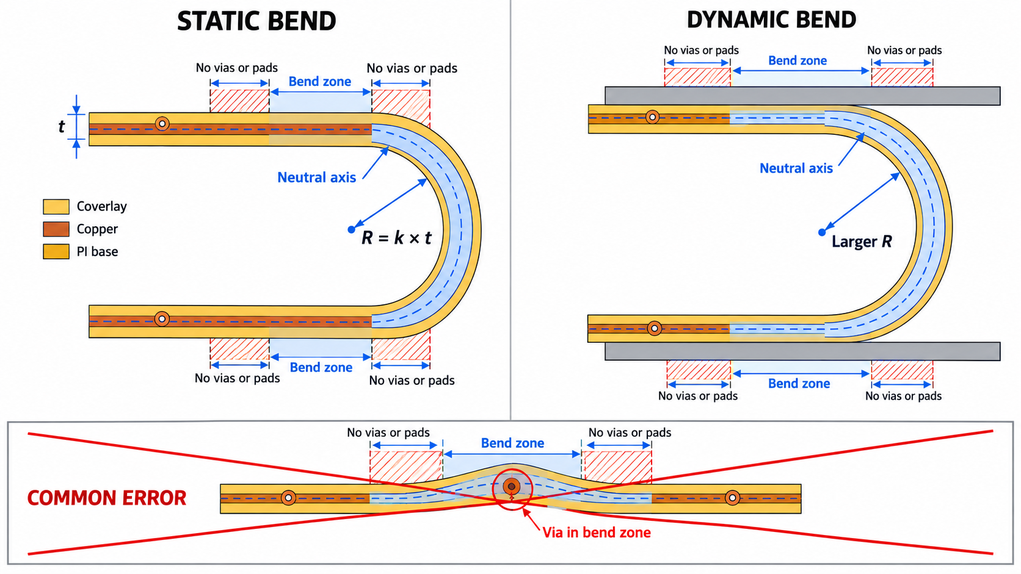
Figure: Static and dynamic polyimide flex bends showing the neutral axis
Here, t is the finished flex thickness, including coverlay and adhesives but excluding stiffeners, and k is an application-dependent multiplier. The radius is measured at the inside surface of the bend.
| Factor | Static Bend | Dynamic Bend |
| Definition | Bent once or a few times during installation | Bent repeatedly in service |
| Minimum multiplier k (JLCPCB capability page) | ≥6× single-layer, ≥10× multilayer | ≥10–15× |
| Conservative multiplier k (JLCPCB bend radius guide) | 6× single-layer, 12× multilayer | 100× single-layer, 100–150× multilayer |
| Preferred construction | 1–4 layers | 1–2 layers, adhesiveless PI |
| Copper | RA or ED | RA or a flex-rated grade |
| Vias and pads in a bend | Avoid where possible | Keep out of the bend zone |
Worked example: Assume a JLCPCB 2-layer board on 25 µm PI with a finished thickness of 0.12 mm, folded once into an enclosure. With k = 10 for a multilayer static bend, R_min = 10 × 0.12 mm = 1.2 mm. If the same section must flex repeatedly at k = 100, R_min = 12 mm.
Quality Verification and IPC Standards for Polyimide Flex PCBs
Quality verification ensures that a polyimide flex PCB operates at the performance class specified in the PCB fabrication documentation. The design requirements are specified in IPC-2223; the class is specified in the procurement documents; and the qualification and performance requirements are specified in IPC-6013.
IPC-6013 and IPC-2223 Design and Performance Requirements
IPC-2223 is a sectional design standard for flexible and rigid-flexible printed boards, in conjunction with the base standard, IPC-2221. The qualification and performance specification for the same boards is IPC-6013. Both of these standards are at Revision F (IPC-2223F and IPC-6013F); therefore, indicate the revision on the fabrication drawing.
The second way that IPC-6013 classifies boards is by construction type, ranging from Type 1 single-sided flex to Type 4 rigid-flex multilayer, and Type 5 for boards with 2 or more conductive layers, but no plated through-holes. Performance class is not included. Class 2 applies to the dedicated-service electronics, and Class 3 applies to high-reliability products.
Cross-Section Inspection, Peel Strength, and Bending Endurance
Three tests ensure that properties that are not visible to the naked eye are verified:
- Cross-section (microsection) IPC-TM-650 2.1.1: Test plating thickness, barrel cracks, voids, smear, and layer registration.
- Peel strength: IPC-TM-650 2.4.9: Copper Adhesion to Dielectric, as received and after solder.
- Flexural endurance (IPC-TM-650 2.4.3): Conducts a conductor pattern at a specified radius and counts the number of cycles until it breaks, indicating fatigue performance of dynamic designs.
Common Manufacturing Defects and Acceptance Criteria
Acceptance limits are specified in IPC-6013 for the specified class and in the procurement documents. These defects are most often traced to polyimide behavior:
| Defect | Likely Cause | How It Is Detected | Controlling Stage |
| Coverlay bubbles | Trapped air or moisture during bonding | Visual and optical inspection | Step 6: Coverlay lamination |
| Copper trace cracking | Excessive bending strain or fatigue | Continuity test, flex testing, microsection | Design, copper selection |
| Pad misregistration | Film movement or alignment error | Optical inspection, dimensional check | Steps 1 and 6, CAM scaling |
| Barrel cracking | Thin plating or thermal and mechanical stress | Microsection, thermal stress test | Steps 3 and 4 |
| Delamination | Weak bonding, moisture, or contamination | Visual inspection after thermal stress | Steps 5 and 6, moisture control |
JLCPCB Polyimide Flexible PCB Manufacturing Capabilities
JLCPCB can manufacture 1-layer, 2-layer, and 4-layer polyimide flex PCBs, but cannot supply rigid-flex boards. These values are from the JLCPCB flex PCB capabilities page; the difference between regular and extreme limits may be that the extreme limits may be subject to extra charges and/or confirmation.
JLCPCB Layer Counts, Stackups, Trace/Space Limits, and Via Capabilities
| Parameter | Published Capability |
| Copper layers | 1, 2, and 4 |
| PI dielectric | 25 µm or 50 µm; adhesive and adhesiveless PI |
| Copper thickness | 12, 18, or 35 µm (12 µm on 2-layer and 4-layer only) |
| Minimum trace/space, regular | 3/3 mil (12 µm), 3.5/3.5 mil (18 µm), 4/4 mil (35 µm) |
| Minimum trace/space, extreme | 2/2 mil on 12 µm copper |
| Via hole/pad, regular | 0.3 mm / 0.55 mm |
| Via hole/pad, extreme | 0.10/0.30 mm (2-layer), 0.15/0.35 mm (4-layer), extra cost |
| Coverlay colors | Yellow, black, white, transparent |
| Stiffeners | PI, FR4, stainless steel |
| Surface finish | ENIG |
| Outline | Laser cut, ±0.1 mm |
| Maximum board size | 234 × 490 mm regular |
The via values are finished hole and pad diameters, not laser-microvia positional tolerances.
Preparing Gerber Files, Stiffener Drawings, and DFM Documentation
JLCPCB's Gerber file preparation guide states that flex Gerber files are essentially the same as FR4 files, except for an additional layer indicating the stiffener position and thickness. Coverlay openings are defined on the solder mask layers. A complete flex data package includes:
- Copper, solder mask (coverlay), and silkscreen layers
- Drill file and board outline
- A stiffener layer showing outline, material, and thickness
- Bend regions and stackup notes on a documentation layer
EasyEDA has a special stiffener layer. For other EDA tools, please place each type and side of stiffeners on their respective layers named with JLCPCB's prefix and thickness, such as pit_0.25 for a top PI stiffener with 0.25mm thickness, gpb_0.2 for a bottom steel stiffener with 0.2mm thickness, as shown in the FPC stiffener guide. Next, choose the appropriate stiffener material and thickness in the order form.
From Prototype to Production: Online Quotation and Turnaround
When the Gerber files are uploaded to JLCPCB's online quote page, the quotation and DFM pages will be generated. Lead time will vary with the number of layers, quantity, stiffeners, extreme-limit features, and any engineering questions raised during review. The notes are clear, and the stiffener, stackup, and bend-region notes are minimized, thereby eliminating the need for clarification rounds. The same things apply to price – the number of layers, laminate type, and feature complexity.
Conclusion
The use of a polyimide flexible PCB, sound material selection, process control, and layout make for sound design choices, and the introduction is successful. Indicate laminate construction, copper type, number of layers, moisture handling, and IPC class in the fabrication documents and verify the bend radius in the actual construction. This ensures registration, reflow yield, and flex life remain predictable from prototype to production. Once your files are all prepared, test them for capability and upload your design to get a flex PCB quote.

FAQs About Polyimide Flexible PCB Fabrication
Q. Why Is Adhesiveless Polyimide Preferred for High-Density Flexible PCBs?
Ans: Adhesiveless polyimide eliminates the adhesive layer, making the laminate thinner and generally more dimensionally stable. That supports finer lines, tighter registration, and smaller bend radii. It can also improve the thermal cycling reliability of plated holes, depending on the overall construction.
Q. How Does Moisture Absorption Affect Polyimide PCB Fabrication During SMT Reflow?
Ans: Moisture absorbed by the polyimide and adhesives vaporizes at reflow temperature, and the vapor pressure can cause blistering, coverlay lift, or delamination. Sealed storage and baking in accordance with the laminate or board supplier's instructions reduces that risk.
Q. What Is the Typical Bend Radius for a Double-Sided Polyimide Flexible PCB?
Ans: At least 10 times the finished flex thickness for a static bend, so a 0.12 mm double-sided board needs at least 1.2 mm. Dynamic bends require a minimum of 10–15 times, and up to 100–150 times for high cycle counts.
Q. Can Polyimide Flexible PCBs Withstand Direct SMT Reflow Soldering?
Ans: Yes. Polyimide FPCs are commonly reflow-soldered with lead-free profiles when the laminate, coverlay adhesive, and stiffener tape are rated for it. Moisture control is required, and stiffener tapes must be heat-resistant; JLCPCB lists 3M468 tape as not heat-resistant.

Keep Learning
Best Flex PCB Design Software: CAD Tools & Setup Guide
The right flex PCB design software would rely on the complexity and construction of your circuit. Altium Designer, Cadence Allegro X, OrCAD X, and Siemens Xpedition are professional tools that offer advanced capabilities for flexible and rigid-flex PCB designs, such as stackup management, bend regions, and mechanical constraints. In the meantime, for more basic flexible circuits, tools such as KiCad or EasyEDA Pro might be viable options, though they may require some manual setup and verification. Fle......
Custom FPC Fabrication: Design Rules & Manufacturing Guide
Custom FPC fabrication is the process of making flexible printed circuits in accordance with a customer's design requirements, such as board outline, layer stackup, copper thickness, openings for coverlay, and stiffener placement. Custom flexible circuits differ from traditional rigid PCBs in that they must be carefully designed and planned for materials and layout to meet flexibility and stress requirements and to fit into smaller assemblies. These design decisions are directly related to manufactura......
Polyimide Flexible PCB Fabrication: Materials and Process Guide
Polyimide flexible PCB fabrication is a process of creating thin polyimide film and copper-foil-based circuits that will bend, fold, and withstand soldering temperatures. But the same flexibility that comes from the thin film material used on these boards, and which is sensitive to moisture, makes production slightly more difficult than rigid PCBs. Polyimide can expand or contract during processing, absorb moisture before reflow soldering, and suffer from copper fatigue or cracking if the bend radius ......
Flexible PCB Price: Key Cost Factors and Ways to Save
The price of a flexible PCB has no single fixed figure, as it depends mainly on the panel area occupied by the design, the number of copper layers, and the order quantity. Other features such as stiffeners, EMI shielding film, tight outline tolerance, and a complex via structure may further increase manufacturing costs. The majority of these cost factors are fixed by the PCB layout stage, and even at the time of the first quotation. Figure: Polyimide flexible PCB with ENIG contact pads and a bonded st......
Flex PCB Design Guide: Preventing Mechanical Failures
Key Takeaways Reliable flex PCB design requires more than electrical performance. Proper bend radius control, trace routing, via placement, stiffener selection, and DFM considerations are essential to prevent mechanical failures such as copper cracking and delamination. By following proven flexible PCB design practices, engineers can improve durability and achieve reliable production results with JLCPCB. Ever wonder how the circuit in a foldable phone, fitness tracker, or camera module manages to rema......
FPC Electronics: What Is It, How It Works, Applications, and Benefits
FPC electronics is the reason your phone camera still works after a hundred open-and-close cycles. Peel apart almost any modern device, and you will find a thin amber ribbon carrying signals around corners no rigid board could turn. In this guide, you will learn: What does FPC stand for, and what are the differences between FFC and FPC? A flexible circuit that conducts a signal as it flexes The materials include one polyimide, copper, coverlay, and stiffener FPC manufacturing process (etching to elect......