
Flex PCB Stackup Design Guide: Layers, Materials & Reliability
12 min
- Understanding Flex PCB Stackup Structures
- Core Materials Used in Flex PCB Stackups
- Key Design Considerations for Flex PCB Stackup
- Electrical and Mechanical Reliability Considerations in Flex PCB Stackups
- Manufacturing and DFM Considerations for Flex PCB Stackups
- JLCPCB's Flexible PCB Stackup and Manufacturing Capabilities
- Frequently Asked Questions (FAQ)
Key Takeaways
A reliable flex PCB starts with the right stackup design. The layer structure, material selection, and copper arrangement directly affect flexibility, bend life, electrical performance, and manufacturing reliability. This guide explains single-sided, double-sided, and multilayer flex PCB stackups, including polyimide materials, coverlay, copper types, and key design considerations for creating durable flexible circuits with JLCPCB.
Did you ever wonder how a foldable phone can last for 200,000 bend cycles without a cracked trace? There is no magic; itis a well-designed flex PCB stackup. How you layer polyimide, copper, and coverlay determines if your board is going to bend nicely or not bend at all. Today, flex circuits can be found in wearables, camera modules, automotive sensors, medical probes, and so many other applications. However, unlike rigid boards, a flexible PCB stackup must be designed to meet two somewhat conflicting requirements: electrical performance and mechanical durability.
The layer structure is important because if this is incorrect, copper fatigue or delamination, or impedance drift is observed well before the end of life. Here, we will discuss flex PCB layer structures from single-sided to multi-layer and the core materials used to enable them. At the end, you'll be equipped to know exactly how to create a stackup that will bend but not break.
Understanding Flex PCB Stackup Structures
The vertical structure of all conductive and dielectric layers that make up a flex PCB is called a flex PCB stackup. The base is almost invariably polyimide, and copper foil is affixed to one or both sides, which are then covered with a coverlay to protect the conductors. Since the substrate is very thin and flexible, each layer added alters the electrical characteristics as well as the flex properties. The basic flex design guideline is that the fewer the layers, the easier it is to bend. A single-sided flex can be bent around a small radius without any problem; a six-layer stack is virtually like a rigid board. The right structure is selected to match the number of flex requirements, rather than the number of routing requirements, for the application.
Single-Sided, Double-Sided, and Multilayer Flexible PCB Layer Structures
Flex circuits are divided into 3 major categories, which are based on conductor layers. As the complexity increases, so does the routing capacity at the expense of flexibility.
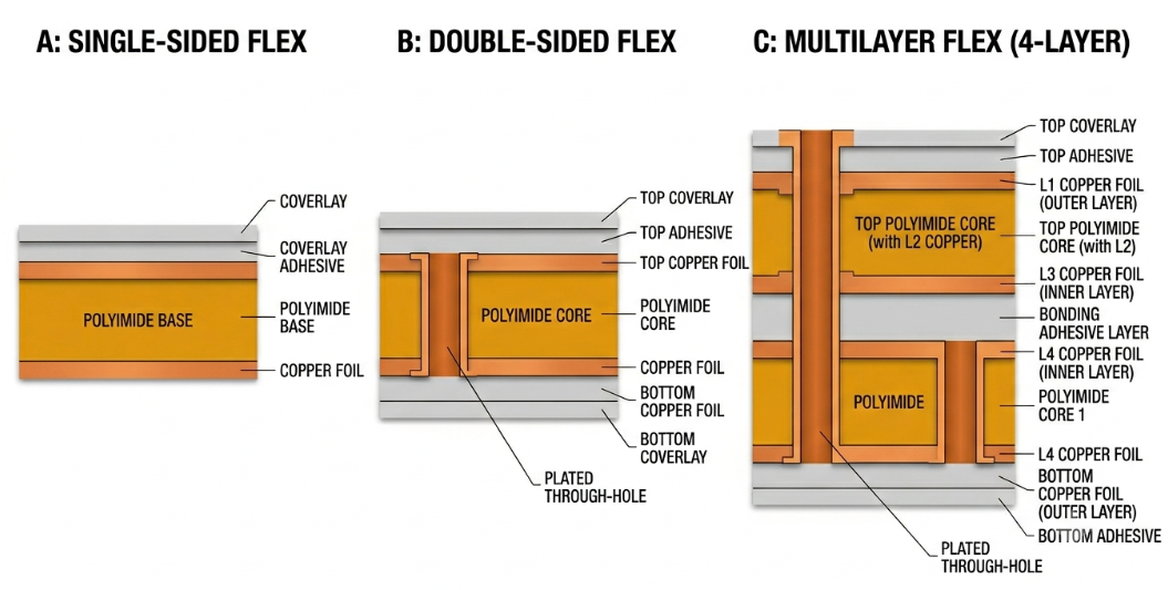
- Single-sided flex: One copper layer on top of a polyimide base, which is covered by one coverlay. This is the most adaptable and least expensive choice, suitable for movable bending parts, such as printer heads and hinges.
- Double-sided flex: Copper on both sides of polyimide core (plated through-holes). It offers crossover routing and simple impedance control and is moderately flexible.
- Multilayer flex: Three or more layers of copper with adhesive or bond ply. These are for high-speed routing and are very dense, but are only used in static or low-flexible areas.
How Stackup Structure Affects Flexibility and Reliability
The bending stress during flexing is a direct result of the number and location of the copper. The flex circuit outer surface is placed in tension, and the inner surface in compression. Copper furthest away from the central position will be under the greatest strain, and it will be more prone to fatigue cracking. Hence, the single-sided designs have the longest life in dynamic applications. The single copper layer can be located close to the neutral axis, the zero-strain plane of the bend. With each layer, the copper tends to move away from this plane, and reliability during repeated flexing decreases significantly. Thus, symmetry and thin dielectrics are important considerations to maintain controllable stress.
Core Materials Used in Flex PCB Stackups
The greatest difference between flex design and rigid FR4 work is in the materials. All flexible PCB stackup layers should be able to withstand bending, thermal cycling, and lamination without cracking or delamination. These three components are the dielectric film, copper foil, and coverlay.
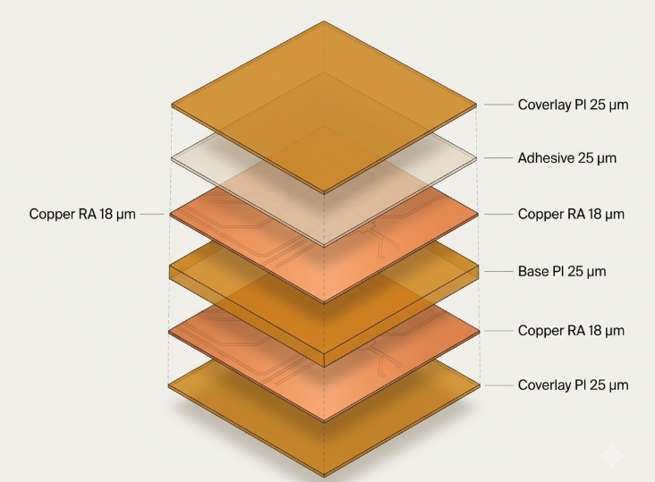
Polyimide, Copper Foil, and Coverlay Materials
The most popular dielectric used in flex circuits is polyimide (PI) because it has excellent thermal stability (200°C or more), low moisture absorption, and excellent flexing characteristics. Typical thicknesses of base film range from 12.5 µm to 50 µm (½ mil to 2 mil), with the thinner film providing a smaller bend radius. The dielectric is not the only choice that is significant, but so is the copper foil too. Two grades dominate:
- Electrodeposited (ED) Copper: Less expensive, but has a columnar grain structure. It is suitable for static flex, but it is quicker to become fatigued when flexing repeatedly.
- Rolled annealed (RA) copper: A structure with horizontal grain that is resistant to crack propagation. The standard choice of RA copper for dynamic flex and applications with a high number of cycles.
The coverlay takes the place of the solder mask that is applied to rigid boards. It is usually a film of polyimide with a glue layer laminated over the conductors, which provides insulation and mechanical protection. It is also possible to use a photoimageable coverlay (same as LPI solder mask), but in flexing areas, film coverlay is still more durable.
Adhesive-Based vs Adhesiveless Flex PCB Structures
Flex laminates are available in two families of construction, which can make a big difference in reliability. There are two types of laminate: adhesive-based, in which copper is bonded to the polyimide with an acrylic or epoxy adhesive; and adhesiveless, in which the copper is deposited directly on the polyimide. Adhesiveless construction is more desirable for high reliability and high-density designs. The loss of acrylic adhesive, which has a high coefficient of thermal expansion, will help minimize the risk of barrel cracking of plated through-holes during thermal cycling and during assembly reflow.
Key Design Considerations for Flex PCB Stackup
Bend Radius Guidelines and Neutral Axis Design
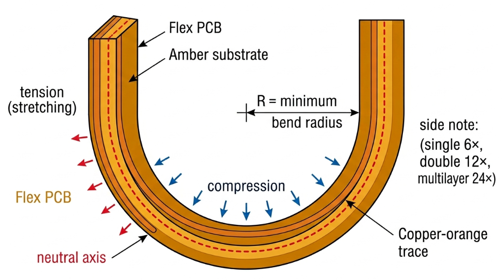
Bend Radius is the smallest radius that the flex circuit can be bent to without damaging the copper. It is given as a multiple of the total flex thickness; the rules are tighter as the number of layers increases. The following minimums are recommended in accordance with industry guidelines, which are also based on IPC-2223 (sectional design standard for flex):
| Construction | Minimum Bend Radius (static) | Minimum Bend Radius (dynamic) |
|---|---|---|
| Single-sided | 6× thickness | 20–40× thickness |
| Double-sided | 12× thickness | 40–100× thickness |
| Multilayer | 24× thickness | Not recommended |
Neutral axis design is to place the most strain-sensitive copper as near to the center of the bend as possible. Single-sided flex allows the thickness of coverlay and base to be varied to position the copper near the neutral axis. Staggering the top and bottom traces in double-sided dynamic flex decreases the total stiffness in the bending area.
Copper Balancing and Mechanical Stress Control
Copper balancing is the process of ensuring that copper is distributed evenly, layer to layer, and across the board area. The nonuniform distribution of the Cu results in warping of the laminate during lamination, and also results in the concentration of mechanical stress at the boundaries between the heavy and light Cu. Here are some tips for controlling stress:
- Routes parallel to the bend line are never used; the bend is used to stretch the dielectric and not the conductor edges.
- Stay clear of plated through-holes, pads, and vias within any bend area; they are stress risers and crack initiation sites.
- Avoid square 90° corners that focus strain by using curved traces and teardrop pad transitions.
- Consider using a small copper fillet or “rabbit-ear” anchor at the pad to trace connections to prevent peeling.
Electrical and Mechanical Reliability Considerations in Flex PCB Stackups
Impedance Control and Crosstalk Considerations
However, controlled impedance on flex is more challenging than FR4, because the dielectric constant (Dk) of polyimide is different (Dk≈3.2-3.5), and the thickness of dielectrics is very small. A continuous reference plane is not needed to achieve a 50 Ω single-ended or 100 Ω differential target; often, wider traces or a coplanar ground structure are sufficient. A flex design usually uses a cross-hatched (mesh) ground plane, since solid copper reference planes are a hindrance to flexibility. The hatch pattern helps to maintain bendability and offers a path for return, albeit with an increased impedance, which needs to be modeled. These are the rules of crosstalk and impedance to keep in mind:
- Use the same spacing for traces to planes throughout the signal path to prevent impedance discontinuities.
- Use the 3W rule when routing in parallel for sensitive applications (three trace widths from center to center).
- Make sure to account for the cross-hatch fill percentage in the effective Dk and Impedance calculations.
Thermal Stability and Dynamic Flex Reliability
Due to polyimide's high glass transition temperature (Tg), flex circuits have a large thermal headroom, but the stackup still must pass reflow and field thermal cycling. Plated through holes are the most common cause of failure due to CTE mismatch between copper, adhesive, and polyimide. So, for thermally demanding designs, only adhesiveless construction is preferred.
For dynamic applications, reliability is measured in flex cycles. Rolled annealed copper, copper near the neutral axis, and consideration of dynamic bend radius can extend cycle life to hundreds of thousands or millions of bends. Always check with bend-cycle testing before going to volume production. Simulation only provides a prediction of trends; actual fatigue behavior is dependent on the quality of the lamination.
Manufacturing and DFM Considerations for Flex PCB Stackups
Lamination Accuracy and Layer Alignment Challenges
Unlike FR4, polyimide films tend to shrink and expand during processing, making the registration of the layers the most difficult aspect of multilayer flex fabrication. During film etching, baking, and lamination, the film layers may move by tens of microns across a panel, changing the alignment of the layers. Fabricators take care with scaling factors and relaxed annular ring allowance; designers take care not to make the features as dense as possible. Another key step is coverlay registration, where openings must match up with pads, and an excessive amount of glue on the edges might be squeezed out into bend areas and cause the circuit to stiffen in unexpected ways.
DFM Checks for Reliable Flexible PCB Production
The most frequent flex failures can be avoided by a thorough DFM review prior to release. Prioritize these checks:
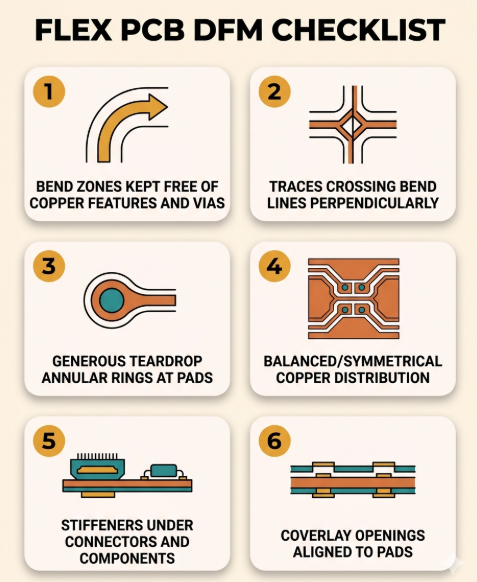
- Bend zones have no copper features (no vias, pads, or stiffeners in any flexing area).
- Traces perpendicular to bend lines and utilizes curved geometry rather than sharp angles.
- Plated through-holes are generous because of their annular rings to take up registration shift.
- Copper is balanced both layer-to-layer and across the panel to minimize warpage.
The earlier these things are caught, the less cost is involved in them. A clean DFM package also reduces the back and forth with your fabricator, and puts boards into production sooner.
JLCPCB's Flexible PCB Stackup and Manufacturing Capabilities
Flexible PCB Material and Stackup Options
The flex product offering from JLCPCB is based on polyimide base material, which is available in single-sided, double-sided, and multilayer constructions. Designers can specify copper weights appropriate for their bending and current-carrying needs, coverlay protection, and optional stiffening beneath connector and component areas.
For controlled-impedance designs, the published stackup information allows the modeling of trace geometry on the polyimide dielectric prior to fabrication. This, together with EasyEDA integration and an instant quoting system, makes it easy to make iterations on a flexible PCB stackup without any guesswork. With a quick turnaround from upload to production, flex prototypes can be as tight as development cycles are.
Reliability-Focused Fabrication and Quality Inspection
Reliability in flex depends on the fabrication discipline, and quality check is a built-in process. Boards are sent through automated optical inspection (AOI) to ensure trace integrity and coverlay registration, followed by electrical testing, which ensures continuity and isolation before they are shipped. When it comes to implementing stackup and reliability principles, JLCPCB's flex PCB service allows for easy material specifications, stiffener requests, and prototyping your design in smaller quantities. That allows you to test the performance of bends and the impedance characteristics on actual hardware before placing an order.

Frequently Asked Questions (FAQ)
Q: What is the most flexible flex PCB stackup structure?
Ans: Single-sided flex is the most flexible because it has only one copper layer that can sit near the neutral axis. It is the preferred choice for dynamic bending applications like hinges and actuators.
Q: Why is rolled annealed copper preferred for dynamic flex?
Ans: Rolled annealed (RA) copper has a horizontal grain structure that resists crack propagation under repeated bending. This gives it far better fatigue life than electrodeposited copper in dynamic flex applications.
Q: What is the minimum bend radius for a flex PCB?
Ans: For static bending, single-sided flex typically allows 6× the total thickness, while double-sided needs about 12×. Dynamic applications require much larger radii, often 20–100× thickness,s depending on layer count.
Q: Why use a cross-hatched ground plane in flex designs?
Ans: A solid copper plane stiffens the circuit and reduces flexibility, so a cross-hatched mesh plane preserves bendability while still providing a return path. The hatch pattern must be accounted for when calculating impedance.
Q: What is the difference between adhesive-based and adhesiveless flex?
Ans: Adhesive-based laminates bond copper to polyimide with an acrylic or epoxy adhesive, while adhesiveless laminates deposit copper directly onto the polyimide. Adhesiveless is thinner, more flexible, and more reliable under thermal cycling.

Popular Articles
• 45 Must-Know Flex PCB Design Tips You Can't Afford to Miss!
• Choosing the Right Bend Radius for Durable Flexible PCBs
• FPC Design Rules: 13 Safety Distances You Can’t Ignore
• Mastering PCB Stiffeners: A Comprehensive Guide to Types, Applications, and Design Best Practices for Flexible Circuits
• How Flex Coverlay Protects and Enhances Flexible PCB Durability
Keep Learning
Flex PCB Manufacturing Process: From Prototyping To Mass Production
Flexible Printed Circuit Board commonly known as flex PCBs are a revolutionary step in modern electronics that offer compact, lightweight, dynamic and precise designs. Flex PCBs are designed to bend, twist, and fold, which rigid boards are incapable of. These characteristics have led to their widespread adoption in industries like wearable technology to consumer electronics to aerospace and medical technologies. With demands increasing day by day for miniaturized and ergonomic product designs, underst......
45 Must-Know Flex PCB Design Tips You Can't Afford to Miss!
Achieving perfection in product design requires a careful balance between meeting design requirements and manufacturing standards. However, when it comes to flex PCB (FPC) design, many engineers find themselves at a loss, unsure of where to begin. In this insightful guide, we will delve into 45 essential design guidelines for FPC. By the end, you'll have the knowledge and confidence to navigate the complexities of flex PCB design. Outline and Drilling 1. The minimum distance from through-holes to the ......
Choosing the Right Bend Radius for Durable Flexible PCBs
Key Takeaways Mastering the bend radius is essential for reliable flexible PCB design. Following IPC-2223 guidelines, maintain a minimum of 6× total thickness for static bends and 100× for dynamic applications, while using thinner RA copper, adhesiveless polyimide, staggered traces, and cross-hatched patterns in flex zones. Proper material selection, layer stackup optimization, and adequate clearance from stiffeners can dramatically extend flex life and prevent premature trace cracking or delamination......
FPC Connector Guide: Types, Pitch & Reliability
Key Takeaways Choosing the right FPC connector is critical for reliable flexible electronic designs. Connector type, pitch, pin count, stiffener thickness, and PCB layout all affect signal integrity and mechanical durability. By understanding FPC connector selection and design considerations, engineers can reduce connection failures and achieve reliable assembly results with JLCPCB. As you know, the electronics world is getting smaller; nowadays, the devices need to be thin and light. All the parts sh......
Flex PCB Design Guide: Preventing Mechanical Failures
Key Takeaways Reliable flex PCB design requires more than electrical performance. Proper bend radius control, trace routing, via placement, stiffener selection, and DFM considerations are essential to prevent mechanical failures such as copper cracking and delamination. By following proven flexible PCB design practices, engineers can improve durability and achieve reliable production results with JLCPCB. Ever wonder how the circuit in a foldable phone, fitness tracker, or camera module manages to rema......
Flex PCB Prototyping Guide: Materials & Design Tips
Key Takeaways A reliable flex PCB prototype requires more than just a working circuit. Material selection, bend radius control, copper design, panelization, and stiffener choices directly impact flexibility, durability, and manufacturing success. By following proper flexible PCB prototyping practices, engineers can reduce design risks and smoothly transition from prototypes to production with JLCPCB. Ever wonder how the circuit in a smartwatch, a foldable phone, or a camera module can take the shape? ......