
FPC Stiffener Materials & EMI: Introduction, Ordering Options, and Layer Naming Guide
Last updated on Jun 18, 2026
FPC (flexible printed circuit) stiffener materials improve local mechanical strength and structural stability. They are mainly used in connector installation areas and other critical areas requiring support. Selecting an appropriate stiffener material is essential for ensuring FPC performance and reliability. Selection should be based on the specific application environment, mechanical strength requirements, and thermal performance.
Introduction to Stiffener Materials
The stiffener materials currently used by JLCPCB mainly include the following types:
1. PI Stiffener (Polyimide)
1.1 Characteristics:
- High-temperature resistance: PI offers excellent high-temperature resistance and is suitable for high-temperature soldering.
- Compatible flexibility: PI is highly compatible with FPC substrates, which are usually also made of PI, and retains some flexibility after stiffening.
- Chemical and corrosion resistance: PI resists chemicals and environmental corrosion, making it suitable for harsh operating conditions.
1.2 Applications
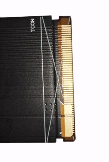
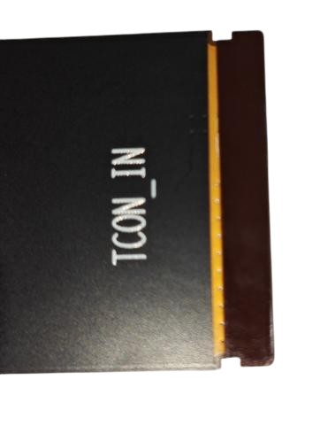
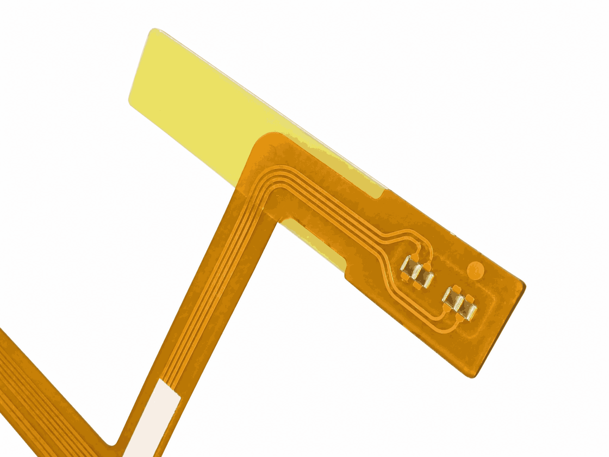
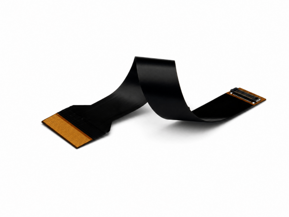
Typically used in electronic devices requiring high-temperature soldering and high reliability, such as the ZIF connector ends of mobile phone display FPCs and battery FPCs, especially at plug-in gold fingers, as shown below:
1.3 JLCPCB PI Stiffener Layer Naming Rules
| Type | Side | Specification | Naming Rule |
|---|---|---|---|
| PI Stiffener | Top | 0.1, 0.15, 0.2, 0.225, 0.25 mm | pit_* |
| PI Stiffener | Bottom | 0.1, 0.15, 0.2, 0.225, 0.25 mm | pib_* |
Example: a 0.25 mm PI stiffener on the top side can be named pit_0.25.
1.4 Ordering Options and Notes
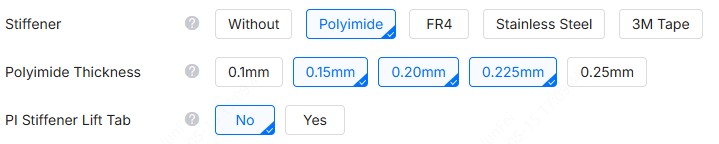
1.4.1 Select Polyimide in the Stiffener field, then select the polyimide thickness. Multiple thicknesses may be selected according to the actual stiffener requirements in the Gerber files.
1.4.2 Select the PI Stiffener Pull Tab option if any part of the PI stiffener extends beyond the board outline or does not adhere to the board, because additional processing is required.
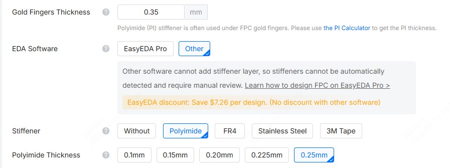
1.4.3 If gold fingers are selected, use the calculator to determine the PI thickness and select the corresponding thickness as shown below:
2. FR-4 Stiffener (Fiberglass Epoxy)
2.1 Characteristics
- High mechanical strength: FR-4 offers excellent mechanical strength and rigidity, providing strong local support.
- Rigid support: FR-4 is harder than flexible materials and is suitable for applications requiring rigid support.
- High-temperature resistance: FR-4 provides a degree of high-temperature resistance and can be used for conventional high-temperature soldering.
2.2 Applications
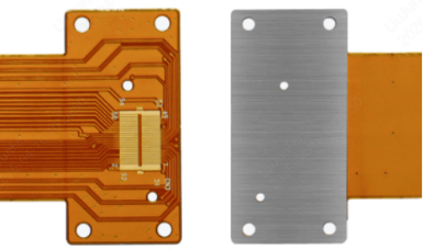
Generally used in areas with through holes or on the back of connectors where flatness requirements are not stringent.
2.3 JLCPCB FR4 Stiffener Layer Naming Rules
| Type | Side | Specification | Naming Rule |
|---|---|---|---|
| FR4 Stiffener | Top | 0.1, 0.2, 0.4, 0.6, 0.8, 1.0, 1.2, 1.6 mm | fr4t_* |
| FR4 Stiffener | Bottom | 0.1, 0.2, 0.4, 0.6, 0.8, 1.0, 1.2, 1.6 mm | fr4b_* |
Example: a 0.6 mm FR4 stiffener on the bottom side can be named fr4b_0.6.
2.4 Ordering Options and Notes
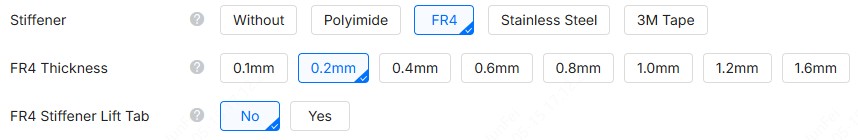
2.4.1 Select FR4 in the Stiffener field, then select the FR4 thickness. Multiple thicknesses may be selected according to the actual stiffener requirements in the Gerber files.
2.4.2 Select the FR4 Stiffener Pull Tab option if any part of the FR4 stiffener extends beyond the board outline or does not adhere to the board, because additional processing and procedures are required.
3. Stainless Steel Stiffener
3.1 Characteristics
- Extremely high mechanical strength: Stainless steel provides excellent local support for an FPC.
- Environmental resistance: Stainless steel resists high temperatures and also provides some heat dissipation.
- Strong rigid support: Due to its hardness, stainless steel stiffeners are mainly used in areas with extremely high rigid-support requirements.
3.2 Applications
For component protection: A steel stiffener can be added to the back of the core board beneath SMD components to prevent solder joints from detaching or pads and traces from breaking during bending. This stiffener also provides some heat dissipation. Steel stiffeners must not be used in Hall sensor areas.
3.3 JLCPCB Steel Stiffener Layer Naming Rules
| Type | Side | Specification | Naming Rule |
|---|---|---|---|
| Steel Stiffener | Top | 0.1, 0.2, 0.3 mm | gpt_* |
| Steel Stiffener | Bottom | 0.1, 0.2, 0.3 mm | gpb_* |
Example: a 0.2 mm steel stiffener on the top side can be named gpt_0.2.
3.4 Ordering Options and Notes
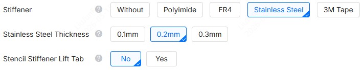
3.4.1 Select Stainless Steel in the Stiffener field, then select the stainless steel thickness. Multiple thicknesses may be selected according to the actual stiffener requirements in the Gerber files.
3.4.2 Select the Stainless Steel Stiffener Pull Tab option if any part of the stainless steel stiffener extends beyond the board outline or does not adhere to the board, because additional processing and procedures are required.
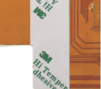
4. 3M Tape
4.1 Characteristics
- Strong adhesion, high-temperature resistance, and aging resistance provide a stable bond between the FPC and the attached component.
- Suitable for complex electronic-device operating environments, including temperature differences and humidity changes.
- Some models are compatible with processes such as SMT reflow soldering.
4.2 Applications
For convenient assembly and fastening: 3M Tape can be used where an FPC must be bonded and secured to an enclosure, bracket, or other external component. It offers strong adhesion, high-temperature resistance, and aging resistance, providing a stable bond while accommodating complex environments with temperature and humidity changes.
4.3 JLCPCB 3M Tape Layer Naming Rules
| Type | Side | Specification | Naming Rule |
|---|---|---|---|
| 3M Tape | Top | 3M468, 3M9077, tesa8854 | pst_* |
| 3M Tape | Bottom | 3M468, 3M9077, tesa8854 | psb_* |
Example: A tesa8854 Tape layer on the top side can be named pst_tesa8854.
4.4 Ordering Options and Notes
4.4.1 Select 3M Tape in the Stiffener field, then select the desired 3M Tape model.
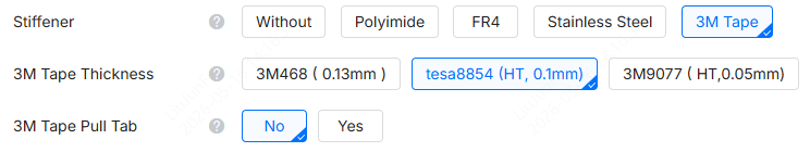
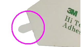
4.4.2 3M Tape Pull Tab Option
For easier removal of the release liner during assembly, select 3M tape with a pull tab. A small section of the 3M tape release liner extends beyond the board edge for easy removal during assembly. This option requires a special manufacturing process and incurs an additional charge.
4.4.3 Comparison of the Three 3M Tapes Currently Used by JLCPCB
| Parameter | 3M468 | 3M9077 | tesa8854 |
|---|---|---|---|
| Product Description | Unsupported acrylic transfer tape | Double-sided high-temperature tape with nonwoven backing | 3M Tape with nonwoven backing |
| Thickness | 0.13mm | 0.05mm | 0.1mm |
| Maximum Temperature Resistance | 200℃ | 260℃ | 260℃ |
| Long-term Temperature Resistance | 150°C (below 80°C recommended) | 150℃ | Below 80°C |
| Reflow Soldering Compatibility | Maximum temperature resistance is below the reflow soldering temperature | Designed for lead-free reflow soldering | Withstands reflow soldering at 260°C |
| Adhesion Performance | Extremely strong adhesion to metals: after 72 h at room temperature, peel strength is 129 N/100 mm on stainless steel, 126 N/100 mm on aluminum, and 101 N/100 mm on glass | 180° peel strength: 110 N/100 mm; after reflow: 91 N/100 mm | Initial adhesion to steel: 81 N/100 mm; after 14 days at room temperature: 94 N/100 mm |
| Die-cutting Performance | Suitable for curved surfaces and large-format die cutting | Suitable for precise, small-format die cutting | Suitable for general-purpose, standard-size die cutting |
| Key Advantages | Strong adhesion and chemical resistance | Thin and compatible with standard SMT processing | Better adhesion than 3M9077, compatible with standard SMT processing, and cost-effective |
| Key Disadvantages | Relatively thick; auxiliary material must be applied after SMT is completed | Unstable supply, significant price fluctuations, and average adhesion | Slightly lower long-term temperature resistance |
Electromagnetic Interference Shielding Film (EMI Shielding Film)
1 Characteristics and Introduction
EMI shielding film is a functional film applied to the FPC surface to shield electromagnetic interference and ensure signal stability. The EMI shielding film used by JLCPCB is 18 μm thick and black.
2 JLCPCB EMI Shielding Film Layer Naming Rules
| Type | Side | Specification | Naming Rule |
|---|---|---|---|
| EMI Shielding Film | Top | — | CSA |
| EMI Shielding Film | Bottom | — | SSA |
Example: An EMI shielding film layer on the top side can be named CSA.
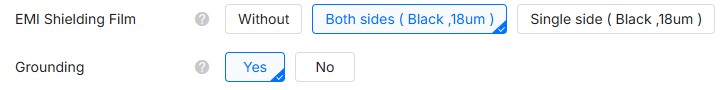
3 Ordering Options and Notes
Select the appropriate option according to the number of sides requiring EMI shielding film, and specify whether grounding is required. Note: EMI shielding film generally must be grounded.
4 Key Considerations When Using EMI Shielding Film
- EMI shielding film generally must be grounded. Without grounding, it absorbs a large amount of electromagnetic radiation and may cause abnormal signal transmission.
- To ground the EMI shielding film, add solder mask (coverlay) openings at least 1.0 mm in diameter over copper connected to the GND net. At least two openings are required. For a long flex cable, adding one approximately every 30 mm is recommended.
- EMI shielding film is conductive and must be kept at least 0.5–0.8 mm away from component pads.
- If EMI shielding film is applied locally, clearly mark the application area.
- EMI shielding film is not recommended in stiffener areas because it may cause the stiffener to detach. By default, JLCPCB removes the EMI shielding film beneath stiffeners and maintains a 0.5 mm clearance from stiffener areas.
Summary of JLCPCB Stiffener & EMI Layer Naming Rules
Using the same naming convention during the design stage is recommended. It reduces communication costs between design and production and makes engineering files easier to inspect and verify.
Although the naming rules for each type of stiffener layer are described above, they are summarized below for convenient reference:
| Type | Side | Specification | Naming Rule |
|---|---|---|---|
| PI Stiffener | Top | 0.1, 0.15, 0.2, 0.225, 0.25 mm | pit_* |
| PI Stiffener | Bottom | 0.1, 0.15, 0.2, 0.225, 0.25 mm | pib_* |
| Steel Stiffener | Top | 0.1, 0.2, 0.3 mm | gpt_* |
| Steel Stiffener | Bottom | 0.1, 0.2, 0.3 mm | gpb_* |
| FR4 Stiffener | Top | 0.1, 0.2, 0.4, 0.6, 0.8, 1.0, 1.2, 1.6 mm | fr4t_* |
| FR4 Stiffener | Bottom | 0.1, 0.2, 0.4, 0.6, 0.8, 1.0, 1.2, 1.6 mm | fr4b_* |
| 3M Tape | Top | 3M468, 3M9077, tesa8854 | pst_* |
| 3M Tape | Bottom | 3M468, 3M9077, tesa8854 | psb_* |
| EMI Shielding Film | Top | — | CSA |
| EMI Shielding Film | Bottom | — | SSA |
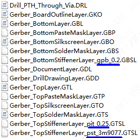
As illustrated below, in these exported Gerber files:
- gpb_0.2 indicates a 0.2 mm steel stiffener on the bottom side.
- pit_0.25 indicates a 0.25 mm PI stiffener on the top side.
- pst_3m9077 indicates 3M9077 3M Tape on the top side.
This concludes JLCPCB's brief introduction to FPC stiffeners and EMI. For any questions, please email support@jlcpcb.com.
The following documentation links may also be helpful.
- For the gold finger stiffener thickness calculator, refer to the following link: https://jlcpcb.com/gold-fingers-pi-thickness-calculator
- If you use JLCPCB's EasyEDA to design an FPC, refer to the following documentation: https://prodocs.easyeda.com/en/pcb/place-fpc-stiffener/index.html
- For more information about JLCPCB FPC production files and layer naming, refer to the following documentation: https://jlcpcb.com/help/article/how-to-confirm-the-production-file