
45 Must-Know Flex PCB Design Tips You Can't Afford to Miss!
8 min
- Outline and Drilling
- Copper Surface and Solder Pad Design
- Gold Fingers and Soldering
- Connector Pads and IC Design
- Silkscreen and Text Design
- Panelization Design
- Reinforcement Design
- Board Thickness
Achieving perfection in product design requires a careful balance between meeting design requirements and manufacturing standards. However, when it comes to flex PCB (FPC) design, many engineers find themselves at a loss, unsure of where to begin.
In this insightful guide, we will delve into 45 essential design guidelines for FPC. By the end, you'll have the knowledge and confidence to navigate the complexities of flex PCB design.
Outline and Drilling
1. The minimum distance from through-holes to the board frame should be 0.5mm. If less than 0.5mm, change to U-shaped holes (slots open towards the board frame).
2. Ensure via holes are at least 0.2mm away from the solder mask window to prevent exposed copper around the hole edges.
3. Avoid designing vias in pads in FPC, as unlike rigid PCBs, FPC cannot do resin plugging for such holes, leading to solder wicking.
Copper Surface and Solder Pad Design
4. Large Copper Surface Oxidation: Large copper areas can trap air during coverlay application, leading to oxidation in high temperature and pressure, affecting appearance but not function. To avoid this, design hatched copper or add solder mask windows on large copper surfaces.
5. Avoid Independent Pads: Independent pads, especially those overlapping on both sides, can easily detach since the FPC core is only 25μm thick. It’s recommended to add copper reinforcement around the pad and connect pad corners to the copper area, and offset pads on opposite sides for better adhesion.
6. Pad Detachment: Connector pads are prone to detachment. Design soldermask defined pads to prevent this, as the soldermask coverage on the pad’s rim provides mechanical strength.
7. Avoid Large Exposed Copper Areas: This can lead to wrinkling.
8. Coverlay Requirements: For flexible boards, coverlay acts as the solder mask. It needs to be pre-windowed before application. Ensure a 0.2mm gap between pads and adjacent traces, and a 0.5mm spacing between pads. Otherwise, bridged apertures should be used, accepting exposed traces.
9. Prevent Tearing at Corners: Sparse routing can cause tearing at board corners. Add anti-tear copper strips at the edges or add hatched copper on the back.
10. Grid Pattern Routing: Use a 45-degree angle for the grid pattern to improve signal transmission. Line width and spacing should be 0.2/0.2mm.
Gold Fingers and Soldering
11. Gold Fingers: Shrink gold fingers by 0.2mm to avoid micro-shorts caused by carbonization from laser cutting. (JLCPCB will do this by default; special requirements should be mentioned.)
12. Vias on Solder Pads: Avoid placing vias in a straight line on solder pads to prevent stress concentration and potential cracking.
13. Coverlay Offset: Ensure a 0.3mm offset for the coverlay on either side of gold fingers to prevent breakage.
14. Soldermask Defined Pads: Design solder pads with extended coverlay to ensure the coverlay overlaps the pad by more than 0.3mm.
15. Gold Finger Solder Mask Windows: Ensure windows overlap pads by more than 0.3mm to prevent disconnection at the joint.
16. Hollow Boards: JLCPCB currently does not support hollow boards. Reverse-side gold fingers need additional pads and vias for layer transitions.
17. Extra Copper on Pads: Avoid extra copper on IC pads, as this can enlarge pads and reduce spacing, leading to shorts during soldering.
18. Independent Gold Finger Pads: Design gold finger pads as independent pads. If there’s copper or traces overlapping the gold fingers, solder mask windows will expose the copper or traces.
19. Gold Finger Tolerance: Default tolerance is +/-0.1mm. If +/-0.05mm is required, specify when ordering.
Connector Pads and IC Design
20. Connector Pads: Connector pads in FPCs are prone to detachment. Design with soldermask defined pads to provide mechanical strength.
21. IC Bridges: Include coverlay bridges in the middle of ICs to retain the solder mask.
22. Gold Finger Solder Mask Windows: Gold finger pads must have solder mask windows to enable connection with the connector.
23. Default Solder Mask: Ensure the correct solder mask layer is used as the default.
24. Via Covering: To prevent cracking of via copper during bending, vias in FPCs are usually tented by default. Specify when ordering if coverlay windows are required.
25. Test Points: Do not attribute test points as vias, or separately add a window for test points.
26. Exposed Copper Edges: Large exposed copper areas on double-sided boards can blacken board edges. Add a coverlay ring around the edges.
Silkscreen and Text Design
27. If you need legend or silkscreen on the reinforcement, make sure to specify this when ordering to prevent process errors.
28. Avoid placing annotation text inside the board area or on the same layers as the rest of the design, as this could lead to unfortunate outcomes.
Panelization Design
29. For steel-reinforced boards, maintain a minimum distance of 3 mm between boards and a slot width of 0.5 mm, with connection points of 1 mm width spaced approximately every 15 mm. When ordering, specify paper to be placed between each PCB and sandwich between cardboard.
30. Avoid placing connection points on the same board edge as gold fingers, as this can cause unevenness at the front of the gold fingers.
31. Ensure there are enough connection points; each PCB should have at least two connection points of 0.8 mm width. The number of connection points should increase with the board size.
32. If the board is very small and has too many connection points, it can be hard to separate. If not for SMT, small PCBs need only two 0.3 mm connection points for easy manual separation.
33. Low utilization in panelization can lead to high costs (example below). Aim for a panel width of 119 mm or 240/250 mm, and consider choosing third-party panelization.
34. For very small boards less than 20 × 20 mm, panelize them to prevent the boards from being sucked away during laser dust collection. You can either deliver them as a panel or have JLCPCB help with the separation.
Reinforcement Design
Reinforcement involves adding rigid materials to specific areas of the FPC for easier assembly. PI reinforcement is suitable for products with gold finger insertion; FR4 is used for lower-end products; steel reinforcement is ideal for products requiring chip mounting due to its flatness and resistance to deformation.
35. Avoid using steel reinforcement over exposed pads as it may cause shorts. Additionally, steel has weak magnetism, making it unsuitable near Hall sensors. Steel reinforcement is also not recommended for gold finger areas.
36. Specify the total thickness requirement for gold finger insertion when ordering. The total thickness is usually in the connector specification sheet. Use JLCPCB's gold finger PI thickness calculator to determine the correct PI reinforcement thickness.
37. Reinforcement Cutouts: Design the reinforcement to avoid covering components or pads. Ideally, the customer should design this. If no cutouts are designed by the customer, JLCPCB defaults to cutouts for pads with a clearance of 0.3 mm. Any remaining reinforcement with width less than 2 mm will be removed, unless special requirements are specified in the order notes.
38. The reinforcement for gold fingers should extend at least 1.0 mm beyond the pad to prevent breakage during use.
39. Double-sided EMI films are electrically connected on both sides and cannot be separated. Consider removing EMI films if this is not acceptable for your design.
40. If a specific impedance to ground is required for the EMI film, design a soldermask opening over the ground trace/plane as the connection point to the film. Without specific requirements, JLCPCB defaults to adding a 1.0 mm solder mask window in a random location. Note: An ungrounded electromagnetic film may absorb significant electromagnetic waves, potentially causing signal issues, so verify with a prototype first.
41. Steel reinforcement on pads can cause shorts.
42. Reinforcement Width: FR4 reinforcement width less than 5 mm is prone to breaking and carbonization. Switch to PI or steel reinforcement. The minimum width for adhesive should be at least 3 mm.
43. Do not place reinforcement or adhesive near SMT pads, as it can interfere with stencil printing. If necessary, reinforcement or adhesive can be added after SMT.
Board Thickness
44. The selected board thickness includes coverlay, copper thickness, and PI board material thickness. If the board has non-copper areas or no coverlay, the thickness will be reduced accordingly. Pay special attention to this in your design.
45. FPC impedance calculations using simulation software can be inaccurate. JLCPCB’s empirical experience for designing line widths is available for reference, but always validate with a prototype first. This parameter applies to double-sided boards with 0.11 mm thickness.
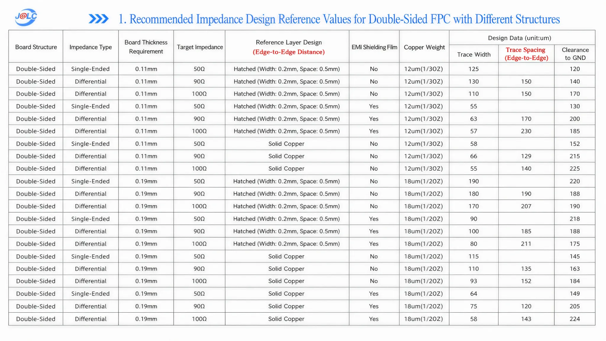
1. Recommended line width/spacing for hatched copper: 200 μm.
2. Grounding points (coverlay opening over ground place) are recommended on both sides when using EMI films. Recommended size: 1 × 1 mm.
3. The ground planes on both sides should be electrically connected by vias.
Note: All parameters above are based on the 0.11 mm 2-layer FPC stack-up.
JLCPCB’s design guidelines cover potential manufacturing issues, helping engineers identify manufacturability problems before production. This ensures various scenarios are met, minimizing design iterations and reducing costs!
Popular Articles
• 45 Must-Know Flex PCB Design Tips You Can't Afford to Miss!
• Choosing the Right Bend Radius for Durable Flexible PCBs
• FPC Design Rules: 13 Safety Distances You Can’t Ignore
• Mastering PCB Stiffeners: A Comprehensive Guide to Types, Applications, and Design Best Practices for Flexible Circuits
• How Flex Coverlay Protects and Enhances Flexible PCB Durability
Keep Learning
Flex PCB Manufacturing Process: From Prototyping To Mass Production
Flexible Printed Circuit Board commonly known as flex PCBs are a revolutionary step in modern electronics that offer compact, lightweight, dynamic and precise designs. Flex PCBs are designed to bend, twist, and fold, which rigid boards are incapable of. These characteristics have led to their widespread adoption in industries like wearable technology to consumer electronics to aerospace and medical technologies. With demands increasing day by day for miniaturized and ergonomic product designs, underst......
45 Must-Know Flex PCB Design Tips You Can't Afford to Miss!
Achieving perfection in product design requires a careful balance between meeting design requirements and manufacturing standards. However, when it comes to flex PCB (FPC) design, many engineers find themselves at a loss, unsure of where to begin. In this insightful guide, we will delve into 45 essential design guidelines for FPC. By the end, you'll have the knowledge and confidence to navigate the complexities of flex PCB design. Outline and Drilling 1. The minimum distance from through-holes to the ......
Choosing the Right Bend Radius for Durable Flexible PCBs
Key Takeaways Mastering the bend radius is essential for reliable flexible PCB design. Following IPC-2223 guidelines, maintain a minimum of 6× total thickness for static bends and 100× for dynamic applications, while using thinner RA copper, adhesiveless polyimide, staggered traces, and cross-hatched patterns in flex zones. Proper material selection, layer stackup optimization, and adequate clearance from stiffeners can dramatically extend flex life and prevent premature trace cracking or delamination......
FPC Connector Guide: Types, Pitch & Reliability
Key Takeaways Choosing the right FPC connector is critical for reliable flexible electronic designs. Connector type, pitch, pin count, stiffener thickness, and PCB layout all affect signal integrity and mechanical durability. By understanding FPC connector selection and design considerations, engineers can reduce connection failures and achieve reliable assembly results with JLCPCB. As you know, the electronics world is getting smaller; nowadays, the devices need to be thin and light. All the parts sh......
Flex PCB Design Guide: Preventing Mechanical Failures
Key Takeaways Reliable flex PCB design requires more than electrical performance. Proper bend radius control, trace routing, via placement, stiffener selection, and DFM considerations are essential to prevent mechanical failures such as copper cracking and delamination. By following proven flexible PCB design practices, engineers can improve durability and achieve reliable production results with JLCPCB. Ever wonder how the circuit in a foldable phone, fitness tracker, or camera module manages to rema......
Flex PCB Prototyping Guide: Materials & Design Tips
Key Takeaways A reliable flex PCB prototype requires more than just a working circuit. Material selection, bend radius control, copper design, panelization, and stiffener choices directly impact flexibility, durability, and manufacturing success. By following proper flexible PCB prototyping practices, engineers can reduce design risks and smoothly transition from prototypes to production with JLCPCB. Ever wonder how the circuit in a smartwatch, a foldable phone, or a camera module can take the shape? ......