PCIe Routing Guidelines: Layout Rules for High-Speed Design
19 min
- Key Takeaways
- Introduction
- PCIe Routing Requirements at a Glance
- Impedance and Trace Geometry
- Length Matching and Skew Requirements
- Reference Planes and Return Paths
- Vias, Corners, and AC Coupling Capacitors
- From Gen 3 to Gen 6: Loss Budgets and Materials
- PCIe Routing Checklist
- FAQs About PCIe Routing
- Conclusion About PCIe Routing

Key Takeaways
- CEM 5.0 specifies 72.5–97.5 Ω differential traces for its 16/32 GT/s slot channels; 85 Ω is the midpoint.
- The CEM specification requires intra-pair skew (mismatch within a pair) below 2.5 mils on the add-in card and 5 mils on the system board.
- Gen 5 operates at 32 GT/s with a 31.25 ps unit interval; Gen 6 retains that symbol interval through PAM4 signaling.
- PCI-SIG’s CEM-oriented example allocates 36 dB at 16 GHz to the complete Gen 5 channel, but only 16 dB to its baseboard.
Introduction
PCIe routing guidelines are a focused branch of high-speed PCB layout: set the differential impedance, match the two conductors of each pair, and keep the reference path continuous while the complete channel stays inside its loss and timing limits. A board that trains at reduced link width, or never establishes a link, can have a routing problem rather than a firmware problem. Those limits depend on the generation and topology; they do not all tighten by the same amount at each speed increase.
Define the channel before choosing a trace width. A short device-to-device link and a motherboard slot with an add-in card follow different electrical assumptions; the applicable PCI-SIG specifications and the selected silicon’s design guide set the layout constraints.
The sections below turn those constraints into routing decisions: a generation summary, stackup geometry, pair matching versus lane deskew, continuous return paths, component and via transitions, and a loss-budget method for choosing board materials.
PCIe Routing Requirements at a Glance
Set the rules for the right channel first. The PCI-SIG Base specification defines the electrical channel; the Card Electromechanical (CEM) specification defines the standard-slot implementation. Each lane carries full-duplex traffic on one transmit and one receive differential pair, and embedded timing still leaves a separate 100 MHz reference clock.
| Generation | Rate | Signaling | Symbol UI | Differential Trace Guidance | Complete-Channel Loss Reference |
|---|---|---|---|---|---|
| Gen 1 | 2.5 GT/s | NRZ | 400 ps | 100 Ω ±5%, TI guidance | Topology-specific; use its channel model |
| Gen 2 | 5 GT/s | NRZ | 200 ps | 68–105 Ω, CEM 3.0/5.0 | Topology-specific; use its channel model |
| Gen 3 | 8 GT/s | NRZ | 125 ps | 70–100 Ω, CEM 3.0/5.0 | 22 dB at 4 GHz |
| Gen 4 | 16 GT/s | NRZ | 62.5 ps | 72.5–97.5 Ω, CEM 4.0/5.0 | 28 dB at 8 GHz |
| Gen 5 | 32 GT/s | NRZ | 31.25 ps | 72.5–97.5 Ω, CEM 5.0 | 36 dB at 16 GHz |
| Gen 6 | 64 GT/s | PAM4 | 31.25 ps | Consult CEM 6.0 and the device design guide | 32 dB at 16 GHz |
CEM ranges are absolute limits that already include manufacturing variation; TI’s ±5% is separate vendor guidance, and no CEM 6.0 impedance tolerance is quoted here. Loss figures are PCI-SIG’s total-channel planning values, including package and connector allocations, not bare-board allowances. Rates and symbol intervals: Base 6.0, Table 8-10.
Gen 6 sends two bits per PAM4 symbol at 32 GBd, so its symbol interval is 31.25 ps, not 15.625 ps. Its smaller vertical eye openings make channel quality more demanding despite retaining Gen 5’s 16 GHz Nyquist frequency.
PCIe Routing Rules Quick Reference
Use these values as the starting rules for a standard-slot (CEM) channel, then confirm them against the applicable specification revision and your silicon vendor's design guide.
| Rule | Target Value | Where It Applies | Source |
|---|---|---|---|
| Differential impedance | 85 Ω design target; CEM windows: 68–105 Ω at 5 GT/s, 70–100 Ω at 8 GT/s, 72.5–97.5 Ω at 16/32 GT/s | Add-in card and system board traces | PCI-SIG CEM 3.0 / 4.0 / 5.0 |
| Intra-pair skew | ≤2.5 mil (0.064 mm) on the add-in card; ≤5 mil (0.127 mm) on the system board | The two conductors of each differential pair | PCI-SIG CEM 4.0; TI SLAAE45 (5 mil) |
| Via stub | Below 15 mil; back-drill longer stubs | Through-vias on Gen 4/5 pairs | TI SLAAE45 |
| AC-coupling capacitors | 176–265 nF at 8 GT/s and above; 75–220 nF in TI's Gen 4 note | One in each conductor of the transmitter path | PCI-SIG Base 6.0, Table 8-7; TI SLAAE45 |
| Capacitor placement | Near the transmitter, both parts aligned; CEM 5.0 assigns them to transmitter pairs | TX side of each lane | PCI-SIG Base 6.0 / CEM 5.0 |
| Corners | Two 45° bends or a smooth arc; avoid 90° | Whole differential pair | TI SLAAE45 |
Slotless chip-to-chip links follow the silicon vendor's guide instead, and 100 Ω belongs to older Gen 1/2 vendor guidance rather than to these CEM slot windows.
Impedance and Trace Geometry
Set the PCIe impedance target before drawing the route. A width copied from another board has no meaning without its dielectric height, copper thickness and pair spacing. Agree the stackup with fabrication, solve the pair geometry, then enter that geometry as routing rules rather than correcting it after fanout.
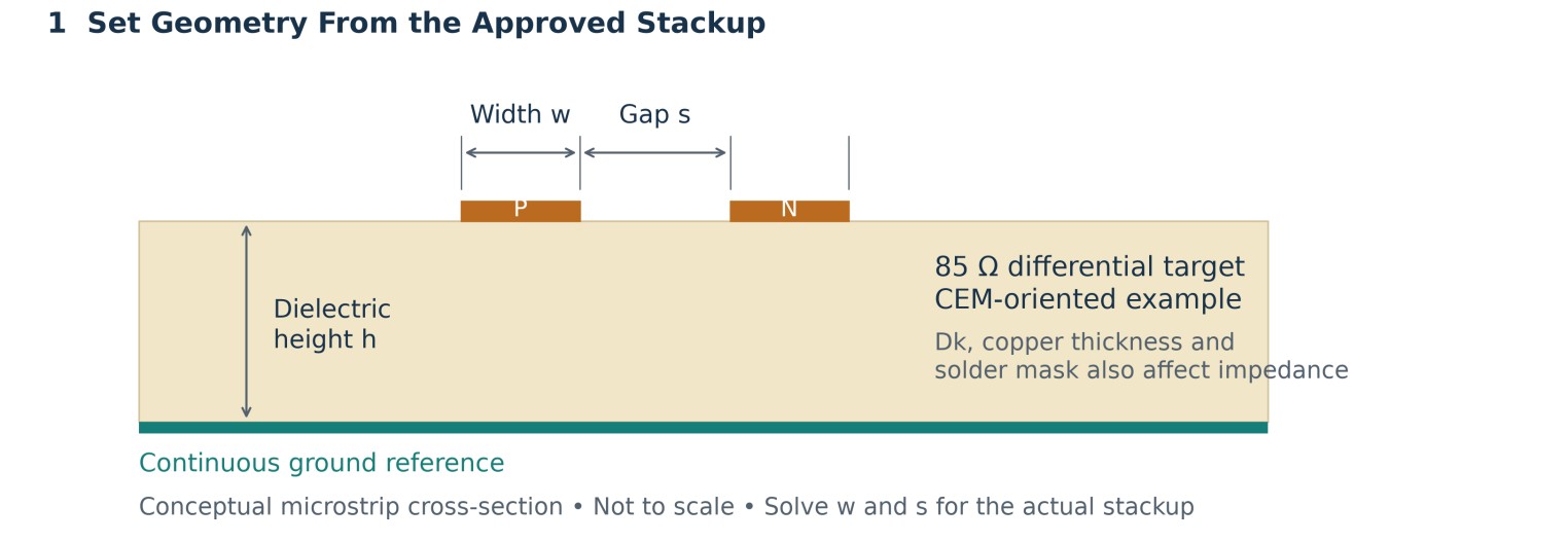
Figure 1. Width, gap and dielectric height jointly set differential impedance. Conceptual cross-section, not to scale; use the approved stackup rather than deriving dimensions from this drawing.
Differential Impedance Targets by Generation
85 Ω or 100 Ω? For standard-slot channels, check the actual CEM window: CEM 3.0 specifies 68–105 Ω at 5 GT/s and 70–100 Ω at 8 GT/s. The 72.5–97.5 Ω window used from 16 GT/s onward first appears in CEM 4.0, and CEM 5.0 carries it for its 16/32 GT/s channels. Do not replace these absolute limits with an approximate percentage, or extrapolate the window to Gen 6 without the applicable CEM revision.
These trace requirements exclude vias, connectors, package traces and cables. Slotless links follow their silicon guide instead: Qualcomm’s QRB5165 guide permits 70–100 Ω differential field routing, including manufacturing variation.
TI pairs 100 Ω differential with 50 Ω single-ended for Gen 1/2, and 85 Ω with 42.5 Ω for Gen 3/4. Take these as that document’s matched values: because the two conductors couple, a single conductor’s impedance is not simply half the pair’s differential impedance.
Hitting 85 Ω on a Real Stackup
For a slot channel targeting 85 Ω, ask fabrication for finished dielectric thickness and the material’s design Dk. Wider traces generally lower impedance; a larger separation from the plane raises it, while bringing the pair members closer increases coupling and lowers differential impedance. Change these variables together, not independently.
Loosely coupled pairs rely more heavily on their planes. Tightly coupled pairs are more sensitive to local changes in pair gap. Either approach needs symmetry through breakouts, bends and component pads.
Moving from a 4-layer to a 6-layer board may provide a better-referenced routing corridor, but extra layers do not establish impedance by themselves. Enter the fabricator-approved stackup and trace geometry as design rules in EasyEDA, then verify the target with the impedance calculator in your EDA tool or JLCPCB’s online impedance calculator before release.
Length Matching and Skew Requirements
Match the two conductors within each differential pair; lanes do not need equal physical lengths. Keep those two constraints separate in the rule set. Pair imbalance distorts the differential waveform, while lane-to-lane arrival differences are absorbed by receiver timing recovery and link deskew — within finite limits.
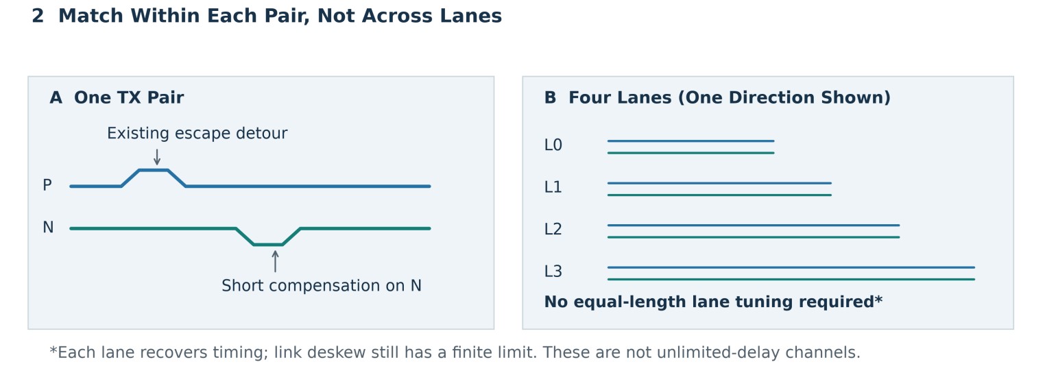
Figure 2. Local compensation balances the conductors within a pair; separate lanes need not share a common length. Conceptual routes, not to scale. Link deskew limits still apply.
Intra-Pair Skew: Keep Each Pair Tight
The CEM specification requires intra-pair skew (mismatch within a pair) below 2.5 mils on the add-in card and 5 mils on the system board (0.064 mm and 0.127 mm), limits first defined in the CEM 4.0 revision. TI’s general Gen 4 application note recommends 5 mils, which must not override a stricter applicable card requirement.
An imbalance makes the two transitions arrive at different times, causing differential-to-common-mode conversion and reducing the useful eye opening. Gen 3’s 125 ps symbol interval falls to 31.25 ps at Gen 5; the same board delay mismatch occupies a larger fraction of the latter interval.
Correct an escape imbalance locally, then keep the route balanced. Use modest tuning increments on straight sections away from capacitor pads and signal vias. Avoid tightly packed serpentines that replace a small mismatch with a larger impedance disturbance. Check electrical delay where the tool and device model support it; equal centerline lengths alone do not account for different layers, package paths or glass-weave exposure.
Lane-to-Lane Skew: Why PCIe Does Not Need Equal-Length Lanes
PCIe lane to lane skew does not require ordinary lanes to have equal trace lengths. Each receiving lane recovers timing from its data; elastic buffering and lane-deskew logic allow the receiver to realign traffic across a multilane link.
That is not permission for unlimited delay differences. The CEM specification allocates 1.6 ns to total interconnect skew: 0.35 ns on the add-in card and 1.25 ns on the system board, excluding transmitter output skew. That budget dates from CEM 3.0. Apply the actual form-factor and component limits rather than an arbitrary equal-length rule.
On an x16 connection, stretching short lanes to match the longest route adds copper, loss and coupling opportunities without improving intra-pair balance. Route each lane directly, preserve its own pair geometry, and check the worst channel independently. A compact route with clean transitions is usually a better starting point than a bank of meanders added only to make the length report look uniform.
The 100 MHz Reference Clock
Route REFCLK as a 100 MHz differential clock, separate from the serial-data lanes: match its pair internally, reference it to continuous ground, and keep it clear of switching-regulator fields and plane splits.
In a common-clock architecture, both link partners derive their reference from the same source. SRNS uses separate references without spread-spectrum modulation; SRIS uses separate references with independent spread-spectrum modulation and requires compatible devices.
The clock pair does not need to equal the data-pair lengths. Common-clock timing still depends on clock-distribution delay and the data path, so check the platform’s architecture-specific delay and jitter requirements rather than inventing a universal maximum trace length. Give the clock a quiet routing corridor alongside the channel, with separation from its data aggressors and noisy supplies.
Reference Planes and Return Paths
Inspect the reference copper under the entire pair on every layer the route crosses. A route can pass clearance checks while crossing a slot, a chain of overlapping antipads or a narrow copper neck. Each creates a reference discontinuity that the pair’s neat appearance conceals.
Differential signaling does not make the reference plane irrelevant. Fields still interact with the plane, and imbalance creates common-mode current that needs a local return path. Route both conductors over continuous reference copper. If a plane split blocks the corridor, move the route or fix the stackup; adding length to preserve continuity is preferable to accepting an uncontrolled crossing.
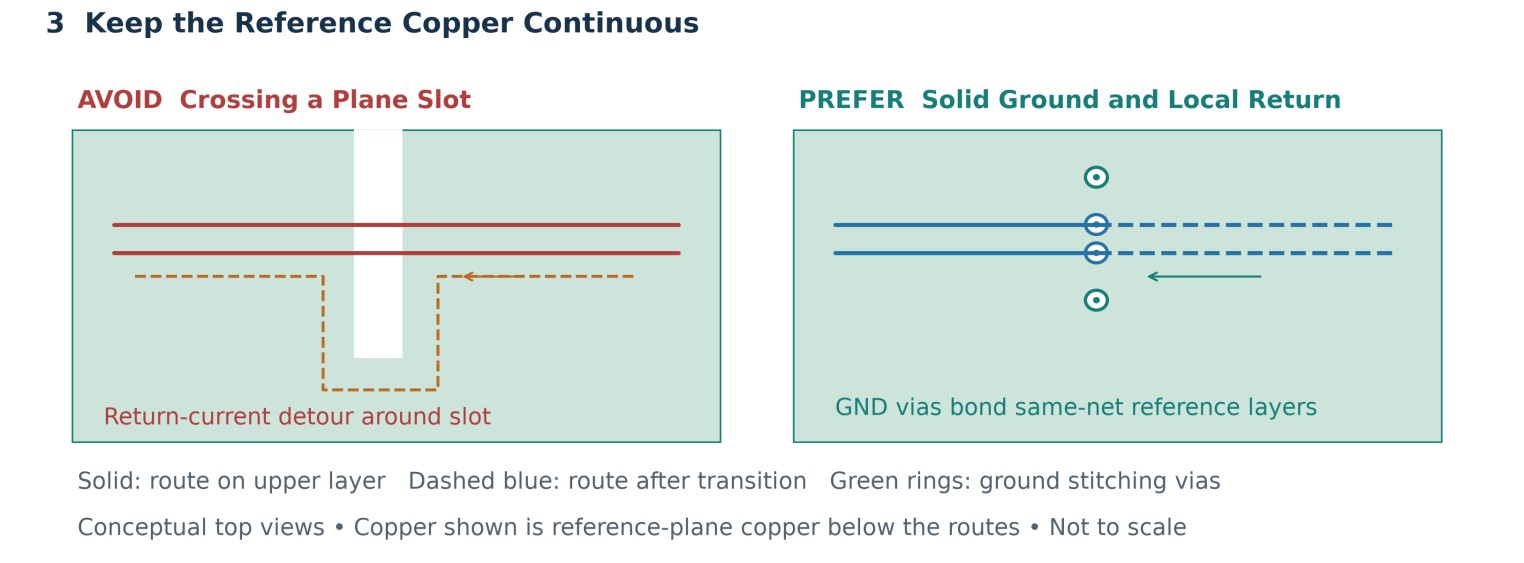
Figure 3. A slot forces reference current around a detour. At a layer transition, nearby ground vias connect same-net ground references. Conceptual top views, not to scale; dashed blue traces represent the destination layer.
Keep a pair on one layer where practical. When it changes layers between ground-referenced corridors, place ground stitching vias beside the signal transition so reference current can change planes nearby. Both planes must actually be ground: a stitching via must never short a power plane to ground.
Look carefully at BGA escape fields and edge-connector launches. Signal-via antipads can merge into a barrier, while excessively broad connector keep-outs can remove reference copper from the approaching route. Use local voids only where the approved footprint or a transition model calls for them. A controlled pad-capacitance correction is different from routing across an arbitrary plane gap.
In PCIe PCB layout, this review belongs after copper pours and clearances are finalized, not only during initial routing. JLCPCB’s ground-plane and power-plane guide provides the broader stackup context; use the device and connector reference layouts for the actual launch geometry.
Vias, Corners, and AC Coupling Capacitors
A uniform trace is only part of the channel. Pads, bends and vertical transitions change the field geometry and can introduce reflections or mode conversion. Review those features as connected structures, rather than assuming that an impedance rule applied to straight tracks also qualifies the transitions.
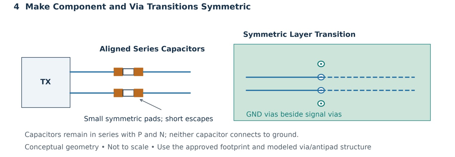
Figure 4. Align the series capacitors and keep signal-via transitions symmetric, with adjacent same-net ground stitching. Conceptual geometry, not to scale; use approved footprints and modeled pad/antipad dimensions.
Via Count and Stub Control
Minimize layer transitions before adding back-drilling to rescue them. Both conductors should see the same number of vias and comparable pad, antipad and barrel geometry. A symmetric transition reduces imbalance, but symmetry does not remove its insertion loss.
A through-via can leave an unused barrel below the destination layer. That stub behaves as a resonant structure; a longer stub puts its resonance lower in frequency. TI’s Gen 4 application note recommends stubs below 15 mils and back-drilling longer ones, within that application’s guidance.
For Gen 4/5 channels, review stub length with the fabricator’s achievable back-drill residual and the channel model. Blind or buried structures may be alternatives where the stackup supports them. Count transitions in the exported layout and model the actual structure, including nearby ground vias, rather than treating every via as an identical fixed penalty.
Bends: 45° Corners and Curves
Avoid abrupt 90° corners on multi-GT/s pairs. Use two 45° bends or a smooth arc and preserve spacing through the turn, as TI recommends. The reason is impedance consistency, not a claim that one right-angle corner automatically turns the trace into a radiating antenna.
Inspect both conductors after tuning: a smooth outer trace can hide a pinched inner gap. Do not add a large detour solely to improve an already modest bend. Compare the complete geometry, then favor the shorter route that preserves the intended pair spacing.
AC Coupling Capacitor Placement
Put a series coupling capacitor in each conductor of the transmitter path, following the topology’s placement rules. Each link partner supplies coupling for its own transmitted data; adding another set automatically at every receiver can create unintended double coupling.
The required range depends on the specification revision. Base 6.0, Table 8-7, specifies 176–265 nF; TI’s Gen 4 layout note lists 75–220 nF. Qualcomm lists 75–265 nF for its Gen 2 implementation and 176–265 nF for its Gen 3 case. Check the applicable specification, component tolerance and device guide rather than copying a legacy value.
Place the capacitors near the transmitter where the approved topology permits. Base 6.0 requires the form-factor specification to define their location at a pluggable interface; CEM 5.0 assigns them to transmitter pairs. Align the components instead of staggering them. Keep escapes short and symmetric, with compact pads and local reference-plane relief only where supported by the footprint model.
From Gen 3 to Gen 6: Loss Budgets and Materials
Treat the dB values below as channel allocations, not trace-length allowances: they include package and connector losses. The numbers come from PCI-SIG’s CEM-oriented planning example, and the baseboard column is the motherboard’s share only.
| Generation | Nyquist Frequency | Total Channel | Baseboard Share, Example | Material Candidates, Subject to Channel Analysis |
|---|---|---|---|---|
| Gen 3 | 4 GHz | 22 dB | 10.3 dB | Standard-loss 370HR; lower loss for longer routes |
| Gen 4 | 8 GHz | 28 dB | 13.5 dB | Mid-loss FR408HR; lower-loss I-Speed or MEGTRON6 |
| Gen 5 | 16 GHz | 36 dB | 16 dB | Low-loss I-Speed; lower-loss MEGTRON6, I-Tera MT40 or Tachyon 100G |
| Gen 6 | 16 GHz | 32 dB | 14 dB | Low/very-low-loss candidates, qualified for PAM4 margin |
Isola supplies the 370HR, FR408HR and I-Speed examples. Panasonic’s MEGTRON6 and Isola’s I-Tera/Tachyon data supply the remaining candidates. These are manufacturer examples, not PCI-SIG material approvals.
For Gen 5, the example subtracts 9 dB for the root-complex package, 1.5 dB for the connector and 9.5 dB for the add-in-card allocation: 36 − 9 − 1.5 − 9.5 = 16 dB left for the baseboard, all at 16 GHz. Do not subtract the add-in-card package again if it is already inside that allocation.
Screen materials in three practical tiers: standard-loss 370HR, intermediate FR408HR, and lower-loss candidates starting with I-Speed; MEGTRON6, I-Tera MT40 and Tachyon 100G extend the list. These tiers are relative, not a standardized rating. Compare each product’s construction, test frequency, foil roughness and supplier loss model.
Standard-loss FR-4 can suit many Gen 3 channels; it is not guaranteed even there. Short Gen 4 routes may close on intermediate-loss material, while long Gen 5/6 channels often benefit from lower-loss laminates. Generation alone does not prescribe the material.
For roughly constant loss tangent, dielectric attenuation grows approximately with frequency; smooth-conductor skin-effect attenuation grows approximately with its square root. Roughness and dispersion complicate that comparison. Use full-channel S-parameters and the device’s receiver/equalization model before declaring the material adequate.
PCIe Routing Checklist
| Check Item | What to Verify | Tip/Tool |
|---|---|---|
| Channel Definition | Correct generation, slot topology and applicable device guides | Freeze the channel endpoints before setting rules |
| Impedance | Approved target and fabrication tolerance on every routing layer | EasyEDA impedance calculator where available, or JLCPCB’s calculator; confirm with impedance coupons |
| Plane Continuity | No split or antipad barrier under either conductor | Inspect final reference-layer copper and exported files |
| Pair Matching | Within-pair mismatch meets the selected device’s constraint | Use EasyEDA length checks and the length-matching guide |
| Lane Deskew | Delay spread stays inside platform limits without equal-length meanders | Review longest and shortest channels, including packages |
| Coupling Capacitors | Correct value, tolerance, location and coupling count | Cross-check schematic, BOM and device reference layout |
| Vias | Symmetric transitions, local ground return and controlled residual stubs | Review back-drill drawing and transition models |
| Crosstalk | Adequate spacing from neighboring pairs and switching circuits | Apply device spacing rules; inspect dense escape corridors |
| Reference Clock | Architecture, internal pair balance and quiet reference path | Check clock-driver routing and jitter guidance |
| Add-in-Card DFM | Gold fingers, bevel, connector footprint and impedance coupons | Run EasyEDA DRC, then fabricator and CEM mechanical checks |
FAQs About PCIe Routing
What Differential Impedance Should PCIe Traces Be?
Older Gen 1/2 designs commonly used 100 Ω, but standard-slot channels from CEM 3.0 onward center on 85 Ω: 68–105 Ω at 5 GT/s, 70–100 Ω at 8 GT/s (CEM 3.0), and 72.5–97.5 Ω at 16/32 GT/s (CEM 5.0). The edge connector is itself 85 Ω, so the traces between it and the IC should be 85 Ω. A slotless chip-to-chip link follows the silicon vendor’s guide instead.
Do PCIe Lanes Need to Be Length-Matched to Each Other?
No, PCIe lane to lane skew does not demand equal-length lanes, but it must remain within the link’s finite deskew allowance. Match each pair internally and remove unnecessary lane-equalization meanders rather than spending loss budget on cosmetic length uniformity.
Where Do PCIe AC Coupling Capacitors Go?
They belong in the transmitter’s signal path, with placement controlled by the applicable topology and device guide. Use the CEM add-in-card rules where relevant; do not duplicate capacitors at the receiver merely because another interface places them there.
Is There a Maximum Trace Length for PCIe?
No single maximum applies, but the budget does. PCI-SIG’s Gen 6/7 signal-integrity guidance assumes at least 13 inches of baseboard routing plus 4 inches on the add-in card. Those lengths fit the Gen 6 allocation of 32 dB at its 16 GHz Nyquist frequency; Gen 7 doubles the Nyquist frequency to 32 GHz and uses a separate loss budget, so the 32 dB @ 16 GHz figure does not apply to it. Reach depends on material, discontinuities, crosstalk and receiver capability, so check the vendor’s limit and analyze the assembled channel rather than converting a dB budget into inches.
Conclusion About PCIe Routing
Useful PCIe routing guidelines start with the right impedance target, balance the conductors within each pair and preserve their reference path. They also distinguish pair matching from finite lane deskew: equal-length lanes are not the objective. A route must satisfy the electrical limits of its actual topology, including packages, connector launches and coupling components.
Choose the laminate from the remaining board loss allocation, not a blanket rule about generation. Inspect transitions and final plane copper before spending time on elaborate tuning. At higher speeds, a clean length report and an empty DRC list still do not establish channel compliance.
For connector signal assignments and gold-finger contact numbers, use the PCIe pinout reference alongside this layout checklist. When you are ready to hand off placement and routing, upload your schematic and channel requirements to JLCPCB’s professional PCB layout service.
Keep Learning
PCIe Routing Guidelines: Layout Rules for High-Speed Design
Key Takeaways CEM 5.0 specifies 72.5–97.5 Ω differential traces for its 16/32 GT/s slot channels; 85 Ω is the midpoint. The CEM specification requires intra-pair skew (mismatch within a pair) below 2.5 mils on the add-in card and 5 mils on the system board. Gen 5 operates at 32 GT/s with a 31.25 ps unit interval; Gen 6 retains that symbol interval through PAM4 signaling. PCI-SIG’s CEM-oriented example allocates 36 dB at 16 GHz to the complete Gen 5 channel, but only 16 dB to its baseboard. Introductio......
RF PCB Layout: Common Design Mistakes and Practical Guidelines
Key Takeaways Impedance control is non-negotiable: Maintain consistent 50Ω impedance across all transitions, including vias, connector launches, and trace bends, to prevent reflections and signal loss. Return path integrity determines RF success: Never route RF traces over ground plane splits or slots. Provide continuous return paths with stitch vias at every layer change. Functional zoning prevents interference: Physically separate RF front-end circuitry from digital logic and power management to kee......
High Speed PCB Layout Guide for Reliable Signal Control
Key Takeaways 1. High-speed ≠ high frequency alone — it's defined by signal edge rates and trace electrical length. Treat traces as transmission lines with controlled impedance, not simple wires. 2. Placement is an electrical decision — clustering drivers/receivers, matching differential pairs symmetrically, and keeping decoupling capacitors tight to power pins directly govern signal integrity. 3. Continuous ground planes are non-negotiable — never route high-speed traces across split planes; use stit......
High-Speed PCB Routing: Guidelines, Techniques & Examples
Key Takeaways 1. Define "High-Speed" by Rise Time, Not Clock Frequency. Per IPC-2251, traces longer than 2 x rise_time require controlled impedance routing. Even sub-100 MHz signals with fast edges demand transmission-line treatment. 2. Plan the Stackup Before Routing. Every high-speed signal needs an uninterrupted reference plane. Use the fabricator's actual impedance data—JLCPCB guarantees ±10% tolerance on controlled impedance. 3. Route Critical Nets in Priority Order. Route clocks, differential pa......
LVDS PCB Layout Guidelines: Design Tips and Worked Example
Key Takeaways 100 Ω Differential Impedance: LVDS PCB layout starts with one number: 100 Ω of differential impedance. Trace width, spacing, and board thickness all set that number. Route Pairs Together: Route the two traces of a pair together, side by side, and keep their lengths within 5 to 10 mil of each other. Solid Ground Plane: Never let an LVDS pair cross a gap in the ground plane. It breaks the return path and hurts the signal. 4-Layer Minimum: A 4-layer board with a solid ground plane is enough......
Crosstalk in PCB Design: Causes, Types, and How to Reduce It
Key Takeaways Crosstalk starts at an edge: a changing aggressor voltage and current produce electric and magnetic fields that couple energy into a neighboring victim trace. Edge rate matters more than clock frequency alone. A modest-rate bus with fast I/O edges can still create a serious coupling problem. More spacing and a smaller signal-to-reference-plane distance usually provide the cleanest layout improvements, but the result depends on the complete cross-section. NEXT and FEXT do not scale in the......