
RF PCB Layout: Common Design Mistakes and Practical Guidelines
12 min
- Why RF PCB Layouts Fail: Top 5 Common Design Mistakes
- RF PCB Design Guide to Component Placement: The Zoning Strategy
- RF Routing Guidelines: Mastering 50Ω Impedance Control
- SMA Connector PCB Layout: Professional Transition Design
- RF PCB Design Guidelines: The Physics Behind Every Layout Rule
- Advanced RF Layout Guidelines for High-Performance Boards
- From Design to Manufacturability: Why Fabrication Precision Matters in RF
- FAQ about RF PCB Layout
Key Takeaways
Impedance control is non-negotiable: Maintain consistent 50Ω impedance across all transitions, including vias, connector launches, and trace bends, to prevent reflections and signal loss.
Return path integrity determines RF success: Never route RF traces over ground plane splits or slots. Provide continuous return paths with stitch vias at every layer change.
Functional zoning prevents interference: Physically separate RF front-end circuitry from digital logic and power management to keep harmonics and switching noise out of the receive band.
Via design matters at high frequencies: Eliminate via stubs through back-drilling or microvias, and always pair signal vias with ground-stitching vias to maintain 50Ω through layer transitions.
Material selection limits performance: Above 2 GHz, FR-4’s dielectric losses degrade signal quality. Use RF-grade laminates like Rogers RO4350B or Megtron 6 for controlled impedance and low loss.
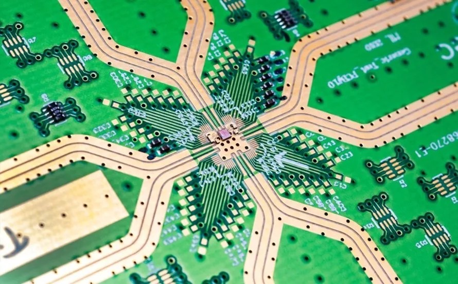
Designing a radio-frequency printed circuit board is a discipline in which physics sets the rules. In an RF PCB layout, all copper features are transmission lines that not only transmit signals but also shape them based on their physical geometry.
At gigahertz frequencies, signals obey the laws of wave propagation, not Kirchhoff’s laws, and the “best practices” developed over years of digital design can sneakily undermine an RF system’s performance.
New wireless technologies such as 5G NR, Wi-Fi 6E, and UWB are extremely unforgiving. Reflections, higher noise floor, and even non-compliance can result from a single impedance mismatch or misplacement of a via.
This RF PCB design guide cuts straight to the causes of those failures and what to do about them.
Why RF PCB Layouts Fail: Top 5 Common Design Mistakes
Most RF failures aren’t schematic problems. They’re physical implementation problems that only appear once a board is assembled.
1Impedance Discontinuities at Transitions
Consistent 50Ω impedance is the primary requirement for any RF system. Structural changes like sudden width shifts, pad transitions, or uncompensated vias disrupt this balance. These discontinuities create reflections that degrade VSWR and increase insertion loss, potentially suppressing the signal-to-noise ratio below the system’s link budget.
2Ignoring Return Path Integrity
High-frequency return current follows the path of least inductance, directly beneath the signal trace. Slots, voids, or splits in the ground plane force the current to detour. This enlarged loop introduces parasitic inductance, causes ground bounce, and turns the trace into an unintentional antenna.
3Improper Via Usage
Standard through-hole vias introduce parasitic inductance that can completely disrupt a 50Ω path at high frequencies. Furthermore, unused via stubs act as resonant structures. These stubs create sharp attenuation notches at specific frequencies, effectively killing the signal. High-performance designs must use back-drilling or microvias to eliminate these stubs.
4Poor Functional Partitioning (RF vs. Digital)
Digital logic generates harmonics that bleed into the GHz spectrum. Without strict spatial separation, a 100 MHz clock can easily interfere with an LTE receive window. RF front-ends must be physically sequestered from digital zones and switching regulators to maintain a clean noise floor.
5Right-Angle Traces and Sudden Bends
A 90° bend increases the effective trace width at its corner apex. This creates a localized increase in parasitic capacitance and a corresponding impedance dip. These dips cause reflections that accumulate across multiple corners. Sharp angles also concentrate electric fields, increasing radiation loss. Use 45° mitered bends or smooth circular arcs to maintain signal integrity.
RF PCB Design Guide to Component Placement: The Zoning Strategy
A clean RF layout starts with a disciplined floor plan, not the router.
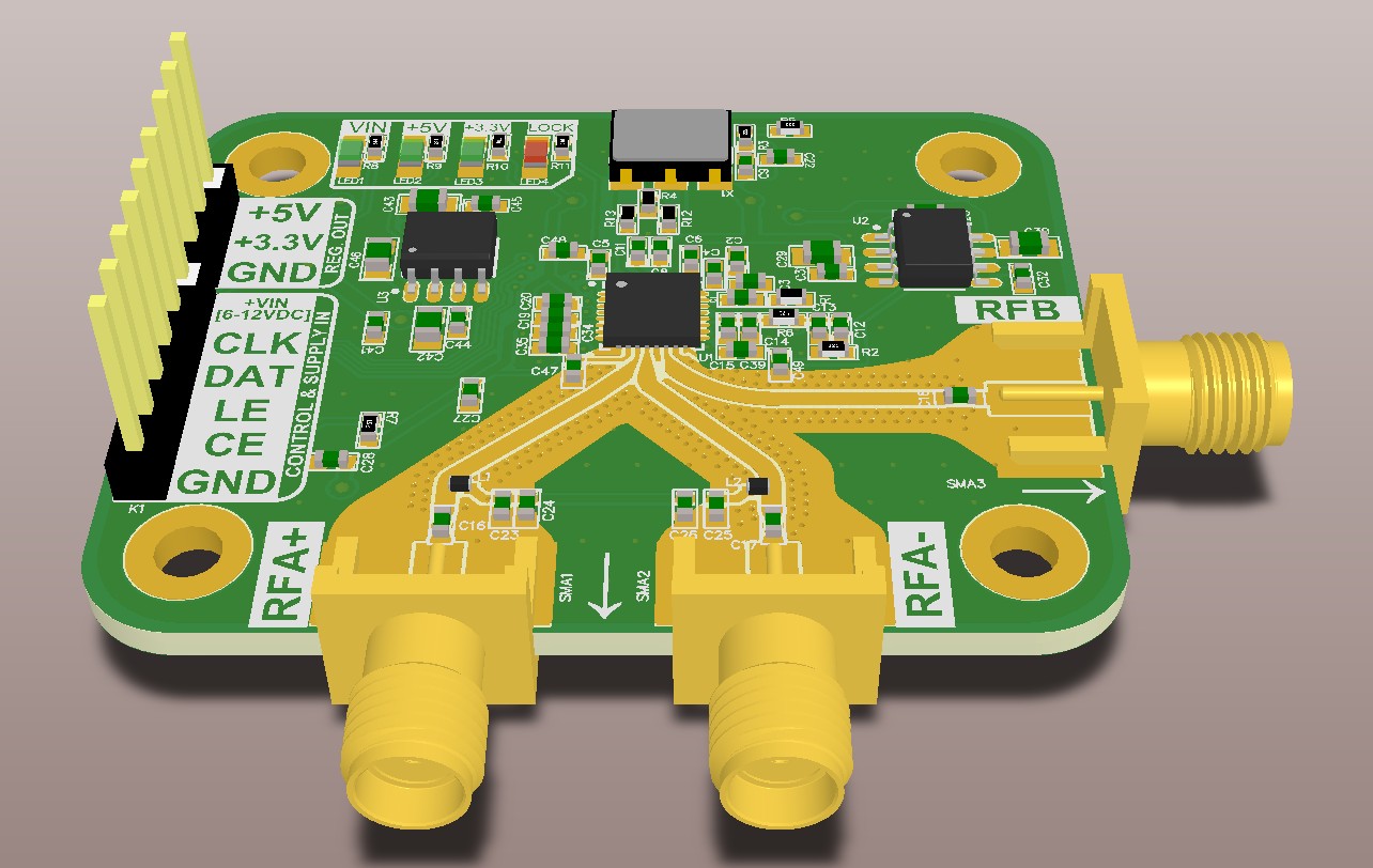
Functional Zoning: Strict RF / Digital / Power Separation
Divide the board into distinct geographic zones: RF front-end, digital processing, and power management, each treated as a separate electromagnetic domain. The RF zone (antenna interface, LNA, PA) must be physically sequestered from the digital zone.
Switching regulators belong in their own isolated region since their transients couple into both domains. A 20 mm separation is a practical starting point; high-density designs will need via fences or shielding cans to compensate.
Straight-Line Signal Chain Principle
The RF path from the antenna connector through filters, amplifiers, and matching networks to the transceiver should follow a straight, linear sequence.
Every unnecessary turn or layer transition introduces parasitic reactances that must later be compensated with bench tuning.
Placing Critical Components Close Together
In RF design, physical distance is an electrical parameter. Matching network components must sit immediately adjacent to IC pins. Any trace between them adds unintended series inductance, shifting the matching frequency.
The same applies to decoupling capacitors: keep the area between the capacitor and the IC power pin small. Using a mix (100 pF, 0.01 µF, 0.1 µF) of values in parallel provides a low-impedance connection to ground over a broad range of frequencies.
RF Routing Guidelines: Mastering 50Ω Impedance Control

If you truly want to handle the 50Ω Impedance Control, you must follow the RF routing guidelines like the following.
Calculating and Maintaining 50Ω Trace Width
Characteristic impedance depends entirely on the trace’s cross-sectional geometry and the substrate’s dielectric properties. For a microstrip on standard 1.6 mm FR-4 with 1 oz copper, 50Ω falls around 2.8 mm, but this shifts with every stackup parameter.
Use a manufacturer-provided impedance calculator to determine the exact width for your specific build. Once established, hold that width with precision. A 10% variation in width produces measurable reflections above 3 GHz.
Avoiding Right Angles: Use 45° Bends or Arcs
The 45° miter removes excess copper at the corner apex, compensating for the localized increase in capacitance. Above 10 GHz, smooth arcs are preferred over a discrete bend, even at 45°, which still represents an abrupt change in effective dielectric constant at millimeter-wave frequencies.
Minimizing Trace Length and Managing Via Parasitics
Keep RF traces as short as possible. Dielectric loss increases with both frequency and length, so every unnecessary millimeter erodes the link budget. When a layer change is unavoidable, engineer the via as a 50Ω structure by surrounding the signal via with at least two closely spaced ground-stitching vias. These provide a local return path, confine the electromagnetic fields, and prevent the via from radiating into the surrounding dielectric.
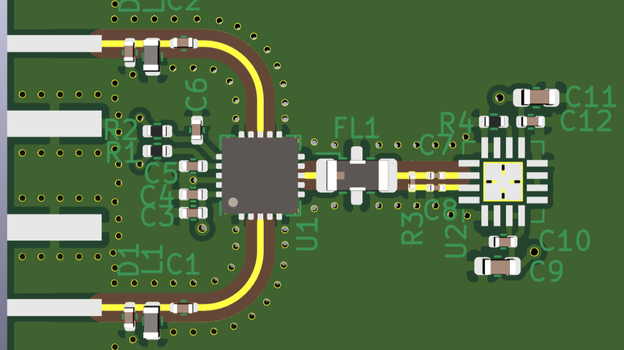
SMA Connector PCB Layout: Professional Transition Design
The SMA connector is the handshake between the coaxial environment and the PCB. Done poorly, it becomes the board’s primary reflection source. Here’s how the SMA connector PCB layout works–
50Ω Transition Structure at the SMA Footprint
The SMA center pin is wider than a standard 50Ω trace, creating a capacitive bump at the entry point. A tapered launch gradually widening the trace to meet the connector pad smooths this transition and keeps local impedance variations within bounds.
For high-frequency applications, an anti-pad (a void in the reference plane beneath the signal pad) reduces parasitic capacitance to ground. Its exact geometry should be validated with a full-wave EM simulation for the specific stackup.
Ground Pad and Via Stitching at the Connector
Each ground tab on the SMA connector requires multiple vias placed directly beneath it, forming a via wall that connects the connector’s reference to the board ground with minimal inductance.
This fence should encircle the signal launch, contain the electromagnetic fields, and suppress edge-mode resonances within the operating band.
RF Path Length Control and Connector Placement
Place SMA connectors at the board perimeter to minimize RF path length to active components. For edge-mount types, the trace must extend to the exact board edge. Any copper pull-back creates a parasitic stub that degrades return loss at higher frequencies.
RF PCB Design Guidelines: The Physics Behind Every Layout Rule
Rules are only reliable when you understand why they exist. Here are the basic RF PCB design guidelines you have to follow
What Is an RF Transmission Line?
RF transmission lines carry energy not as electron flow but as coupled electromagnetic fields propagating through the dielectric between the trace and ground plane. Characteristic impedance (Z₀) is the ratio of the electric field to the magnetic field, a function purely of physical geometry.
50Ω Impedance: The Universal Standard Explained
The 50Ω standard dates to the 1930s Bell Labs research on coaxial cables, which found that minimum attenuation occurs at 77Ω and maximum power handling at 30Ω. Fifty ohms was the practical compromise, and six decades of connectors, cables, and test equipment have since been built around it.
Microstrip vs. Stripline: Key Structural Differences
A microstrip runs on the surface layer, with fields split between the dielectric and air above, making it dispersive but accessible for components and tuning. A stripline is embedded between two ground planes and travels through a single homogeneous dielectric, making it non-dispersive and self-shielded. Stripline is the preferred choice for sensitive internal RF routing in multilayer designs.
Ground Planes and Return Paths: The Root of Most RF Problems
RF current follows the path of least inductance, not resistance. It flows in the ground plane directly beneath the signal trace to minimize the current loop. A large loop area introduces parasitic inductance, turning traces into unintentional antennas.
Avoid slots or splits in the ground plane, as they force return currents to detour, causing reflections and EMI. When transitioning layers, always place ground-stitching vias near the signal via to maintain a tight, low-impedance return path.
Advanced RF Layout Guidelines for High-Performance Boards
While the basic RF Layout guidelines get it done for you, the advanced ones enhance the performance to a new level.
Via Stitching and Shielding
Ground via fences work when the via spacing is less than λ/20 of the operating frequency. This is 6 mm at 2.4 GHz, and 1.5 mm at 10 GHz. Above that spacing, the wave moves between the vias, bypassing the shield.
Material Selection: When FR-4 Isn’t Enough
FR-4’s dissipation factor (tan δ ≈ 0.02) causes significant signal loss above 2 GHz and becomes prohibitive above 5 GHz. Its dielectric constant also varies batch-to-batch, making a precise 50Ω design unreliable at volume. Rogers RO4350B and Megtron 6 offer tan δ as low as 0.003 with tightly controlled dielectric constants, a mandatory upgrade for any design that must hit tight RF specifications in production.
Layer Stackup Planning
The typical stackup for RF designs is a 4-layer board with RF signals on Layer 1, an uninterrupted ground plane on Layer 2, power traces on Layer 3, and other signals on Layer 4. Layer 2’s ground plane provides the shortest return path for all top-layer RF signals and maintains a consistent reference impedance throughout the board.
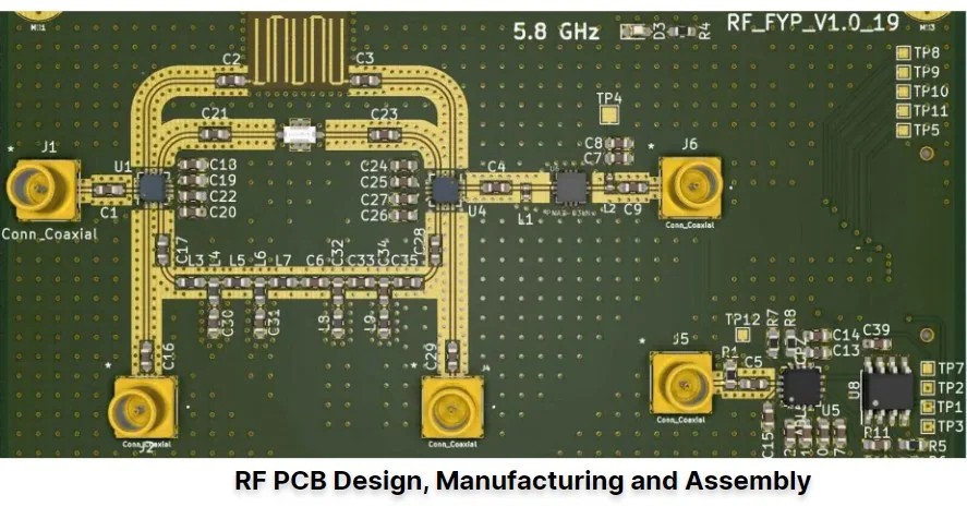
From Design to Manufacturability: Why Fabrication Precision Matters in RF
Impedance Control in Manufacturing: JLCPCB’s Capabilities
A perfectly designed 50Ω trace only delivers 50Ω if the fabrication process is precise enough to realize it. JLCPCB’s controlled impedance service links their online stackup calculator directly to their process parameters, allowing engineers to verify trace widths against the actual manufacturing process before submitting files. Standard tolerance is ±10%, with ±5% available for critical applications, achieved through tight etch control and full-panel AOI inspection.
Reduce Respins: DFM Checks That Catch RF Errors Early
Before production, verify etch factor compensation (Gerbers must account for chemical undercut), drill accuracy for vias down to 0.15 mm, and surface finish selection. For RF work, ENIG is the correct finish, as it provides a flat, non-magnetic surface that avoids the skin-effect losses and permeability issues associated with HASL. Catching these details in DFM review costs nothing; catching them after a first build costs a full respin.
Conclusion: RF PCB Layout
The key to RF PCB design is to consider the board as an active element in the circuit, not a printed circuit board. Keep your impedances at 50Ω, preserve your return paths, design your vias and connectors, keep your RF and digital sections separate, and use the right materials for your frequency of operation.
The final step to close the loop in the design is to produce a board that works in production — almost always at the manufacturing stage — and it’s why you need to work with a precision manufacturer like JLCPCB, which has actual controlled-impedance capability.
FAQ about RF PCB Layout
Q: How do digital harmonics interfere with RF receivers?
Fast digital switching edges produce harmonics that extend into the GHz range. If you are clocking with a 100 MHz clock, the 21st harmonic is 2.1 GHz — right in the LTE receive band. If the trace isn’t kept away from the RF front-end, the harmonic will couple into the LNA and increase the noise floor to the point where weak signals are obscured.
Q: Why is FR-4 unsuitable above 5 GHz?
Two reasons: its dissipation factor converts signal energy to heat at a rate that becomes prohibitive above 5 GHz, and its dielectric constant varies enough batch-to-batch that maintaining precise 50Ω across a production run becomes essentially impossible.
Q: What are via stubs, and why do they cause problems?
A via stub is the unused copper barrel that extends past the target connection layer. It acts as an open-ended transmission line, resonating at specific frequencies and creating sharp notches in the transmission spectrum, where the signal is nearly completely attenuated.
Q: How does a tapered SMA launch improve performance?
The SMA pad is wider than a 50Ω trace, creating an abrupt capacitive step. Tapering the trace width gradually from the pad to the standard route smooths the impedance transition, reducing reflections across the full operating band.
Keep Learning
RF PCB Layout: Common Design Mistakes and Practical Guidelines
Key Takeaways Impedance control is non-negotiable: Maintain consistent 50Ω impedance across all transitions, including vias, connector launches, and trace bends, to prevent reflections and signal loss. Return path integrity determines RF success: Never route RF traces over ground plane splits or slots. Provide continuous return paths with stitch vias at every layer change. Functional zoning prevents interference: Physically separate RF front-end circuitry from digital logic and power management to kee......
High Speed PCB Layout Guide for Reliable Signal Control
High speed PCB routing refers to a layout design where signal behavior follows transmission line theory. High-speed PCB layout treats traces as controlled impedance paths rather than simple conductors. Signal integrity, power integrity, and electromagnetic effects guide routing decisions in high-speed PCB design. Traditional PCB routing focuses on electrical connectivity between components. High-speed PCB layout focuses on waveform preservation, timing accuracy, and noise control. Signal edges propaga......
Signal Integrity Fundamentals in PCB Layout
In the world of PCB design, signal integrity plays a crucial role in ensuring the reliable and accurate transfer of electronic signals. Understanding the fundamentals of signal integrity is essential for electronics enthusiasts, hobbyists, engineers, students, and professionals involved in PCB design. This article will delve into the key concepts of signal integrity and explore how they influence PCB layout. By following best practices, you can optimize signal integrity and enhance the overall perform......
Microstrip v/s Stripline: Layout Difference and When to Use Them
RF (Radio Frequency) PCB design is where engineering meets art. Among the tools in an RF designer's toolkit, microstrip and stripline transmission lines are the unsung heroes. They ensure signals travel seamlessly across PCBs without succumbing to interference, loss, or impedance mismatches. But what are these lines, and how do you choose between them? Let's dive in, and to know more about PCB, see our detailed blog on PCB manufacturing. What Are Microstrip and Stripline Transmission Lines? Microstrip......
IC Board Design: A Technical Guide to PCB Layout
Why is PCB layout so important for an IC board design? PCB layout is the crucial moment when we turn the theoretical elegance of a schematic into a piece of hardware that works reliably and can be manufactured. For any complex board with a complex integrated circuit (IC), such as a microcontroller, an accelerator like an FPGA, or a sensitive RF transceiver, we are not simply connecting one point to another. PCB layout is an engineering specialty that has a huge influence on the performance, signal int......