High-Speed PCB Routing: Guidelines, Techniques & Examples
15 min
- Introduction
- What Is High-Speed PCB Routing?
- High-Speed PCB Routing Guidelines
- Critical Nets Prioritization Rules
- High-Speed PCB Layout Techniques
- High-Speed PCB Routing Example: DDR4 Interface
- Common High-Speed PCB Routing Mistakes
- High-Speed PCB Routing Checklist
- FAQs about High-Speed PCB Routing
Key Takeaways
1. Define "High-Speed" by Rise Time, Not Clock Frequency. Per IPC-2251, traces longer than 2 x rise_time require controlled impedance routing. Even sub-100 MHz signals with fast edges demand transmission-line treatment.
2. Plan the Stackup Before Routing. Every high-speed signal needs an uninterrupted reference plane. Use the fabricator's actual impedance data—JLCPCB guarantees ±10% tolerance on controlled impedance.
3. Route Critical Nets in Priority Order. Route clocks, differential pairs, and DDR memory buses first, then RF lines and analog references. Low-speed GPIO and control nets go last.
4. Maintain Continuous Return Paths and Apply the 3W Rule. Never route across split planes or voids, and keep at least 3x trace-width spacing between signals. Insert ground stitching vias at every layer transition.
5. Keep Differential Pairs Perfectly Symmetric. Constant trace spacing, identical geometry, and equal electrical lengths are non-negotiable. Never place vias on only one pair member.
6. Use Serpentine Routing Only When Timing Demands It. Add tuning only where skew budgets require it, and place serpentines near the receiver. Maintain 3W spacing between adjacent segments.
7. Verify Thoroughly Before Fabrication Release. Complete DRC, signal integrity review, return path inspection, and DFM inspection. A structured constraint-driven workflow improves first-pass success.
Introduction
Modern electronics continue to push data rates higher while shrinking form factors. Whether designing DDR4 memory interfaces, PCIe links, USB 3.x, HDMI, Ethernet, or high-speed ADC/DAC systems, routing quality directly impacts product performance. A well-designed schematic cannot guarantee reliable operation—poor PCB routing can introduce signal integrity (SI) problems, electromagnetic interference (EMI), excessive jitter, timing violations, and manufacturing risks.
Unlike conventional routing, high-speed PCB routing requires engineers to consider electrical behavior throughout the entire physical interconnect. Every trace, via, reference plane, and layer transition influences impedance continuity, return current paths, propagation delay, and crosstalk. As edge rates shrink into the sub-nanosecond range, routing decisions that once seemed insignificant can become the root cause of system instability.
This guide explains the engineering principles behind high-speed PCB routing guidelines, practical layout techniques, common mistakes, and a complete routing example based on real-world high-speed interfaces. It also incorporates key manufacturing data from IPC standards and JLCPCB's production capabilities, ensuring the recommendations are both electrically sound and manufacturable. Whether designing your own board or preparing files for fabrication at JLCPCB, these best practices help achieve better signal integrity, EMI performance, and higher first-pass success. Before ordering, review JLCPCB's ordering instructions to ensure your Gerber files meet all fabrication requirements—including solder mask bridges, plated slot specifications, board outline conventions, and silkscreen design rules.
What Is High-Speed PCB Routing?
High-speed PCB routing treats interconnects as transmission lines rather than ideal conductors. A common rule of thumb for FR-4 microstrip (approximate, non-standard guide): Len(inches) < 2 x rise_time(ns); Traces exceeding this length should be routed with controlled impedance and proper termination.
A common misconception is that "high-speed" is defined solely by clock frequency. In reality, signal rise time is more meaningful—even interfaces below 100 MHz may require controlled impedance routing if edge rates are fast enough. Modern FPGAs, DDR memory, PCIe, USB 3.x, HDMI, and Gigabit Ethernet all fall into this category.
High-speed PCB layout focuses on maintaining predictable electrical characteristics throughout the signal path, simultaneously controlling: characteristic impedance, return current continuity, differential pair coupling, timing skew, crosstalk, reflection, EMI/EMC performance, and manufacturability. Instead of routing each signal independently, engineers treat the PCB as an integrated electromagnetic system where every routing decision influences neighboring signals. Even minor discontinuities—unnecessary vias, split reference planes, or inconsistent differential spacing—can increase insertion loss, degrade eye diagrams, or reduce timing margin.
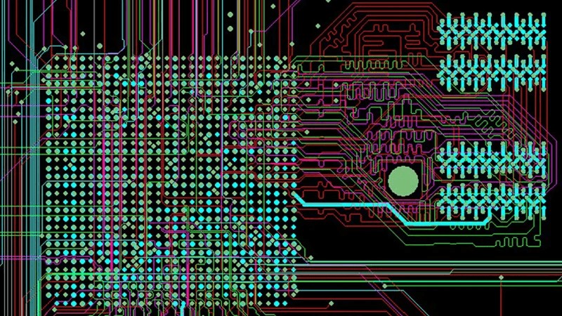
PCB layout design with complex circuit traces.
High-Speed PCB Routing Guidelines
Professional PCB designers adopt a constraint-driven methodology that defines electrical, physical, and manufacturing requirements before routing begins. Every routing decision should satisfy four objectives: Signal Integrity (SI), Power Integrity (PI), Electromagnetic Compatibility (EMC), and Design for Manufacturability (DFM).
High-Speed PCB Constraints & Workflow
A typical engineering workflow consists of four stages:
-
Define Design Constraints
Establish target impedance (50 Ω single-ended, 90 Ω or 100 Ω differential), differential pair spacing, skew budgets, trace width/clearance, length-matching tolerances, via restrictions, and manufacturing limitations. Implement these in PCB design software such as EasyEDA Pro, Altium Designer, or Cadence Allegro.
-
Optimize Component Placement
Position critical devices to minimize high-speed interconnect lengths while preserving continuous return paths. Memory interfaces should reduce bus skew; high-speed connectors should align with signal flow; decoupling capacitors should sit adjacent to power pins.
-
Execute Constraint-Driven Routing
Route critical clocks, differential pairs, memory buses, and RF signals first. Less sensitive control signals and GPIO traces are completed later without disturbing critical channels. Continuously monitor impedance continuity, return paths, layer transitions, spacing, and timing constraints.
-
Verification Before Release
Complete DRC, signal integrity review, length matching verification, return path inspection, differential pair consistency, impedance review, and manufacturing DFM inspection before generating fabrication data.
High-Speed Layer Stackup & Impedance Planning
Stackup planning forms the electrical foundation of every high-speed layout. The primary objective is to provide every high-speed signal with a continuous reference plane while maintaining stable characteristic impedance. JLCPCB supports 1–32 layer PCBs with controlled impedance options from 4 layers and above, using FR-4 laminates from suppliers including Nan Ya, KB, and Shengyi.
A typical four-layer stackup: Top Signal, Solid Ground Plane, Power Plane, Bottom Signal. More complex DDR4, PCIe Gen4/Gen5, or multi-gigabit systems commonly require six or more layers for dedicated reference planes, controlled impedance routing, and improved EMI performance.
Key stackup principles: signal layers should reference uninterrupted ground planes; power and ground planes should be closely coupled; layer transitions must preserve return current continuity; stackup symmetry reduces board warpage. On standard FR4 laminates, the fiber weave effect (glass Dk≈6 vs. resin Dk≈3) can cause intra-pair skew at multi-Gbps rates—using spread glass or routing at an angle mitigates this per IPC-2141A.
Impedance targets are determined during stackup planning. Trace width, dielectric thickness, copper weight, and laminate Dk collectively determine impedance. Because manufacturing tolerances directly affect accuracy, use the fabricator's exact parameters. JLCPCB's free online Impedance Calculator provides real-world substrate Dk and prepreg thickness data, eliminating late-stage revisions. Its controlled impedance tolerance is ±10% for production.
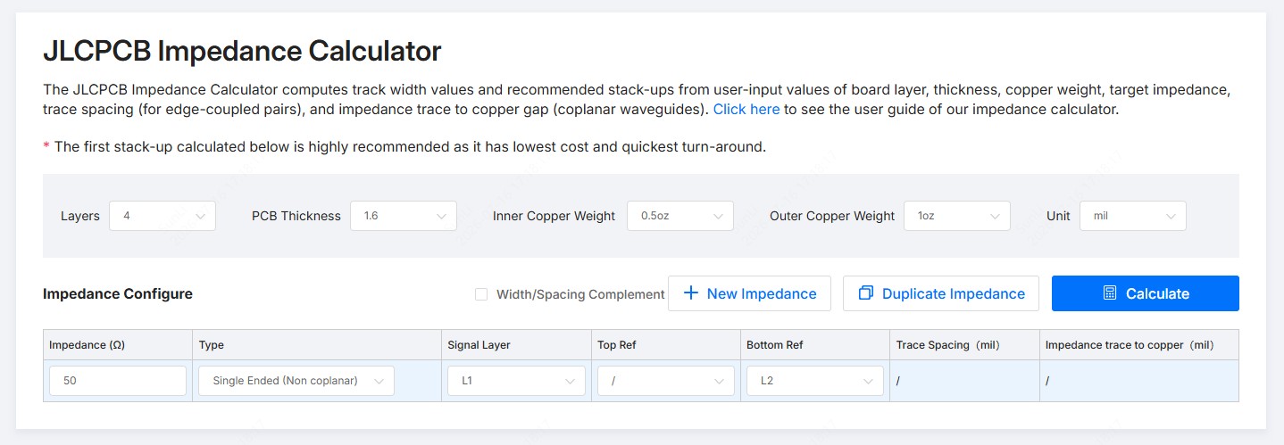
JLCPCB impedance calculator tool online interface.
Critical Nets Prioritization Rules
Not every signal deserves the same routing priority. One of the most important high-speed PCB design rules is identifying critical nets before routing starts—these signals are the most sensitive to impedance discontinuities, timing mismatch, and electromagnetic interference.
A common priority order is:
- Clock signals
- Differential pairs (PCIe, USB, Ethernet, HDMI)
- DDR memory buses
- RF transmission lines
- Analog reference signals
- Remaining digital signals
- Low-speed GPIO and control nets
Clock networks receive highest priority because timing errors propagate system-wide. Differential pairs require consistent spacing, using tight coupling where routing density is limited or loose coupling with controlled spacing, which is common for modern multi-Gbps serial interfaces.
Continuous Return Paths & Crosstalk Prevention
Every signal current forms a complete loop—while the signal travels along the trace, its return current flows through the nearest reference plane. If interrupted by split planes, voids, or unnecessary layer transitions, the current detours around the discontinuity, increasing loop inductance, radiation, and signal distortion. Best practices: route high-speed signals over uninterrupted solid ground planes; avoid crossing plane splits; minimize reference plane changes; keep signal and return paths closely coupled.
The 3W Rule—maintaining spacing of at least three times the trace width between adjacent single-ended traces—significantly reduces capacitive and inductive coupling. For extremely high-speed interfaces (PCIe Gen5, USB4, DDR5), verify spacing using SI simulation rather than empirical rules alone.
JLCPCB DFM Note
When manufacturing at JLCPCB, ensure your design meets these key capabilities:
- 1–2 layer PCBs (1 oz outer copper) support minimum trace width/spacing of 0.10 mm (4 mil)
- 4–32 layer PCBs support 0.09 mm (3.5 mil); BGA fan-out regions can go down to 0.076 mm (3 mil)
- For 2 oz copper, minimum trace/spacing is 0.16 mm (6.5 mil) on 2-layer and 0.15 mm (6 mil) on multilayer
- Minimum via hole size is 0.15 mm with a 0.25 mm outer diameter for multi-layer boards. The production tolerance requires the PTH pad annular ring to be ≥0.15 mm for advanced multi-layer designs (≥0.20 mm recommended for optimal yield)
- Solder mask bridge minimum is 0.10 mm for green and 0.13 mm for black/white
For complete specifications, refer to JLCPCB PCB Capabilities.
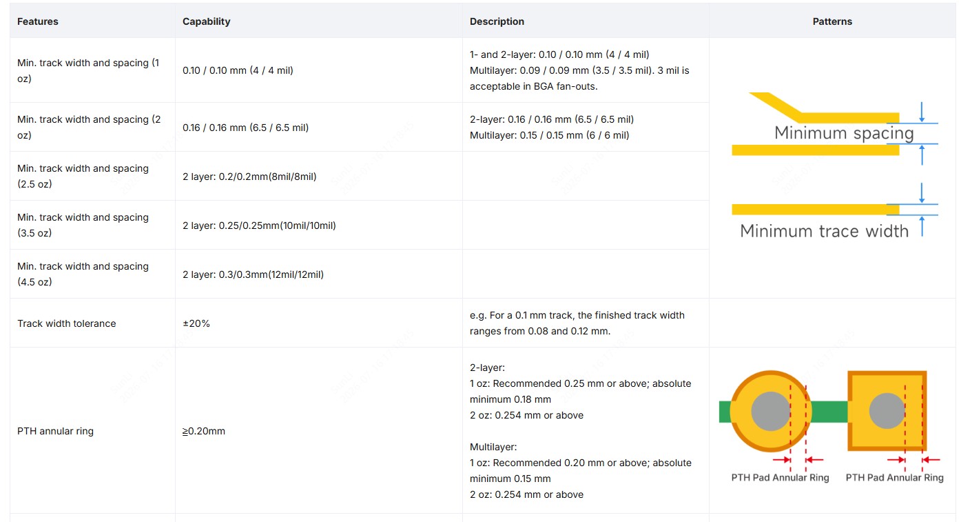
PCB manufacturing capabilities showing minimum track width, spacing limits, and PTH annular ring sizes.
High-Speed PCB Layout Techniques
Differential Pair & Controlled Impedance Routing
Differential signaling is standard for modern high-speed interfaces due to excellent noise immunity and lower EMI compared to single-ended routing. Successful differential routing depends on constant trace spacing, identical trace geometry, symmetrical layer transitions, equal electrical lengths, and continuous reference planes.
Any sudden spacing variation changes differential impedance, causing reflections and increasing mode conversion. Avoid placing vias on only one member of a differential pair; if both traces must change layers, they should transition together using identical via structures.
While 90° corners are acceptable below ~10 GHz on typical trace widths, 45° bends or smooth arcs are industry-preferred for maintaining impedance continuity. Manufacturing tolerances—dielectric thickness, copper weight, etching compensation, and laminate material—must be considered early with the fabricator to ensure consistent impedance production.
Serpentine Routing & Timing Matching
Length matching satisfies timing constraints rather than equalizing physical lengths. Within DDR memory buses, high-speed parallel interfaces, and certain differential pairs, signals must arrive within a specified skew budget. When natural routing differences exceed the allowable timing window, serpentine routing adds delay.
Best practices: add tuning only where required; place near the receiver whenever practical; use smooth, evenly spaced serpentine segments; follow 3W spacing between adjacent segments; avoid tightly packed meanders that increase self-coupling.
Overusing serpentine routing can actually increase delay uncertainty—satisfy the minimum required length rather than adding unnecessary tuning. For DDR4, byte lanes often require data signals matched within tens of mils, while address/command buses follow separate timing budgets defined by the memory topology.
Clock Routing Best Practices
Clock signals establish the timing reference for the entire digital system. Any degradation in clock quality directly affects setup time, hold time, synchronization, and overall system reliability. Key practices: keep clock traces as short as practical, minimize via count, maintain continuous reference planes, avoid routing near switching power supplies, isolate clocks from noisy parallel buses, and maintain adequate spacing from other high-speed signals. For multiple clock destinations, matched electrical lengths reduce skew; excessive branching should be avoided unless required by the clock distribution architecture. Differential clock routing must preserve pair symmetry throughout every bend and layer transition.
Layer Transitions, Via Stitching & Reference Management
Each via introduces parasitic inductance, capacitance, and impedance discontinuities. Reduce unnecessary layer transitions—keep critical signals on a single layer when possible. When layer changes are required: transition both differential traces together, minimize via stubs, consider back-drilling for very high-speed interfaces, and use ground stitching vias adjacent to signal vias for a short return path between reference planes. As signaling speeds increase into the multi-gigabit range, via optimization becomes as important as trace routing itself.
High-Speed PCB Routing Example: DDR4 Interface
This example demonstrates a DDR4 memory interface at 2400 MT/s on a six-layer PCB, representative of many high-speed digital system workflows.
Stackup & Impedance Targets
A symmetrical six-layer stackup (SIG/GND/PWR/SIG/GND/SIG) ensures every high-speed routing layer has an adjacent reference plane. Impedance targets: single-ended DDR signals (including address, command, and data DQ buses) are set to 50 Ω, and the differential clock pair is configured for 100 Ω. Trace widths and spacing are calculated using the manufacturer's impedance tables, not generic field-solver assumptions.
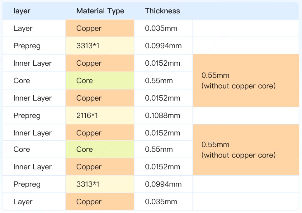
6-layer PCB stackup structure chart detailing copper thickness, prepreg types, and core dimensions.
Routing Strategy
Step 1 – Route the clock network first. The differential clock pair is routed before all other memory signals on a single layer, with no unnecessary vias, over continuous ground, with constant differential spacing.
Step 2 – Route address and command signals. DDR4 uses fly-by topology; signals pass sequentially from one device to the next. Branch lengths are minimized, reference planes remain continuous.
Step 3 – Route data byte lanes. Each byte lane (DQ signals + DQS differential pair + DM signal) is treated as a routing group. Within each lane, DQ traces match electrical length, DQS pairs maintain constant spacing, crosstalk between neighboring lanes is reduced.
Step 4 – Maintain return path integrity. Ground stitching vias are inserted at every layer transition. Return-current discontinuities are minimized.
Step 5 – Complete remaining signals. Lower-speed control nets are routed without disturbing optimized high-speed channels.
After routing, the design undergoes DRC verification, signal integrity review, timing optimization, and manufacturability review before fabrication data is released. The final design demonstrates controlled impedance across all critical signal paths, stable differential pair coupling, continuous return current paths on every routing layer, length matching within specified timing budgets, minimal EMI through reduced loop area, and manufacturing-ready geometry verified by DRC and DFM review. This structured engineering process—from constraints through disciplined routing to comprehensive verification—significantly improves first-pass success while reducing costly PCB revisions.
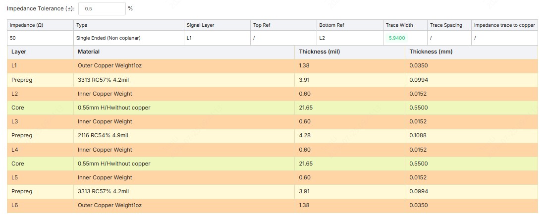
Calculate 50 ohm single-ended microstrip trace width for 6-layer PCBs using JLCPCB stackup.
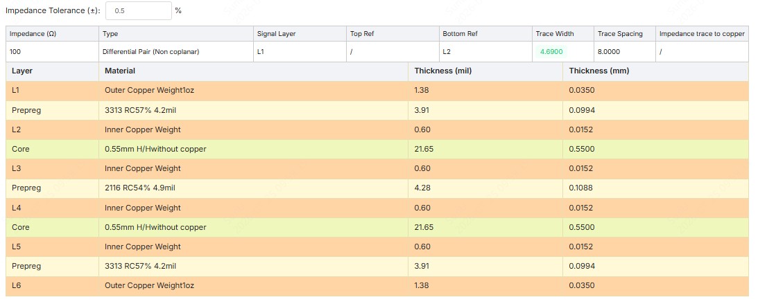
Calculate 100 ohm differential pair trace width and spacing for 6-layer PCBs on JLCPCB.
Common High-Speed PCB Routing Mistakes
Mistakes to Avoid
- Broken Return Paths. Routing across split ground planes or large voids forces return currents to detour, increasing loop inductance and EMI. Always verify continuous reference planes beneath every critical signal.
- Excessive Layer Transitions. Every via adds parasitic inductance and capacitance. Keep critical signals on a single layer, transition differential pairs together, minimize via stubs, and consider back-drilling for multi-gigabit designs.
- Poor Differential Pair Routing. Inconsistent spacing, unmatched via counts, asymmetric bends, and abrupt spacing changes alter differential impedance and increase mode conversion. Treat differential pairs as one transmission structure throughout.
- Routing Across Split Reference Planes. Crossing power-plane splits interrupts return paths even if the trace appears continuous. Redesign the stackup or provide ground stitching vias for an alternative low-inductance return path.
- Ignoring Length Matching. Skew requirements on DDR interfaces and parallel buses are critical. Ignoring them may reduce setup/hold margins enough to cause intermittent failures. Conversely, excessive serpentine routing degrades signal quality through self-coupling.
High-Speed PCB Routing Checklist
1Stackup & Impedance
- PCB stackup matches impedance calculation; controlled impedance traces use correct width and spacing
- Signal layers reference continuous ground planes; manufacturing tolerances have been considered
- Fabrication notes clearly specify impedance requirements
2Critical Signal Review
- Clock signals, DDR buses, PCIe lanes, USB differential pairs, Ethernet, and RF lines satisfy routing priority, impedance, spacing, skew, and via constraints
3Return Path Verification
- Uninterrupted reference planes, proper return current continuity, minimal loop area, correctly placed ground stitching vias, no routing across plane splits
4DFM Verification
- DRC passes without violations; copper spacing satisfies fabrication capability; via sizes meet manufacturing requirements; copper balance is acceptable; differential pair geometry is consistent; silkscreen and solder mask clearances are correct; Gerber files pass DFM inspection
FAQs about High-Speed PCB Routing
Q: What is considered high-speed PCB routing?
High-speed PCB routing refers to layout where transmission line effects become significant. Designers must control impedance, return current paths, timing, and electromagnetic coupling. Interfaces such as DDR4/DDR5, PCIe, USB 3.x, HDMI, SATA, and Gigabit Ethernet all require high-speed routing techniques.
Q: What are the most important high-speed PCB routing guidelines?
Plan the PCB stackup before routing; route critical nets first; maintain continuous reference planes; control impedance throughout the signal path; keep differential pairs tightly coupled; minimize vias and layer transitions; match lengths only where timing requires; verify the design using DRC, SI, and DFM reviews.
Q: Why is controlled impedance important?
When impedance changes along a transmission path, part of the signal energy reflects back toward the source, distorting waveforms, reducing eye openings, increasing jitter, and causing communication errors. Consistent impedance improves signal integrity and reduces design iterations.
Q: When should serpentine routing be used?
Only when signals must satisfy specific timing constraints, such as DDR memory buses or parallel interfaces. It is not intended to make every trace equal length. Excessive serpentine routing introduces self-coupling and additional delay uncertainty.
Conclusion: High-Speed PCB Routing
Successful high-speed PCB routing is built on engineering discipline rather than isolated techniques. Every design decision—from stackup planning and impedance control to differential pair routing, return path management, and timing verification—contributes to overall signal integrity and system reliability. Following proven guidelines enables engineers to minimize reflections, crosstalk, EMI, and timing violations while improving manufacturability. Just as importantly, adopting a constraint-driven workflow ensures that routing decisions remain consistent from initial placement through final DRC, SI, and DFM verification. Whether developing DDR memory interfaces, PCIe links, USB, Ethernet, or other high-speed digital systems, applying these techniques produces robust, production-ready designs with fewer prototype iterations and higher first-pass success.
Keep Learning
SFP Pinout Explained: PCB Layout & Design Guide
Key Takeaways The SFP pinout follows a standard 20-pin edge connector, with dedicated pins for power, ground, differential data pairs, and I2C control signals. The Tx and Rx differential pairs carry the high-speed optical or copper signal and need controlled 100 ohm differential impedance through the entire routing path. Low-speed control pins (TX_FAULT, TX_DISABLE, MOD_ABS, LOS, Rate Select/RS1) use standard single-ended routing and don't need impedance matching. Placing the SFP cage near the board e......
HDMI PCB Layout Guidelines:Impedance & Length Matching
Key Takeaways Route the four TMDS pairs as 100 Ω differential pairs, and hold that value through vias, pads, and the connector. Match the P and N traces in each pair first, then match the pairs to each other within your silicon vendor's limits. Keep a solid reference plane under the whole route. Never cross a split. Put ESD protection as close to the connector as practical, so surge current is diverted early. Check the signaling type first. TMDS matching rules do not apply to HDMI 2.1 FRL. Introductio......
RGMII Routing Guidelines for Reliable Gigabit PCB Design
Key Takeaways RGMII is a 12-signal, single-ended, source-synchronous parallel interface; its TX and RX paths are separate timing groups. Match TXD[3:0] and TX_CTL to TXC. Match RXD[3:0] and RX_CTL to RXC. Do not match TX against RX. Budget the aggregate clock-to-data skew separately in each direction, and avoid unintentionally stacking a full PCB delay with an enabled silicon delay. Treat 50 Ω ±10%, 20 mil matching and a 6 inch route limit as TI layout guidance, not universal clauses of the RGMII spec......
Ethernet PCB Routing: Guidelines for MAC, PHY, and RJ45
Key Takeaways Route every MDI pair as a 100 Ω differential transmission line with ±10% control, unless the selected PHY or cable specification requires a different target. TI recommends keeping each MDI route below 2 in and matching P to N within 20 mil for 1 Gb/s or 50 mil for 10/100 Mb/s. Keep metal out from under discrete magnetics, separate chassis ground from board ground, and preserve a continuous reference beneath the routed pairs. TI’s Ethernet-specific guidance places suitable ESD protection ......
DDR5 PCB Layout Guidelines: Design Rules and Best Practices
Key Takeaways DDR5 raises the stakes on layout: 1.1V rails and data rates up to 8800 MT/s leave far less margin for error than DDR4 did. Target around 40–45 Ω single-ended for DQ/CA and 80 Ω differential for CLK/DQS — exact values come from vendor guidelines — and hold them through every via and connector. Keep DQ and DQS length matching within about 5 mil per byte lane, and never route a DDR5 signal over a gap in its reference plane. Plan for 8 to 12 layers with dedicated ground references next to ev......
Via Stitching in PCB Design: A Complete Guide
Key Takeaways Via stitching bonds same-net copper across layers with repeated plated vias, most often ground, to cut high-frequency impedance between regions. A grounded via next to a signal layer transition gives return current a short local path and helps confine the field around the via. Via fences along board edges and RF cavities suppress edge radiation, but their isolation is geometry- and frequency-dependent, with no universal dB value. Keep stitching pitch at or below one-twentieth of the in-b......