PCIe Pinout: A Complete Pin Reference From x1 to x16
18 min
- Introduction
- PCIe Slot Pinout: The Complete Pin Table From x1 to x16
- PCIe Slot and Card-Edge Basics: Keying and Orientation
- PCIe Slot Power Pins: +12V, +3.3V, and +3.3Vaux
- Sideband and Control Signals Explained
- Common PCIe Pinout and Wiring Mistakes
- From Pinout to Layout
- FAQs About PCIe Pinout
- Conclusion About PCIe Pinout
PCIe Pinout Quick Reference
- x1: 36 contacts, 18 per side.
- x4: 64 contacts, 32 per side.
- x8: 98 contacts, 49 per side.
- x16: 164 contacts, 82 per side.
- Contact pitch: 1.0 mm; A is the solder face, B the component face.
- Max slot power: 75 W for a standard-height x16 card after configuration (25 W at power-up); x4/x8: 25 W.

Introduction
You are designing an add-in card, with the controller symbol on one side of the screen and the gold-finger footprint on the other. The PCIe pinout defines which physical contact carries each supply, data pair and control signal. Reverse the connector view, or connect a transmitter to another transmitter, and the card may never enumerate.
This PCI Express pinout reference starts with the complete x1 map and adds only the contacts needed for wider connectors. It then separates slot power from startup limits, explains the sidebands, and identifies the checks that matter when the schematic becomes a layout. The tables use an explicitly identified CEM revision rather than treating every generation as identical.
PCIe Slot Pinout: The Complete Pin Table From x1 to x16
The PCIe pinout below uses CEM 5.0, Table 6-1 as its baseline, as listed in the PCI-SIG CEM specification revision index. CEM naming follows the system board: PET pairs carry host TX to card RX; PER pairs carry card TX to host RX.
Wider connectors extend the lane blocks and distributed grounds beyond the x1 base. Their far-end PRSNT2# positions provide the card’s presence-loop connection, not its negotiated lane count. An x1 card can up-plug into a wider supported slot and operate as x1; the connector’s mechanical size alone does not establish electrical width.
| Width | Contacts per Side | Total Contacts |
|---|---|---|
| x1 | 18 | 36 |
| x4 | 32 | 64 |
| x8 | 49 | 98 |
| x16 | 82 | 164 |
The four tables together define every contact; extension tables do not repeat earlier rows. p and n mean positive and negative, # marks an active-low signal, and RSVD means reserved. Do not assign a new function to a reserved contact.
PCIe x1 Pinout (Pins 1-18)
| Pin | Side B | Side A | Description |
|---|---|---|---|
| 1 | +12V | PRSNT1# | B: +12 V; A: presence-loop start |
| 2 | +12V | +12V | +12 V on both faces |
| 3 | +12V | +12V | +12 V on both faces |
| 4 | GND | GND | Ground returns |
| 5 | SMBCLK (SMCLK) | JTAG2 (TCK) | SMBus clock; JTAG clock input |
| 6 | SMBDAT (SMDAT) | JTAG3 (TDI) | SMBus data; JTAG data input |
| 7 | GND | JTAG4 (TDO) | Ground; JTAG data output |
| 8 | +3.3V | JTAG5 (TMS) | Main +3.3 V; JTAG mode select |
| 9 | JTAG1 (TRST#) | +3.3V | JTAG reset; main +3.3 V |
| 10 | +3.3Vaux | +3.3V | Auxiliary +3.3 V; main +3.3 V |
| 11 | WAKE# | PERST# | Card wake; host fundamental reset |
| 12 | CLKREQ# | GND | Clock request; ground |
| 13 | GND | REFCLK+ | Ground; reference-clock positive |
| 14 | PETp0 | REFCLK- | Host TX0+ to card RX; REFCLK− |
| 15 | PETn0 | GND | Host TX0− to card RX; ground |
| 16 | GND | PERp0 | Ground; card TX0+ to host RX |
| 17 | PRSNT2# | PERn0 | x1 presence endpoint; card TX0− |
| 18 | GND | GND | Ground returns |
Read each row as a matched pair of contact numbers: row 1 means B1 and A1, not two interchangeable pins. Pin 1 is at the bracket/I/O-panel end of the standard card-edge drawing. Side B is the primary/component face; Side A is the secondary/solder face. Looking at the opposite face mirrors the appearance, not the electrical numbering.
For this PCIe pinout, the presence trace runs from A1, PRSNT1#, to B17, PRSNT2#, on an x1 card. Wider cards use B31, B48 or B81 at their far end. Keep the other prescribed contacts physically present even when their functions are unused.
Presence and training are separate. The loop tells the host that a card is present; CEM 5.0 ties the host’s PRSNT2# positions together, so that circuit is not a standardized physical-size detector. The operating lane count is negotiated during link training, not read from PRSNT#.
Older CEM revisions used shorter PRSNT contacts for last-mate/first-break detection, and most public pin tables still show that arrangement. CEM 5.0 and later specify managed-only hot plug for cards up to 75 W, while finger-length rules are revision-specific: confirm the mechanical chapter of your target CEM revision rather than assuming one rule for every generation.
PCIe x4 Pinout (Pins 19-32)
Pins 1–18 remain as defined above; the following rows add lanes 1–3 and the x4 end-position presence contact.
| Pin | Side B | Side A | Description |
|---|---|---|---|
| 19 | PETp1 | MFG | B: host TX1+ to card RX; A: manufacturing test |
| 20 | PETn1 | GND | B: host TX1− to card RX; A: ground |
| 21 | GND | PERp1 | B: ground; A: card TX1+ to host RX |
| 22 | GND | PERn1 | B: ground; A: card TX1− to host RX |
| 23 | PETp2 | GND | B: host TX2+ to card RX; A: ground |
| 24 | PETn2 | GND | B: host TX2− to card RX; A: ground |
| 25 | GND | PERp2 | B: ground; A: card TX2+ to host RX |
| 26 | GND | PERn2 | B: ground; A: card TX2− to host RX |
| 27 | PETp3 | GND | B: host TX3+ to card RX; A: ground |
| 28 | PETn3 | GND | B: host TX3− to card RX; A: ground |
| 29 | GND | PERp3 | B: ground; A: card TX3+ to host RX |
| 30 | PWRBRK# | PERn3 | B: emergency power reduction; A: card TX3− to host RX |
| 31 | PRSNT2# | GND | B: presence endpoint; A: ground |
| 32 | GND | RSVD | B: ground; A: reserved |
A19 is MFG in this CEM 5.0 map; older charts may show it reserved. B30 is PWRBRK#, not a spare GPIO. M.2 uses a different connector specification and its own assignments; it is outside this reference.
PCIe x8 Pinout (Pins 33-49)
Add these rows to the x1 and x4 tables. They provide lanes 4–7 and the x8 presence-loop endpoint at B48.
| Pin | Side B | Side A | Description |
|---|---|---|---|
| 33 | PETp4 | RSVD | B: host TX4+ to card RX; A: reserved |
| 34 | PETn4 | GND | B: host TX4− to card RX; A: ground |
| 35 | GND | PERp4 | B: ground; A: card TX4+ to host RX |
| 36 | GND | PERn4 | B: ground; A: card TX4− to host RX |
| 37 | PETp5 | GND | B: host TX5+ to card RX; A: ground |
| 38 | PETn5 | GND | B: host TX5− to card RX; A: ground |
| 39 | GND | PERp5 | B: ground; A: card TX5+ to host RX |
| 40 | GND | PERn5 | B: ground; A: card TX5− to host RX |
| 41 | PETp6 | GND | B: host TX6+ to card RX; A: ground |
| 42 | PETn6 | GND | B: host TX6− to card RX; A: ground |
| 43 | GND | PERp6 | B: ground; A: card TX6+ to host RX |
| 44 | GND | PERn6 | B: ground; A: card TX6− to host RX |
| 45 | PETp7 | GND | B: host TX7+ to card RX; A: ground |
| 46 | PETn7 | GND | B: host TX7− to card RX; A: ground |
| 47 | GND | PERp7 | B: ground; A: card TX7+ to host RX |
| 48 | PRSNT2# | PERn7 | B: presence endpoint; A: card TX7− to host RX |
| 49 | GND | GND | B: ground; A: ground |
Do not renumber the extended region from one when creating the footprint. A33 and B33 remain distinct contacts with different functions, and the ground positions are part of the defined connector—not optional filler around the data pins.
PCIe x16 Pinout (Pins 50-82)
Add these rows after the x8 extension for lanes 8–15 and the x16 presence-loop endpoint at B81.
| Pin | Side B | Side A | Description |
|---|---|---|---|
| 50 | PETp8 | RSVD | B: host TX8+ to card RX; A: reserved |
| 51 | PETn8 | GND | B: host TX8− to card RX; A: ground |
| 52 | GND | PERp8 | B: ground; A: card TX8+ to host RX |
| 53 | GND | PERn8 | B: ground; A: card TX8− to host RX |
| 54 | PETp9 | GND | B: host TX9+ to card RX; A: ground |
| 55 | PETn9 | GND | B: host TX9− to card RX; A: ground |
| 56 | GND | PERp9 | B: ground; A: card TX9+ to host RX |
| 57 | GND | PERn9 | B: ground; A: card TX9− to host RX |
| 58 | PETp10 | GND | B: host TX10+ to card RX; A: ground |
| 59 | PETn10 | GND | B: host TX10− to card RX; A: ground |
| 60 | GND | PERp10 | B: ground; A: card TX10+ to host RX |
| 61 | GND | PERn10 | B: ground; A: card TX10− to host RX |
| 62 | PETp11 | GND | B: host TX11+ to card RX; A: ground |
| 63 | PETn11 | GND | B: host TX11− to card RX; A: ground |
| 64 | GND | PERp11 | B: ground; A: card TX11+ to host RX |
| 65 | GND | PERn11 | B: ground; A: card TX11− to host RX |
| 66 | PETp12 | GND | B: host TX12+ to card RX; A: ground |
| 67 | PETn12 | GND | B: host TX12− to card RX; A: ground |
| 68 | GND | PERp12 | B: ground; A: card TX12+ to host RX |
| 69 | GND | PERn12 | B: ground; A: card TX12− to host RX |
| 70 | PETp13 | GND | B: host TX13+ to card RX; A: ground |
| 71 | PETn13 | GND | B: host TX13− to card RX; A: ground |
| 72 | GND | PERp13 | B: ground; A: card TX13+ to host RX |
| 73 | GND | PERn13 | B: ground; A: card TX13− to host RX |
| 74 | PETp14 | GND | B: host TX14+ to card RX; A: ground |
| 75 | PETn14 | GND | B: host TX14− to card RX; A: ground |
| 76 | GND | PERp14 | B: ground; A: card TX14+ to host RX |
| 77 | GND | PERn14 | B: ground; A: card TX14− to host RX |
| 78 | PETp15 | GND | B: host TX15+ to card RX; A: ground |
| 79 | PETn15 | GND | B: host TX15− to card RX; A: ground |
| 80 | GND | PERp15 | B: ground; A: card TX15+ to host RX |
| 81 | PRSNT2# | PERn15 | B: presence endpoint; A: card TX15− to host RX |
| 82 | RSVD | GND | B: reserved; A: ground |
The x1 base plus the three extension tables reproduce the complete 164-contact CEM 5.0 map. A mechanically x16 card or slot may implement fewer electrical lanes; check the controller connection and platform specification rather than assuming that every visible lane position is active.
PCIe Slot and Card-Edge Basics: Keying and Orientation
The PCIe edge connector pinout and the mating receptacle use corresponding contact numbers, but their drawing views differ. Establish which face you are viewing before copying pad numbers. A footprint shown from the solder side of a motherboard is not automatically the same view as the component face of the card.
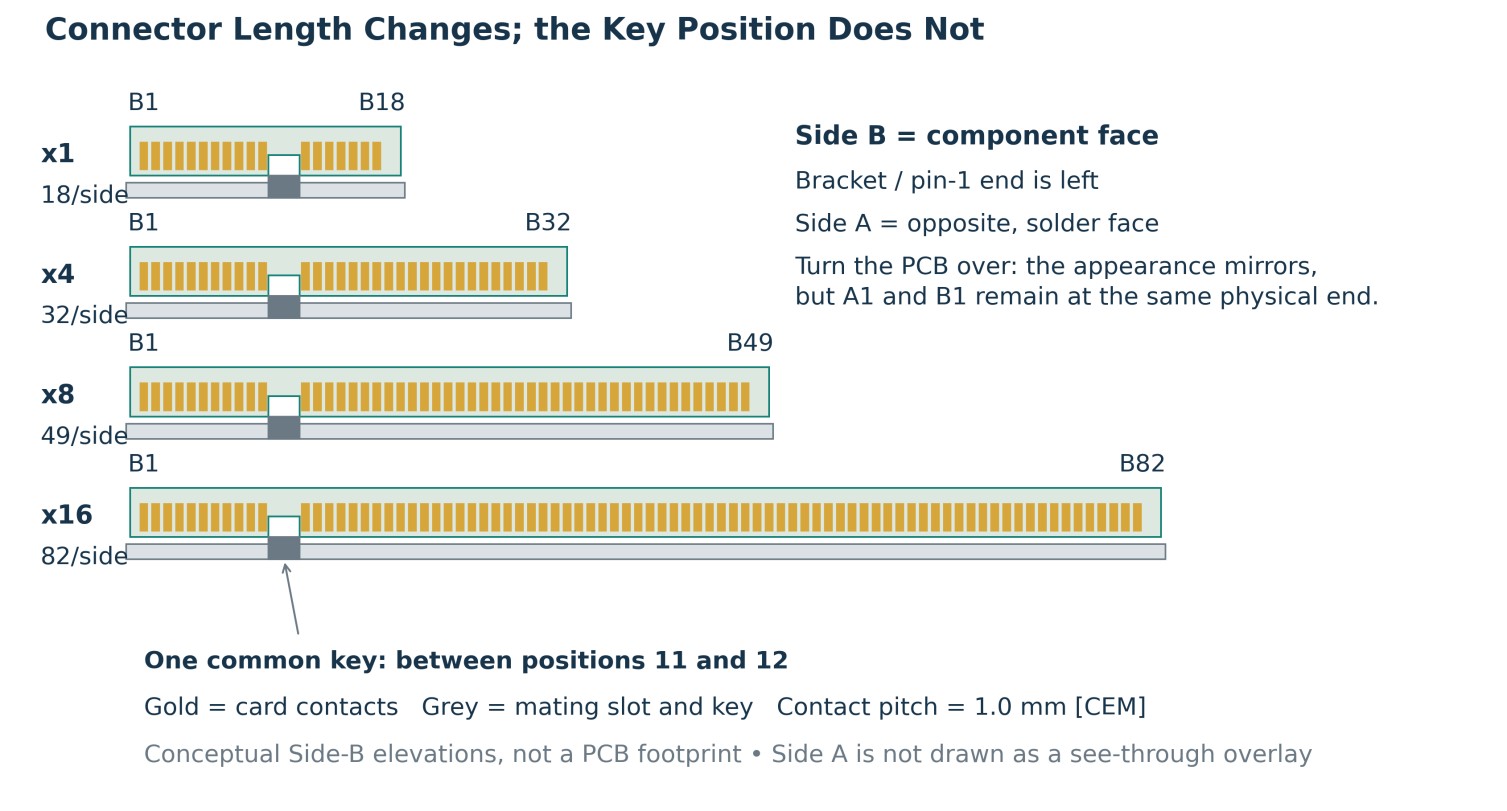
Figure 1. All four connector widths share the key between positions 11 and 12. These are conceptual Side-B elevations with the bracket end to the left; the opposite card face must not be mistaken for a transparent overlay. Not a manufacturing footprint.
The contact pitch is 1.0 mm, and every width places its key between positions 11 and 12. This PCIe pin diagram shows why a narrow card can enter a wider connector: the power/sideband bank and key align before the lane field extends farther along the card. Keying establishes orientation and distinguishes the connector family; it is not a width lock. Legacy PCI is not an interchangeable receptacle.
A closed short slot mechanically blocks a longer card. Some open-ended connectors admit longer cards, but such down-plugging is outside the verified CEM 5.0 scope and does not guarantee platform support. Mini-PCIe is another connector standard with a different map.
The lane, power and ground positions have stayed the same from Gen 1 through Gen 5, and PCIe 6.0 keeps backward compatibility with the same signal assignments. Some reserved sideband contacts were later given functions: B12, A19 and B30 differ between the CEM 3.0 and 5.0 tables. CEM 6.0.1 is a separate revision; its final pin-table and finger-dimension details must be checked against the official CEM 6.0.1 specification record before releasing a Gen 6 footprint. Compatibility does not mean identical copper artwork.
PCIe Slot Power Pins: +12V, +3.3V, and +3.3Vaux
The main +12 V contacts are B1–B3 and A2–A3; main +3.3 V appears at B8, A9 and A10. B10 supplies +3.3Vaux, the auxiliary rail used for supported standby and wake functions when the system provides that power. Do not short it to the main +3.3 V rail merely because their nominal voltages match.
Width alone does not set maximum usable slot power. CEM 5.0 distinguishes initial draw from the maximum allowed after software configuration:
| Card Connector / Physical Class | Initial Edge-Connector Limit | Configured Maximum |
|---|---|---|
| x1, low-profile | 10 W | 10 W |
| x1, half-length | 10 W | 10 W |
| x1, full-length standard-height | 10 W | 25 W |
| x4 | 25 W | 25 W |
| x8 | 25 W | 25 W |
| x16, standard-height graphics card | 25 W | 75 W |
These are CEM 5.0 class limits, not permission to draw the maximum from every socket. +3.3 V is limited to 3 A on every card; at +12 V the published limits are 0.5 A for x1, 2.1 A for x4 and wider, and 5.5 A for a full-sized x16 graphics card after configuration. Verify these figures against the CEM table for your selected revision. Observe the platform’s power allocation, each rail’s current limit, and the combined power ceiling; cooling must also support the card. The contact currents determine the required power-fanout copper and via capacity. Widening that copper does not grant a higher slot power budget.
Cards exceeding the slot power envelope use auxiliary power connectors wired to the system supply; those separate connectors are outside this gold-finger reference.
Sideband and Control Signals Explained
Data pairs cannot compensate for an incorrectly connected control signal. Keep direction relative to the host/card boundary explicit, especially when the controller symbol uses local TX/RX names rather than connector names.
| Signal | Direction | Function |
|---|---|---|
| PERST# — A11 | Host → card | Fundamental reset input to the card |
| REFCLK+/− — A13/A14 | Host → card, standard common-clock slot | 100 MHz differential reference clock |
| CLKREQ# — B12 | Card → host; shared in L1 PM substates | Open-drain clock request and low-power coordination |
| WAKE# — B11 | Card → host | Open-drain request to reactivate the link/system |
| SMBCLK/SMBDAT — B5/B6 | Bidirectional bus; host usually manages it | Optional SMBus management interface |
| TCK, TDI, TMS, TRST# | Host/test interface → card | JTAG clock, data input, mode and reset |
| TDO | Card → host/test interface | JTAG test data output |
| PWRBRK# — B30 | Host → card | Optional emergency power reduction |
| MFG — A19 | Manufacturer-defined; host unconnected | Optional manufacturing test mode |
Directions and functions follow CEM 5.0, Chapter 2 and Table 6-1. In a standard add-in card, PERST# is supplied by the system: adding an RC delay is not a general card requirement. The clock pair supplies a reference, while data timing is recovered by the receiver; clock architecture must match the devices and platform.
CLKREQ# is not exclusively a one-way output in every state: either end may assert it for L1 PM-substate exit. WAKE# and implemented clock-request circuitry need the prescribed open-drain behavior and host-side biasing; do not replace them with unqualified push-pull outputs.
SMBus, JTAG, clock power management and the additional optional controls need not all be implemented by a basic x1 card. If JTAG is implemented, treat its pins as a set. An optional function does not make its physical contact available for repurposing or exempt it from the applicable termination requirements.
Common PCIe Pinout and Wiring Mistakes
- Mirrored footprint. Check A1/B1 against the bracket end and the specified drawing view before assigning the remaining pads. Flipping the PCB view without preserving pad numbers can miswire power as well as signals.
- PET/PER interpreted from the card. In CEM terminology, PET reaches the card receiver and PER leaves the card transmitter. Compare direction at both ends of each pair, not just the letters TX and RX in two symbols.
- Missing presence bridge. Connect A1 to the far-end PRSNT2# position for the card’s mechanical width. Do not confuse physical contact population with the lane width that the controller will negotiate.
- Auxiliary and main rails combined. Keep B10’s +3.3Vaux supply distinct from main +3.3 V. Review standby behavior and prevent unintended back-powering through interface circuitry.
- Asymmetric pair fanout. Avoid giving one conductor a longer escape or an unmatched via detour; use our high-speed PCB routing guidelines for the electrical checks.
- Unimplemented open-drain behavior. Where CLKREQ# or WAKE# is used, verify the required biasing, off-state tolerance and assertion logic at the system boundary. Leaving a used control network undefined can defeat power-state transitions.
- Management or reserved pins treated as spare nets. Implement SMBus if the platform expects it, and leave reserved or unused optional functions in their prescribed state. In particular, do not copy an old reserved label onto a contact assigned a function by the selected revision.
From Pinout to Layout
The differential pairs and REFCLK require controlled-impedance treatment. Use our high-speed PCB routing guidelines for the impedance, matching and skew constraints; this pin reference deliberately does not duplicate their numeric rules.
Make the presence bridge visible in the schematic so it survives into the layout. Size the +12 V and +3.3 V fanout for the permitted current, and preserve a continuous ground return through the connector region. Avoid a broad plane gap beneath the channel; any local launch relief must follow the applicable connector design rather than a generic keep-out rule.
PCIe pin assignment allows supported lane reversal, not arbitrary lane permutation. Base 6.0 still lists lane reversal as optional and requires a consistent mapping in both the transmit and receive directions, as stated in the PCI Express Base Specification overview. For example, a supported reversed lane group is different from swapping isolated middle lanes. Polarity inversion is separate: the receiver must handle an individual pair’s p/n inversion during training. Confirm controller support before changing the logical lane order; training cannot repair an unsupported wiring pattern.
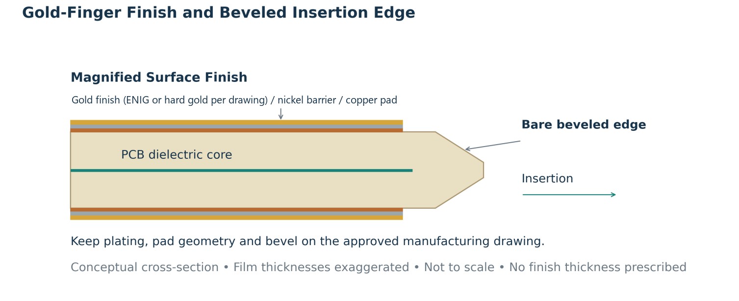
Figure 2. The contact finish and gold-finger bevel serve different purposes. The layer thicknesses are exaggerated and no fabrication dimensions are prescribed; use the applicable CEM drawing and approved finish specification. The gold finish shown is generic — ENIG or electroplated hard gold as specified on the drawing — over a nickel barrier and copper pad; it does not describe any single fabricator’s standard process.
Confirm the required contact plating and bevel against the manufacturing drawing and JLCPCB’s gold-finger capabilities. JLCPCB’s standard gold-finger finish is ENIG, with 30° or 45° bevel options; electroplated hard gold is not offered as a standard finish, so confirm any hard-gold requirement with the fabricator before release. Confirm controlled impedance separately against the stack-up and routing rules.
FAQs About PCIe Pinout
How Many Contacts Does a PCIe x16 Slot Have?
A standard x16 connector has 164 contacts: 82 per side. The PCIe x16 pinout combines the x1 base with three extension tables; mechanical width does not guarantee that every lane is electrically connected.
How Many Contacts Does a PCIe x1 Slot Have?
An x1 connector has 36 contacts: 18 per side. The PCIe x1 pinout includes power, lane zero and control contacts; “x1” is the lane count, not the pin count.
Are Contact Assignments Identical Across Generations?
Mostly, but not identical. The lane, power and ground positions are unchanged, while several sideband contacts gained functions in later CEM revisions. The lane/power arrangement supports compatibility, but the selected CEM revision governs optional functions and mechanics; final CEM 6 details need a revision-specific check.
Will an x1 Card Work in an x16 Slot?
Yes, standard up-plugging allows an x1 card in an appropriate x16 slot, with an x1 link. Confirm the platform supports the device; a wider receptacle does not turn a single-lane controller into a wider one.
What Do PRSNT1# and PRSNT2# Do?
They implement card presence detection, not lane-count negotiation. The card bridges A1 to its far-end PRSNT2#; the standard CEM 5.0 host circuit does not provide independent size sensing at each PRSNT2# position.
What Is the Difference Between PET and PER?
PET is host transmit/card receive; PER is card transmit/host receive. Those names follow the system-board perspective, which is why blindly joining identical TX labels can miswire the card.
What Is PERST# Used For?
PERST# is the card’s fundamental reset input from the host. Implement it as the platform and controller require; an arbitrary RC delay is not part of the standard edge-pin assignment.
Conclusion About PCIe Pinout
A dependable PCIe pinout reference must identify its revision and its viewing direction. The x1 base and three extension tables above cover all contacts through x16, while keeping the system-board meaning of PET and PER explicit. Power, presence detection and the sidebands deserve the same checking discipline as the lane pairs.
The lane, power and ground positions have stayed the same from Gen 1 through Gen 5, and PCIe 6.0 keeps backward compatibility. Do not convert mechanical compatibility into a claim that all sideband functions and gold-finger dimensions are identical across generations. Check the latest applicable PCI-SIG CEM specification before releasing the schematic and footprint, especially for Gen 6. Likewise, treat configured slot power as a platform allocation rather than a number granted solely by connector width. For the same revision-and-view discipline applied to another connector, see our HDMI PCB pinout guide.
When the schematic and interface requirements are ready, upload them to JLCPCB’s professional PCB layout service; our engineers handle the layout.
Keep Learning
PCIe Pinout: A Complete Pin Reference From x1 to x16
PCIe Pinout Quick Reference x1: 36 contacts, 18 per side. x4: 64 contacts, 32 per side. x8: 98 contacts, 49 per side. x16: 164 contacts, 82 per side. Contact pitch: 1.0 mm; A is the solder face, B the component face. Max slot power: 75 W for a standard-height x16 card after configuration (25 W at power-up); x4/x8: 25 W. Introduction You are designing an add-in card, with the controller symbol on one side of the screen and the gold-finger footprint on the other. The PCIe pinout defines which physical c......
The Ultimate Guide to PCB Layout Design
Key Takeaways PCB Layout Fundamentals: Component placement and routing are essential to achieving optimal PCB performance, reliability, and manufacturability. Follow a Structured Design Process: Start with schematic transfer and board dimension definition, followed by stackup planning, component placement, routing, and design file generation. Optimize Placement and Signal Integrity: Proper component placement, signal integrity, and thermal management are key to creating a reliable PCB layout. Consider......
PCB Design Rules and Guidelines: A Complete Best Practices Guide
Key Takeaways Avoid Respins: Run early Schematic ERCs to stop design errors before layout begins. Protect SI/PI: Follow the 3W rule and never route high-speed traces over split ground planes. Match JLCPCB DFM: Set your DRC to JLCPCB capabilities (e.g., ≥ 3.5 mil trace/space, ≥ 0.15 mm vias). Use Free POFV: Utilize Via-in-Pad for dense boards—free on JLCPCB 6 to 20-layer stackups. Pre-Verify Designs: Use JLCPCB’s free online DFM and impedance tools to ensure first-time production success. Introduction ......
BGA PCB Design Complete Guide: Layout and Routing Guidelines
Key Takeaways Define pad type first: Always confirm SMD or NSMD pad strategy before routing BGA fanout. NSMD is generally preferred for better solder joint formation, while SMD suits very small pads or tight mask registration. Match the process to the pitch: 0.8 mm BGAs work with dog-bone fanout and standard vias; 0.5 mm BGAs typically need via-in-pad or HDI routing. Picking the right via strategy early saves layers and cost. Place decoupling capacitors on the bottom side: Mount MLCCs directly under t......
CAN Bus PCB Layout Guidelines for Reliable Networks
Key Takeaways Route CANH and CANL as a 120 Ω differential pair, and solve trace width and spacing from your actual stackup. Follow the signal-path placement order: bus connectors, 120 Ω termination, transceiver, CAN controller. Reserve footprints for TVS/ESD diodes and a common-mode choke if the environment is noisy. Terminate only the two physical end nodes, and switch the 120 Ω resistor in or out with a jumper so one board works at the end or in the middle of the bus. Keep on-board stubs effectively......
What are the Principles and Techniques for PCB Layout?
Printed Circuit Boards (PCBs) are an indispensable part of electronic devices, with their performance and reliability directly impacting the operation of the entire system. PCB, short for Printed Circuit Board, is also known as a printed wiring board. It is a critical electronic component, serving as the support structure for electronic components and the medium for their electrical interconnections. It's called a "printed" circuit board because it's made using electronic printing techniques. Routing ......