
High Speed PCB Layout Guide for Reliable Signal Control
8 min
- Defining High-Speed Constraints in PCB Design
- Component Placement Strategies in High Speed PCB Layout
- Power Integrity Considerations in High Speed PCB Design Guidelines
- Parasitic Effects in High Speed PCB Layout
- Grounding and Return Path in High Speed PCB Layout Guidelines
- High Speed Layout Routing Techniques
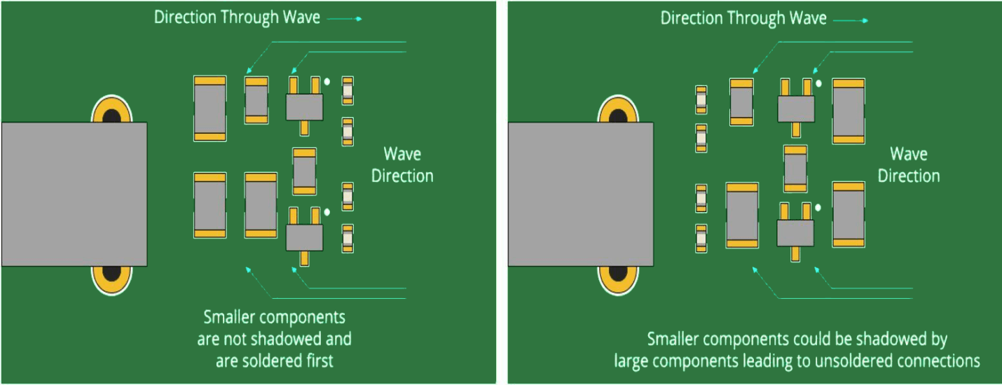
- From Layout to Manufacturable PCB
- Frequently Asked Questions (FAQs)
High speed PCB routing refers to a layout design where signal behavior follows transmission line theory. High-speed PCB layout treats traces as controlled impedance paths rather than simple conductors. Signal integrity, power integrity, and electromagnetic effects guide routing decisions in high-speed PCB design.
Traditional PCB routing focuses on electrical connectivity between components. High-speed PCB layout focuses on waveform preservation, timing accuracy, and noise control. Signal edges propagate as electromagnetic waves across traces, which creates reflections and crosstalk. Layout decisions determine impedance continuity, return path stability, and electromagnetic behavior across multilayer stackups and complex routing environments.
Defining High-Speed Constraints in PCB Design
High-speed PCB constraints get defined at the initial design stage. Signal flow mapping identifies critical nets before layout begins. Early planning establishes control over signal integrity and timing behavior.
Signal flow analysis organizes data paths and timing relationships. Critical nets include clock lines, differential pairs, and high-frequency interfaces. Constraint assignment defines impedance targets, trace length limits, and spacing rules. Routing decisions follow these constraints and reduce signal distortion.
Constraint definition embeds layout intent into the design stage. Layer stackup, reference planes, and return path continuity define the electrical structure of the board. Controlled impedance depends on dielectric thickness and trace geometry. Early constraint planning reduces redesign cycles and improves layout accuracy.
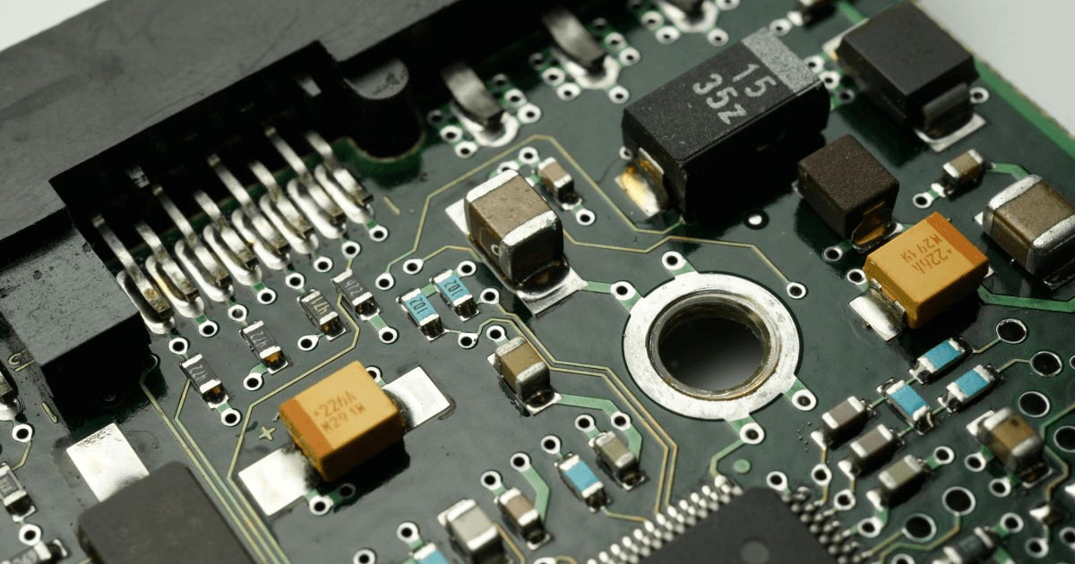
Component Placement Strategies in High Speed PCB Layout
Why Placement Directly Affects High-Speed Performance?
Component placement functions as an electrical design step in high-speed PCB layout. Placement defines signal path length, return path continuity, and impedance stability. Poor placement increases reflections, delay, crosstalk, and waveform distortion.
High-speed PCB layout requires minimal distance between drivers and receivers within critical signal paths. Shorter paths reduce propagation delay and limit signal attenuation across traces. Placement errors introduce impedance discontinuities that distort edges and degrade timing margins. Improper placement near plane splits disrupts return paths and increases loop inductance.
Component arrangement influences electromagnetic coupling across the entire board structure. Closely spaced high-speed nets increase capacitive and inductive coupling between traces. Parallel routing sections amplify crosstalk and noise transfer between signals. Spacing, orientation, and layer assignment control interference in high-speed PCB design. These parameters preserve signal integrity across dense routing regions.
Optimizing Placement for Critical Signals and Paths
Placement prioritization surrounds critical high-speed signals in PCB design. Clock sources, processors, and memory devices form tight clusters. This arrangement reduces latency and preserves timing relationships.
Differential signal components require symmetrical placement. Equal path geometry preserves signal balance and reduces noise sensitivity. Misalignment creates skew and signal degradation.
Power components require placement close to load devices. Decoupling capacitors sit near power pins to stabilize voltage. This arrangement reduces supply noise and improves high-speed PCB performance.
Power Integrity Considerations in High Speed PCB Design Guidelines
Power integrity acts as a core requirement in high-speed PCB design. Power distribution networks influence voltage stability across high-frequency circuits. Poor power integrity introduces noise that degrades signal performance.
Decoupling Strategies for High-Speed Circuits
Decoupling capacitors sit close to integrated circuit power pins. Short connections reduce parasitic inductance within the current path. Each capacitor targets specific frequency ranges within the power spectrum.
High-speed PCB layouts use multiple capacitor values for broadband decoupling. Small capacitors filter high-frequency noise near the device. Larger capacitors stabilize lower-frequency variations within the power network.
Reducing Power Noise Through Layout Optimization
Layout structure controls current flow within the power distribution network. Solid power and ground planes reduce impedance and voltage fluctuation. Continuous planes maintain stable reference conditions for high-speed signals.
Designers minimize loop area between power and ground paths. Smaller loops reduce electromagnetic radiation and switching noise. Proper placement of vias and planes improves current return efficiency and power stability.
Parasitic Effects in High Speed PCB Layout
Every high-speed PCB layout contains inherent parasitic effects. Parasitic capacitance and parasitic inductance appear within traces, pads, and vias. These unintended electrical properties arise from physical geometry and material structure.
Sources of Parasitic Capacitance and Inductance
Parasitic capacitance forms between adjacent conductors and reference planes. Trace width, spacing, and dielectric thickness influence this capacitance. Closely spaced traces increase electric field coupling between signals.
Parasitic inductance develops along current paths and via structures. Longer traces and narrow conductors increase inductive behavior. Vias introduce additional inductance due to vertical current transitions.
Impact of Parasitics on Signal Integrity
Parasitic capacitance slows signal edges and increases propagation delay. Excess capacitance distorts waveform shape and reduces timing accuracy. High-speed signals lose edge definition under capacitive loading.
Parasitic inductance causes voltage spikes and ringing within signal paths. Inductive effects increase impedance variation and reflection. Combined parasitic effects degrade signal integrity and increase electromagnetic interference.
Grounding and Return Path in High Speed PCB Layout Guidelines
Grounding acts as a reference system for high-speed PCB signals. Ground planes define return paths for signal currents. Stable return paths maintain signal integrity and reduce electromagnetic noise.
Importance of Continuous Ground Planes
Continuous ground planes create low impedance return paths beneath signal traces. High-speed PCB layout relies on uninterrupted reference planes for stable transmission. Solid planes reduce voltage fluctuation and maintain consistent impedance.
Ground continuity supports predictable current flow across the board. Signal currents follow the path of least impedance under traces. Continuous planes minimize loop area and reduce radiation.
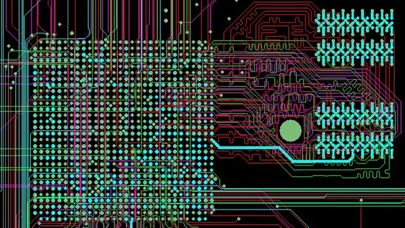
High Speed Layout Routing Techniques
Engineers apply routing discipline in high-speed PCB layout based on high-speed layout guidelines to control signal behavior. Routing decisions affect reflections, crosstalk, and electromagnetic emission. Proper trace geometry maintains waveform integrity across the board.
Trace Length Control and Loop Area Reduction
Trace length matching maintains timing alignment across related signals. Unequal lengths introduce skew and timing errors in high-speed PCB signals. Matched routing preserves synchronous data transfer between components.
Loop area reduction limits electromagnetic radiation from signal paths. Smaller loops reduce inductive coupling between adjacent nets. Tight routing around reference planes stabilizes current return paths.
Controlled Impedance and Differential Routing
Controlled impedance routing maintains consistent electrical characteristics along traces. Designers adjust trace width, spacing, and dielectric stackup for impedance targets. Stable impedance reduces reflections and signal distortion.
Differential routing uses paired traces for balanced signal transmission. Equal length and spacing maintain signal symmetry across pairs. Balanced geometry reduces noise sensitivity and improves high-speed PCB signal integrity.
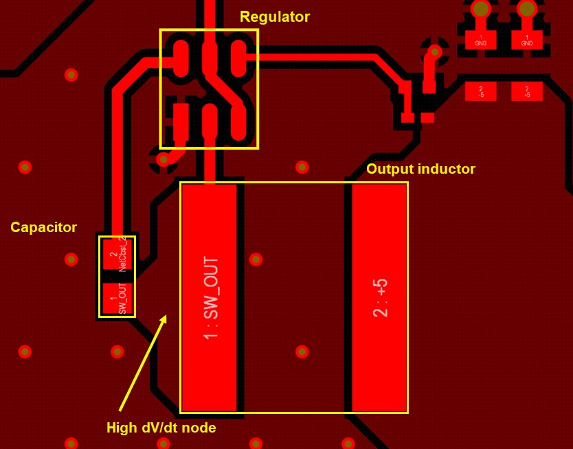
Avoiding Return Path Disruptions
Return path disruptions occur due to plane splits, gaps, or routing across voids. These interruptions force the current to detour, which increases the loop area. Larger loops increase electromagnetic interference and signal distortion.
High-speed traces avoid routing across split planes in PCB layout. Split planes interrupt return current paths and increase loop area. These interruptions degrade signal integrity and increase electromagnetic emission.
Stitching vias reconnects ground regions across separated planes. Via placement restores the return current continuity under the signal paths. Grounding strategy maintains stable current flow across high-speed PCB structures.
From Layout to Manufacturable PCB
Manufacturing rules convert high-speed PCB layout into fabrication-ready data. Design transfer defines layer stack, drill files, and impedance targets. Fabrication constraints validate final geometry and output quality.
Differences Between Conventional and High-Speed PCB Design
Conventional PCB design focuses on connectivity and component placement. High-speed PCB design focuses on signal integrity and controlled electrical behavior. Routing decisions affect timing, impedance, and electromagnetic performance.
High-speed PCB layouts require tighter tolerances for trace geometry and spacing. Fabrication processes enforce limits on copper thickness and dielectric consistency. Conventional designs tolerate wider variation in electrical parameters.
Balancing Design Rules with Real-World Constraints
Electrical requirements align with manufacturing capabilities in high-speed PCB design. Stackup selection defines impedance targets and layer distribution. Fabrication limits shape trace width and via structures.
Manufacturing review checks drill sizes, copper balance, and clearance rules. Layout adjustments match process constraints without degrading signal behavior. Final validation confirms reliable high-speed PCB production output.
High-speed PCB layout design requires careful control of constraints, power integrity, parasitics, grounding, and routing strategies. JLCPCB provides end-to-end PCB layout support that aligns signal integrity with manufacturable output.
Frequently Asked Questions (FAQs)
Q: What is the best trace width for high-speed PCB signals?
Trace width depends on target impedance and stackup geometry. Trace width depends on dielectric height and copper thickness in PCB design. Controlled impedance defines routing dimensions for stable signal behavior.
Q: How do vias affect signal integrity in high-speed PCB design?
Vias introduce inductance and disrupt signal continuity. Long via barrels increases delay and reflection risk. Via count decreases across critical nets in PCB design. Back drilling removes unused via stubs for improved signal integrity.
Q: What is the best PCB stackup for high-speed signals?
A symmetrical stackup with solid ground planes improves return path stability. Signal layers sit adjacent to reference planes in PCB design. This structure reduces impedance variation and electromagnetic interference across routing layers.
Q: How to reduce crosstalk in high-speed PCB routing?
Crosstalk forms from electromagnetic coupling between adjacent traces. Close spacing and parallel routing increase interference levels. Spacing increases between traces, and parallel routing length reduces coupling effects in PCB design.
Q: What is the best dielectric material for high-speed PCB design?
Dielectric constant affects signal velocity and impedance control. Material variation changes propagation delay across traces. Stable dielectric properties maintain consistent high-frequency performance across the PCB.
Keep Learning
RF PCB Layout: Common Design Mistakes and Practical Guidelines
Key Takeaways Impedance control is non-negotiable: Maintain consistent 50Ω impedance across all transitions, including vias, connector launches, and trace bends, to prevent reflections and signal loss. Return path integrity determines RF success: Never route RF traces over ground plane splits or slots. Provide continuous return paths with stitch vias at every layer change. Functional zoning prevents interference: Physically separate RF front-end circuitry from digital logic and power management to kee......
High Speed PCB Layout Guide for Reliable Signal Control
High speed PCB routing refers to a layout design where signal behavior follows transmission line theory. High-speed PCB layout treats traces as controlled impedance paths rather than simple conductors. Signal integrity, power integrity, and electromagnetic effects guide routing decisions in high-speed PCB design. Traditional PCB routing focuses on electrical connectivity between components. High-speed PCB layout focuses on waveform preservation, timing accuracy, and noise control. Signal edges propaga......
Signal Integrity Fundamentals in PCB Layout
In the world of PCB design, signal integrity plays a crucial role in ensuring the reliable and accurate transfer of electronic signals. Understanding the fundamentals of signal integrity is essential for electronics enthusiasts, hobbyists, engineers, students, and professionals involved in PCB design. This article will delve into the key concepts of signal integrity and explore how they influence PCB layout. By following best practices, you can optimize signal integrity and enhance the overall perform......
Microstrip v/s Stripline: Layout Difference and When to Use Them
RF (Radio Frequency) PCB design is where engineering meets art. Among the tools in an RF designer's toolkit, microstrip and stripline transmission lines are the unsung heroes. They ensure signals travel seamlessly across PCBs without succumbing to interference, loss, or impedance mismatches. But what are these lines, and how do you choose between them? Let's dive in, and to know more about PCB, see our detailed blog on PCB manufacturing. What Are Microstrip and Stripline Transmission Lines? Microstrip......
IC Board Design: A Technical Guide to PCB Layout
Why is PCB layout so important for an IC board design? PCB layout is the crucial moment when we turn the theoretical elegance of a schematic into a piece of hardware that works reliably and can be manufactured. For any complex board with a complex integrated circuit (IC), such as a microcontroller, an accelerator like an FPGA, or a sensitive RF transceiver, we are not simply connecting one point to another. PCB layout is an engineering specialty that has a huge influence on the performance, signal int......