Via Stitching in PCB Design: A Complete Guide
17 min
- Introduction
- What Is Via Stitching in PCB Design?
- Key Benefits of Via Stitching
- Via Stitching PCB Design Rules and Best Practices
- How to Add Via Stitching in EasyEDA
- Via Stitching Spacing and the Via Spacing Calculator
- Via Stitching vs Shielding
- Common Via Stitching Mistakes to Avoid
- FAQs about Via Stitching
- Conclusion: Via Stitching in PCB Design
Key Takeaways
Via stitching bonds same-net copper across layers with repeated plated vias, most often ground, to cut high-frequency impedance between regions.
A grounded via next to a signal layer transition gives return current a short local path and helps confine the field around the via.
Via fences along board edges and RF cavities suppress edge radiation, but their isolation is geometry- and frequency-dependent, with no universal dB value.
Keep stitching pitch at or below one-twentieth of the in-board wavelength as a conservative start, then tighten it for demanding RF and EMC structures.
Stitching complements solid stackup design and mechanical shielding; it replaces neither.
Introduction
A prototype comes back from the lab and everything works on the bench, yet it fails radiated emissions. Or a high-speed trace changes layer through a single via and the eye closes for no obvious reason. Or a tidy ground pour, connected at exactly one point, turns out to be a different voltage everywhere above a few hundred megahertz. These are all reference-structure problems, and via stitching is the layout technique that addresses them: rows or grids of plated vias that bond same-net copper regions across layers so high-frequency current sees one continuous piece of metal instead of several loosely joined ones.
Stitching is cheap, since it uses standard plated holes and no extra parts, but it only works when the physics cooperates. This guide covers what stitching vias actually do for grounding and return paths, where they help with EMI, how tight the spacing needs to be, and how to place them efficiently. It also draws the line where stitching stops and mechanical shielding begins.
What Is Via Stitching in PCB Design?
Via stitching is a periodic array of plated through-vias placed across same-net copper regions, usually ground pours or planes, to bond them electrically across layers. The two ideas below make the definition usable: how a stitching via differs from a signal via, and how the array ties ground planes together.
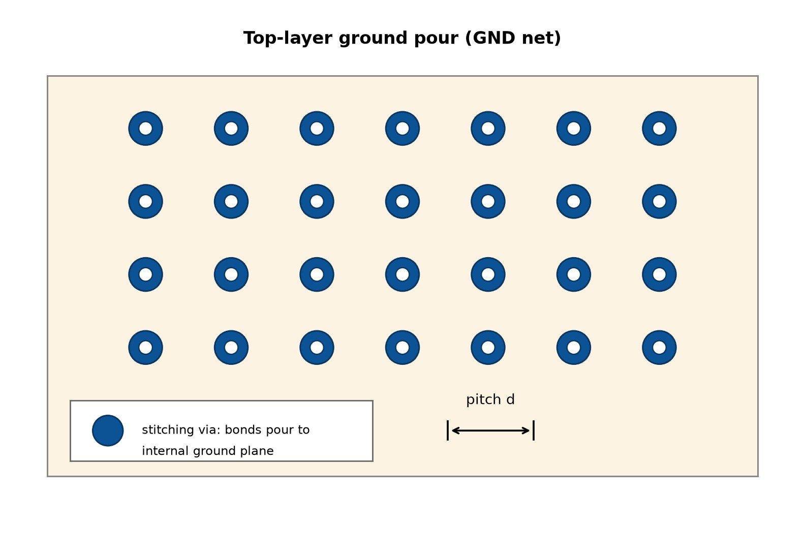
Figure 1. Stitching grid bonds the top ground pour to the internal plane at pitch d.
Stitching Vias vs. Standard Signal Vias
A signal via exists to move one routed net from one layer to another; its position is dictated by the trace. A stitching via exists to bond copper that already shares a net, and its position is chosen for electrical continuity rather than routing. Ground is the usual net because reference continuity is what most high-frequency problems come down to, though the same technique bonds power pours or other reference copper where the design calls for it.
One correction is worth making early. Stitching vias are sometimes described as carrying no current, which is only true at DC on an idle board. In a working circuit they carry return current, transient RF current, and, where pours are shared, parts of the supply current. Nor is a via barrel anything close to an ideal short: a typical 1.6 mm through-via with a 0.3 mm drill has a partial inductance on the order of 1 nH, about 1.3 nH from the standard L ≈ 5.08h[ln(4h/d) + 1] approximation. What grows into the tens of ohms at multi-GHz frequencies is its inductive reactance, XL = 2πfL, roughly 8 Ω at 1 GHz and 40 Ω at 5 GHz for that same via. Inductance in nanohenries and reactance in ohms are different quantities, and it is the reactance that makes a single stitch look increasingly lossy with frequency, which is exactly why designers use many of them in parallel.
How Via Stitching Connects Ground Planes
A multilayer board rarely has one unbroken sheet of ground. Pours get cut by via fields, slots open around connectors, and separate regions end up joined only through narrow necks or a single via. At DC that connection is fine. At high frequency its inductance dominates, so each region sits at a slightly different RF voltage and RF current takes detours around the gaps.
Repeated stitching across those boundaries puts many small inductances in parallel and pulls the regions toward the same potential. Copper left connected at only one point, or not at all, is worse: it can float up with coupled energy and re-radiate it, which is the grain of truth behind the warning that islands behave like antennas. The full picture of which layers should be adjacent in the first place is a stackup decision, covered in more depth in the guide to PCB stackup best practices.
Key Benefits of Via Stitching
Stitching earns its board space four times over, in four different physical roles. Each one below is a distinct problem with its own mechanism, from reference continuity to field confinement, and confusing them is how stitching gets misapplied.
Ground Plane Continuity and Lower Return-Path Impedance
Split or perforated ground is the most common reason stitching exists. Every gap the return current must detour around adds loop area, and loop area at high frequency means inductance, voltage drop, and radiation. A fence of stitches across the split gives the current a bridge exactly where it needs one.
The practical effect is a quieter reference: smaller voltage differences between ground regions, shorter return loops, and lower coupling into nearby traces. Mixed-signal boards feel this most, since a restless digital reference can imprint on analog grounds through shared copper. Designers sometimes hope this will cure ground bounce outright. It helps at the board level, but bounce driven inside the package or by simultaneous switching outputs has to be solved at its own source. Stitching fixes the board's share of the problem, which on a dense layout with chopped-up pours is often the dominant share.
Layer Transitions and Return Paths
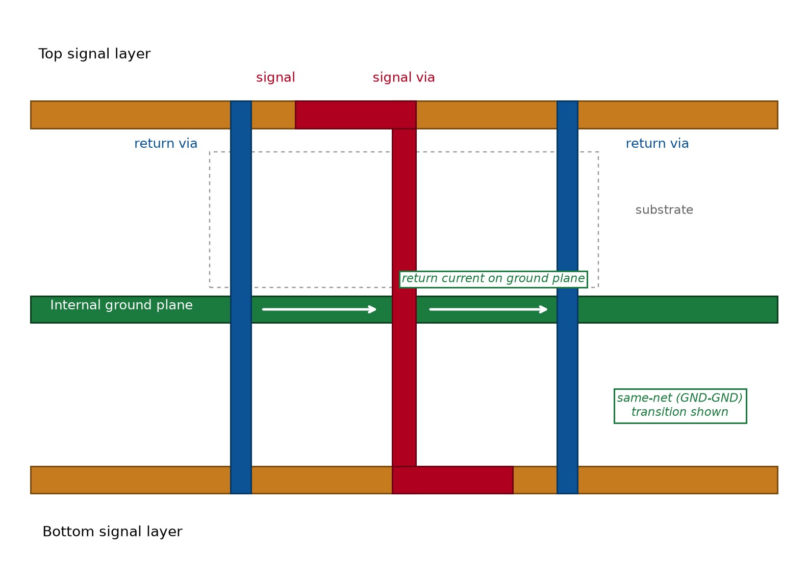
Figure 2. Case A geometry: return vias beside a same-net transition offer a short local path.
When a fast trace changes layer, the signal current dives through the via barrel while its return current must find its own way between the two reference structures. If both layers share the same continuous ground, the handoff is nearly invisible. If the references differ, or the plane is broken nearby, the return spreads out in search of a path and the discontinuity shows up as reflection and radiation.
Two cases need separating, because they ask for different copper. (A) When both layers share the same ground reference, a grounded via placed close to the transition ties the two ground structures together and hands the return current a short local path, and several of them around the signal via start to confine the field, the same idea that makes a coaxial structure quiet. (B) When the references are different nets, for example a trace moving from a ground-referenced layer to a power-referenced one, a ground via cannot bridge the two nets without shorting them. The AC return path then comes from a nearby stitching or decoupling capacitor between the planes, placed close to the transition [Texas Instruments, High-Speed Layout Guidelines].
Not every transition needs this treatment: slower digital signals with relatively slow edge rates and an unbroken shared reference may not need dedicated return vias, while fast-edge or high-speed transitions across reference discontinuities often do. Which signals qualify is a question of edge rate and reference geometry, explored in detail in the article on the impact of vias on high-speed PCB design.
EMI Reduction and Signal Integrity
A board edge where two ground layers separate behaves like a slot, and slots radiate. A line of grounded vias along the edge shorts the layers together at regular intervals so the edge can no longer support large fields between them. The same construction around an RF block forms a via fence that corrals energy where it belongs and keeps neighboring circuitry out of the field.
How much isolation a fence provides is where published numbers start to disagree. Figures quoted in the literature vary widely, and the spread is not a sign that any of them is wrong: attenuation depends on via pitch and diameter, the number of rows, the dielectric constant and board thickness, the cavity dimensions, the frequency relative to the fence resonance, and how the measurement is defined. Any single dB range quoted without those conditions attached is incomplete. The honest statement is that a tight fence relative to the wavelength isolates well and a sparse one barely isolates at all, with the details in the further reading on EMI shielding for PCBs and RF and microwave fabrication.
Thermal Management and High-Current Handling
Stitching also helps heat and current in a supporting role. Each plated barrel is a small thermal and electrical conduit between layers, so a stitched pour spreads heat wider and shares DC current across more copper than an unstitched one. That matters most around warm regulators and high-current connectors, where the extra parallel paths trim local temperature rise. Treat this as a complement to proper thermal-via arrays under hot parts and to continuous power planes, not a substitute. The full thermal treatment lives in the FR4 PCB design guidelines.
Via Stitching PCB Design Rules and Best Practices
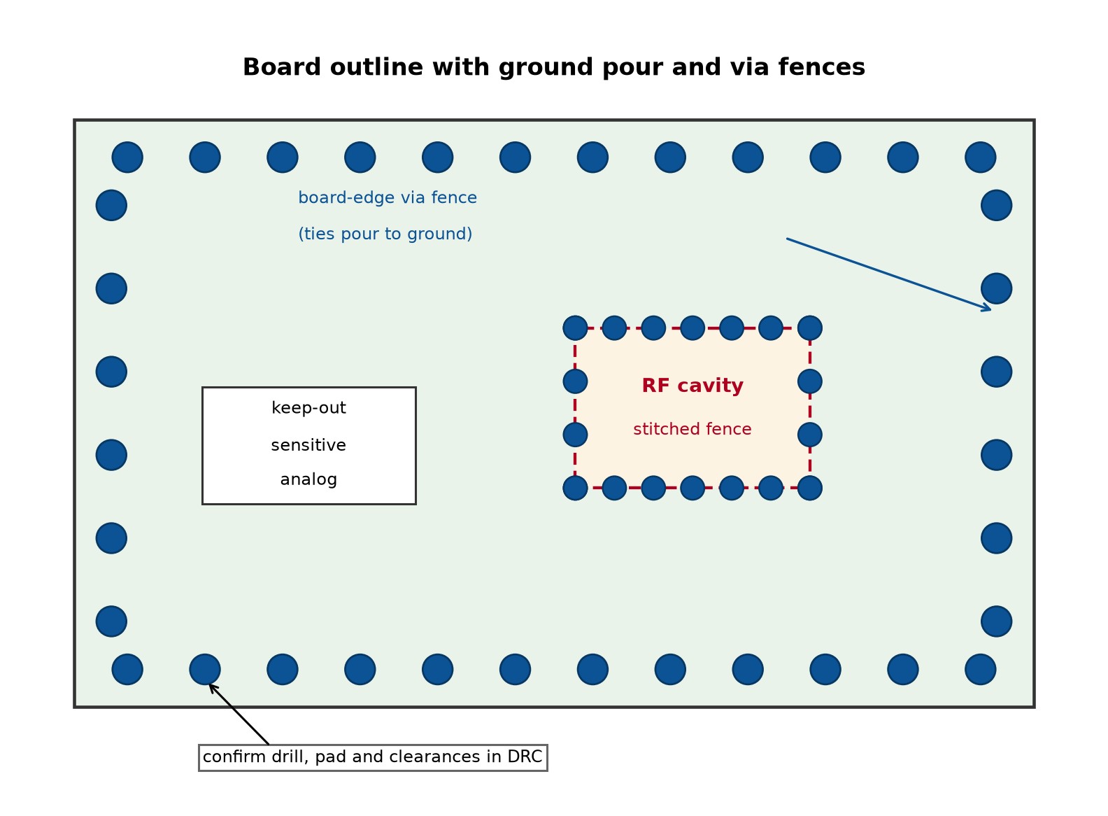
Figure 3. Edge and cavity fences, verified hole sizes, and a keep-out over analog.
Good stitching is mostly a matter of dimensions, placement, and discipline about nets. The numbers below are starting points to check against fabrication capability, not universal constants.
Size the via like any other small plated hole on the board. A 0.3 mm drill with roughly a 0.15 mm annular ring per side suits most general stitching and stays comfortably inside standard capability: the published minimum is a 0.15 mm hole with a 0.25 mm finished pad diameter, and a 0.2 mm hole is the preferred minimum for cost-sensitive work (JLCPCB, Rigid PCB Manufacturing Capabilities). Diameters far below that buy little for stitching and cost more, since only through holes are supported and tiny holes carry surcharges.
Lay general ground stitching on a loose grid that floods pours and crossings, typically on the order of a few millimeters, and tighten it deliberately where the physics demands: along board edges, across plane splits, and around RF cavities. Keep each fence as a continuous chain with no long gaps, since one missing stretch reopens the slot the rest of the fence was closing.
Nets deserve paranoia. Every stitching via must land on the intended net on every layer it touches, and the pour must actually connect to it after repouring. A via assigned to the wrong net, or stranded on an unconnected island, contributes capacitance to the wrong place and can make coupling worse.
Run design-rule checks early and respect copper-to-hole and hole-to-edge clearances rather than nudging vias closer by hand. Under and around sensitive analog sections, hold stitching back unless the return path genuinely needs it; copper texture and via antipads under a precision front end are a source of coupling, not a cure.
The PCB layout service is a convenient place to confirm via sizes and clearances against live fabrication rules before a board is committed. And one piece of perspective: at low frequencies, when stitching vias are simply bonding ground copper, their placement may be a practical convenience rather than an absolute high-frequency requirement.
How to Add Via Stitching in EasyEDA
The three mainstream layout tools all reach the same endpoint, a GND-netted array tied into the pour, by different routes. One offers a dedicated generator, the others lean on copy and array placement.
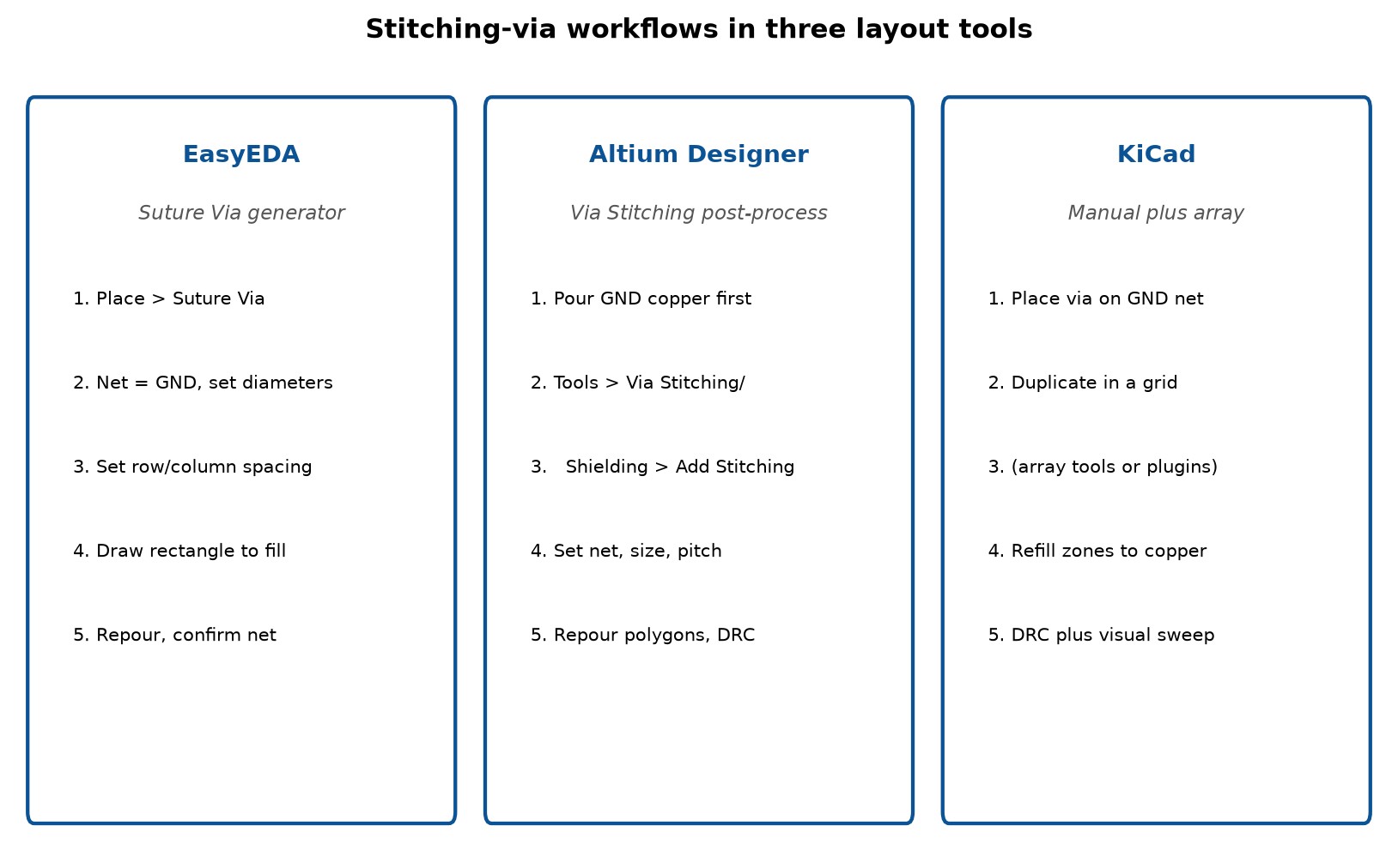
Figure 4.Verified stitching steps for each of the three layout tools covered in this section.
The via stitching EasyEDA provides comes from the suture-via function. Choose Place, then Suture Via, set the net to GND along with the outer and inner diameters and the row and column spacing, and draw the rectangle that the array should fill. The tool populates the region and steers clear of clearance violations on its own. Where a pour already exists, selecting the copper lets the array target that pour directly, so via stitching in EasyEDA stays tied to real copper instead of bare board. Repour afterward, confirm every via kept its net, and adjust the row and column spacing if the first fill lands too sparse for an edge fence.
Via Stitching Spacing and the Via Spacing Calculator
Spacing is the one stitching parameter with a formula attached, and it deserves care. The conservative rule of thumb used across RF practice is
d ≤ λ/20
where d is the center-to-center stitching pitch and the wavelength is taken at the highest significant frequency, in the board material rather than in free space. In-board wavelength follows
λ = c / (f × √εeff)
with c the speed of light, f the relevant frequency, and the effective relative permittivity of the propagation structure. Free-space wavelength overstates the spacing budget, so the dielectric belongs inside the calculation.
Highest significant frequency deserves a sentence of its own. For a clock it is not the clock rate but the spectral content of its edges; a modest-rate bus with fast drivers can carry energy far above its fundamental. Some references relax the rule to one-tenth of a wavelength. Treat one-twentieth as the cautious default for fences and RF structures, one-tenth as acceptable for ordinary ground bonding, and neither as a law of nature. Cavity dimensions, substrate height, and the actual mode structure can all demand tighter pitch, and EMC-critical geometry earns simulation or measurement rather than a rule of thumb.
A worked example pins the arithmetic down. Take a highest significant frequency of 1 GHz and assume, purely for illustration, an effective permittivity of 4.0 for the propagation structure. That value is an assumed input to the example, not a measured laminate property: bulk laminate permittivity and effective structure permittivity are different quantities, discussed below. The in-board wavelength is 3×10⁸ / (10⁹ × 2.0) ≈ 150 mm, and one-twentieth of that is 7.5 mm, about 295 mil. That is a ceiling, not a target: edge fences and RF cavities routinely go denser.
On permittivity, keep two symbols apart. Bulk relative dielectric constant describes the laminate material itself; JLCPCB documents prepreg values such as 4.4, 4.1, and 4.16 for common glass styles. Effective relative permittivity describes the actual propagation structure, including trace geometry and surrounding materials, and it is the effective value that belongs in the wavelength formula. For a real design, take it from a field solver or the stackup model behind the impedance calculator rather than from a bulk laminate table.
Note what the free impedance tool does and does not do here. JLCPCB's impedance calculator sizes trace widths and stackups for controlled impedance; it is not a stitching-spacing calculator. Set the stackup with the calculator, set the fence pitch with the wavelength rule, and refine RF geometry against the RF PCB design guidelines.
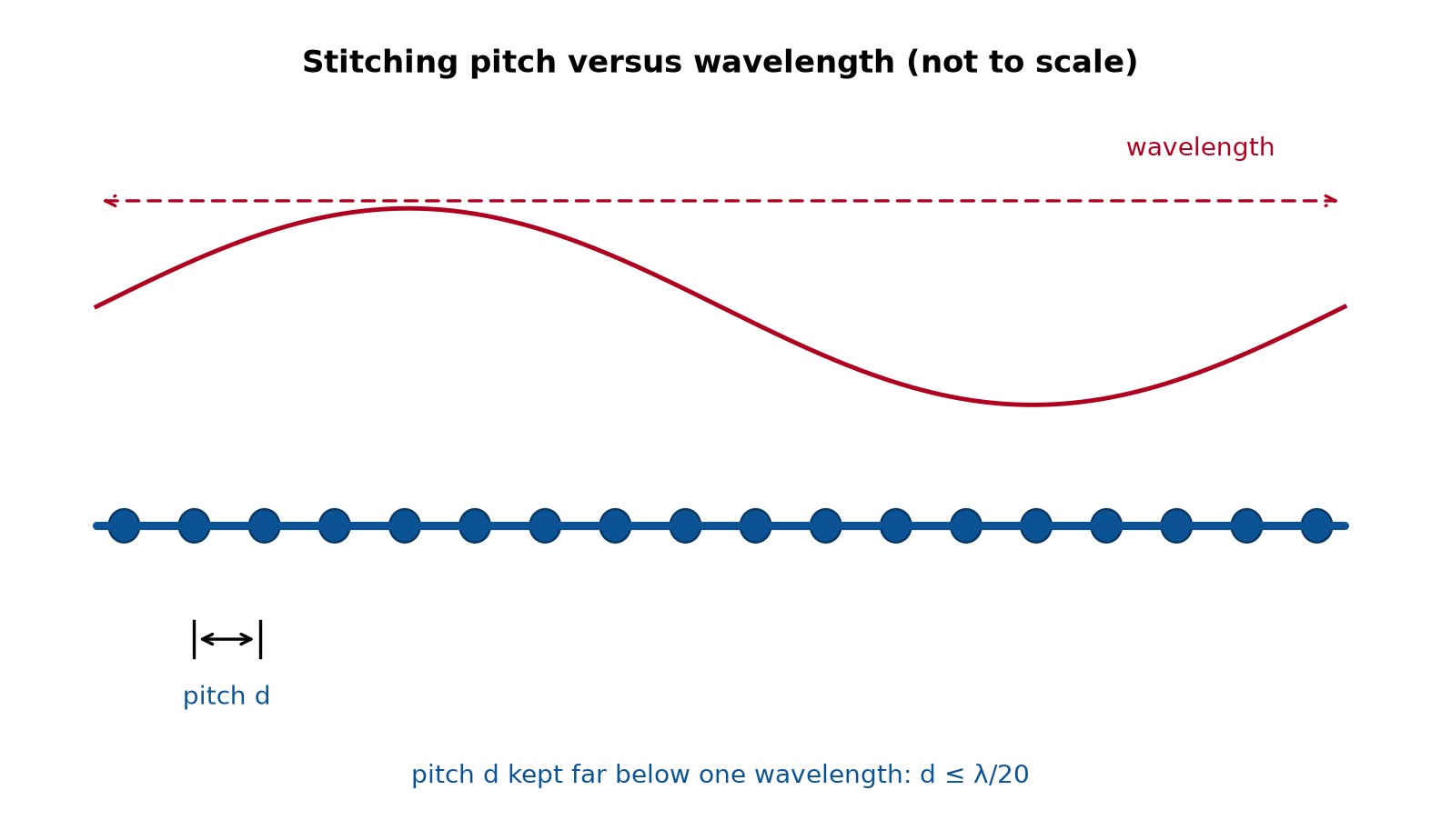
Figure 5. Pitch d is kept far below one wavelength so the array cannot behave as a resonant slot.
Via Stitching vs Shielding
Stitching and shielding answer different questions, which is why experienced layouts use both. One organizes fields inside the board; the other blocks them at the enclosure or component level. Confusion between them usually shows up as a missing shield can on a well-stitched board, or dense stitching added in hopes of fixing a system-level emissions failure that only a shield or filter can address. The table below makes the split concrete, dimension by dimension.
| Dimension | Via Stitching | Shielding |
|---|---|---|
| Working level | Board-level layout technique | Mechanical / system-level solution |
| Primary problem solved | Return paths, edge radiation, slot antennas | Radiated fields around circuits |
| Implementation | Grounded via arrays and fences | Metal shield cans over circuitry |
| Cost | Low, standard plated holes only | Higher, adds material and assembly |
| Typical use | High-speed, RF, and high-current boards | Sensitive components, RF modules, system EMC |
| Can it replace the other | No | No |
High-performance boards routinely combine them: a stitched fence around the RF section inside, a can over it. For the system-level vocabulary behind that pairing, the EMI versus EMC guide untangles which problem each technique actually solves.
Common Via Stitching Mistakes to Avoid
- Pitch chosen for the clock instead of the edges.
A fence spaced for 100 MHz leaks badly when the driver's energy peaks an order of magnitude higher, so derive spacing from the highest significant spectral content and repour the fence tighter where it matters.
- Vias with no net to call home. A stitching via that misses its pour, or a pour that never repours around the array, leaves floating copper that couples and re-radiates. Confirm net assignment and copper connection before anything else.
- A fence mistaken for a reference strategy. Stitching across a slot never repairs a trace routed over the slot; the return path under that trace stays broken. Fix the routing and the stackup first, then stitch.
- Skipped fences at edges and cavities. General grid stitching gets placed while the board edge and the RF pocket go bare, exactly where fields escape most easily. Close those chains deliberately and check DRC clearances at the outline.
FAQs about Via Stitching
Q: What is via stitching in PCB design?
It is an array of plated vias bonding same-net copper, usually ground, across layers for one low-impedance reference. Expect it wherever pours, plane splits, or board edges need bonding at high frequency.
Q: How far apart should stitching vias be?
Start from one-twentieth of the in-board wavelength at the highest significant frequency and tighten for fences and RF structures. Ordinary ground bonding often tolerates the looser one-tenth bound. Remember the dielectric sits inside the calculation, since free-space wavelength overstates the allowed pitch.
Q: Do stitching vias reduce EMI?
They can, by shortening return loops and closing radiating slots at edges and plane gaps. The improvement is structural rather than guaranteed, so emissions-critical boards still need chamber testing to confirm the result.
Q: What is the difference between via stitching and shielding?
Via stitching vs shielding is a board-versus-system split: stitching organizes return current and edge fields inside the PCB, while a shield can block radiated fields around components or assemblies. Most demanding designs use both.
Conclusion: Via Stitching in PCB Design
The thread running through every section is continuity. Wherever ground copper fragments, references part company, or an edge opens into a slot, via stitching restores one continuous structure that current can follow and fields cannot easily escape. It does that job cheaply, in standard fabrication, with no components to place.
Cheap is not the same as sufficient. Stitching complements a deliberate stackup, disciplined return-path routing, thermal design, and mechanical shielding wherever the product's emissions or susceptibility demand it, and none of those validations happen by layout alone. Draw the fences early, space them from the wavelength down rather than from habit up, and a board that passes the bench has a far better chance of passing the chamber. For dense or high-frequency layouts, professional PCB layout support is a sound backstop before fabrication.
Keep Learning
SFP Pinout Explained: PCB Layout & Design Guide
Key Takeaways The SFP pinout follows a standard 20-pin edge connector, with dedicated pins for power, ground, differential data pairs, and I2C control signals. The Tx and Rx differential pairs carry the high-speed optical or copper signal and need controlled 100 ohm differential impedance through the entire routing path. Low-speed control pins (TX_FAULT, TX_DISABLE, MOD_ABS, LOS, Rate Select/RS1) use standard single-ended routing and don't need impedance matching. Placing the SFP cage near the board e......
DDR5 PCB Layout Guidelines: Design Rules and Best Practices
Key Takeaways DDR5 raises the stakes on layout: 1.1V rails and data rates up to 8800 MT/s leave far less margin for error than DDR4 did. Target around 40–45 Ω single-ended for DQ/CA and 80 Ω differential for CLK/DQS — exact values come from vendor guidelines — and hold them through every via and connector. Keep DQ and DQS length matching within about 5 mil per byte lane, and never route a DDR5 signal over a gap in its reference plane. Plan for 8 to 12 layers with dedicated ground references next to ev......
Via Stitching in PCB Design: A Complete Guide
Key Takeaways Via stitching bonds same-net copper across layers with repeated plated vias, most often ground, to cut high-frequency impedance between regions. A grounded via next to a signal layer transition gives return current a short local path and helps confine the field around the via. Via fences along board edges and RF cavities suppress edge radiation, but their isolation is geometry- and frequency-dependent, with no universal dB value. Keep stitching pitch at or below one-twentieth of the in-b......
Crosstalk in PCB Design: Causes, Types, and How to Reduce It
Key Takeaways Crosstalk starts at an edge: a changing aggressor voltage and current produce electric and magnetic fields that couple energy into a neighboring victim trace. Edge rate matters more than clock frequency alone. A modest-rate bus with fast I/O edges can still create a serious coupling problem. More spacing and a smaller signal-to-reference-plane distance usually provide the cleanest layout improvements, but the result depends on the complete cross-section. NEXT and FEXT do not scale in the......
Mastering IC Board Design: Layout Rules & Best Practices
Key Takeaways Placement is the foundation of good layout. Position ICs, decoupling capacitors, and crystals to minimize trace lengths before routing anything — placement quality determines most of your signal performance. Respect the physics, not just the schematic. High-speed designs demand controlled impedance (e.g., 90-ohm USB differential pairs), length matching, and a well-planned layer stackup to prevent reflections, crosstalk, and power noise. Handle power and heat deliberately. Size power trac......
LVDS PCB Layout Guidelines: Design Tips and Worked Example
Key Takeaways 100 Ω Differential Impedance: LVDS PCB layout starts with one number: 100 Ω of differential impedance. Trace width, spacing, and board thickness all set that number. Route Pairs Together: Route the two traces of a pair together, side by side, and keep their lengths within 5 to 10 mil of each other. Solid Ground Plane: Never let an LVDS pair cross a gap in the ground plane. It breaks the return path and hurts the signal. 4-Layer Minimum: A 4-layer board with a solid ground plane is enough......