LVDS PCB Layout Guidelines: Design Tips and Worked Example
16 min
- Introduction
- What Is LVDS, and Why Does PCB Layout Matter?
- Key LVDS PCB Layout Guidelines
- LVDS PCB Design Example
- Common LVDS Layout Mistakes to Avoid
- FAQ about LVDS PCB Layout
- Conclusion: LVDS PCB Layout Guidelines
Key Takeaways
100 Ω Differential Impedance: LVDS PCB layout starts with one number: 100 Ω of differential impedance. Trace width, spacing, and board thickness all set that number.
Route Pairs Together: Route the two traces of a pair together, side by side, and keep their lengths within 5 to 10 mil of each other.
Solid Ground Plane: Never let an LVDS pair cross a gap in the ground plane. It breaks the return path and hurts the signal.
4-Layer Minimum: A 4-layer board with a solid ground plane is enough for most designs. Use 6 layers for bigger, busier boards.
Verify Before Routing: Check your impedance numbers before you route. Fixing this after the board is made costs much more.
Introduction
An engineer wires up an LVDS link between a processor and a screen. The board powers on. The screen flickers or shows noise.
The parts are right. The schematic is right. The problem is in the copper. This is why LVDS PCB layout guidelines matter just as much as the circuit itself.
LVDS stands for low voltage differential signaling. It sends data using two matched wires instead of one wire and a ground. This makes it fast and quiet.
You will find LVDS in screens, cameras, and car electronics. If you have ever asked what LVDS is used for, that is the short answer: anywhere fast data needs to move a short distance without making noise.
LVDS itself is easy to work with. Getting the board layout right takes more care. This article covers impedance, routing, grounding, board stackup, and termination, then walks through a real example.
None of these rules are exotic. They come down to controlling a handful of physical dimensions, trace width, trace spacing, and the distance to the nearest ground plane, closely enough that the pair behaves the way its datasheet promises. Skip one and the link may still work on the bench, then fail intermittently once the board ships in volume, sits in a hot enclosure, or picks up noise from a neighboring switching regulator.
What Is LVDS, and Why Does PCB Layout Matter?
LVDS follows a standard called TIA/EIA-644. It works a bit differently than most signals you may know.
Instead of switching one wire on and off, an LVDS chip sends a small, steady current, 3.5 mA, between two wires. At the other end, a 100 Ω resistor turns that current into a small voltage difference, about 350 mV.
The receiver only checks which wire is higher. It does not care about the exact voltage. This is why outside noise, which hits both wires the same way, gets canceled out.
This works because the two wires run side by side and carry the same signal, just inverted. A burst of noise from a nearby clock line or a switching regulator couples onto both wires by roughly the same amount at the same time. The receiver looks only at the difference between the two, so that shared noise mostly cancels before it ever reaches the logic that decodes the bit. Keeping the two traces close together and matched in length is what makes this cancellation work in practice, not just on paper.
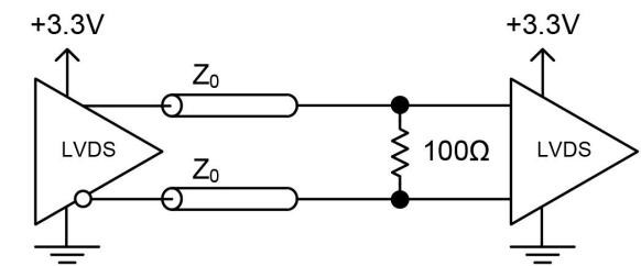
Figure1. An LVDS driver and receiver linked by a matched differential pair, with the 100 Ω termination resistor at the receiver.
This is why LVDS is naturally quiet and low noise. It is one reason engineers like it for LVDS circuit design.
But quiet by design does not mean mistake proof. A bad trace width, a length mismatch, or a noisy trace nearby can still cause errors. A small layout mistake that would not matter on a slow signal can break an LVDS link running at high speed.
So what is LVDS used for in real life? Screens, cameras, links between chips, car dashboards, and connections between two boards. All of these need a lot of data moving fast over a short, fixed distance. That fixed distance and speed is exactly why the layout has to be right the first time.
Key LVDS PCB Layout Guidelines
The next few sections cover the main rules for laying out LVDS: impedance, routing, grounding, stackup, and termination.
Get these right and you avoid signal problems, noise, and having to redo the board. A few of these rules apply to any fast signal pair, so we keep those short and link out for more detail.
Impedance Control for LVDS PCB
This is the most important rule: the pair needs to measure 100 Ω differential. This matches the resistor at the receiver.
Get it wrong, and the signal bounces back at every mismatch. That shows up as jitter, a shaky, unclear signal.
A pair that measures 90 Ω or 115 Ω instead of 100 Ω will not necessarily fail outright. But every ohm off target reflects a little more of the signal back toward the driver instead of letting it reach the receiver cleanly. Stack up a few small mismatches, a connector footprint here, a via transition there, a plane split somewhere else, and the reflections add up until the eye diagram closes and bit errors start to show up at speed.
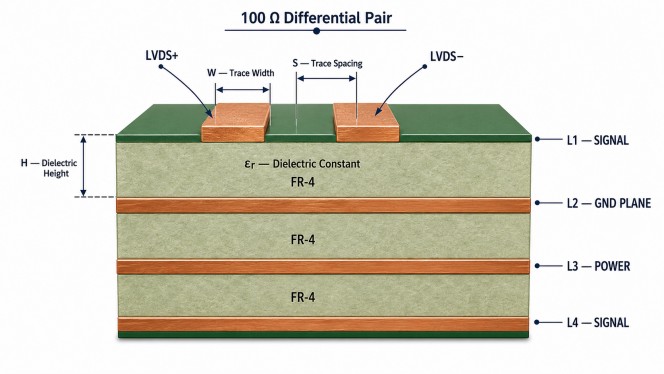
Figure2. Trace width (W), spacing (S), and dielectric height (H) are the variables that set 100 Ω differential impedance for an LVDS pair.
Trace width, spacing between the traces, and board thickness all set the LVDS impedance. Move the traces closer and impedance drops. Make the board thicker and it rises.
Because so many things affect this number, do not guess. Use the JLCPCB Impedance Calculator with your actual stackup, trace width, spacing, and dielectric thickness.
Two common LVDS routing types are microstrip (outer layer over ground) and stripline (inner layer between reference planes). Stripline traces sit buried between two ground layers. They block outside noise better, which helps in noisy parts of the board, but they are harder to probe.
Here is a simple starting point for common board types. Always confirm the exact numbers with a calculator for your own stackup.
| Board Type | Trace Width | Pair Spacing | Target Impedance |
|---|---|---|---|
| 4-layer, ~5 mil to GND | 4 to 5 mil | 6 to 8 mil | ~100 Ω |
| 6-layer, thinner core | 3.5 to 4.5 mil | 5 to 7 mil | ~100 Ω |
| Stripline (buried) | 3 to 4 mil | 5 to 6 mil | ~100 Ω |
Differential Pair Routing Best Practices
The basic rules for any differential pair, keep the two traces close, parallel, and evenly spaced, are covered in more detail in our Differential Pairs on PCBs: Best Practices article. We keep that part short here.
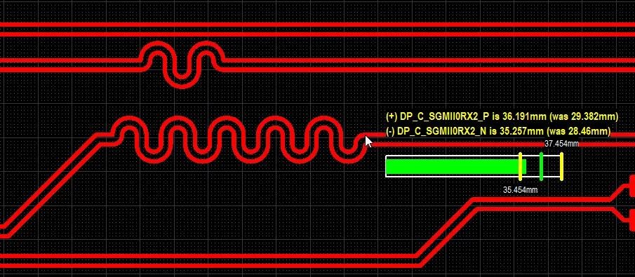
Figure3. Serpentine length tuning in a PCB layout tool: the meander on the shorter trace adds length until the two traces of the pair match within the target window.
Length matching is where people often overthink it. How close the lengths need to be depends on your speed, not on some fixed rule.
For most LVDS designs, running a few hundred Mbps up to about 1 Gbps, keeping the two traces within 5 to 10 mil of each other is plenty. You do not need to chase under 5 mil on every design.
Only add the small zigzag length tuning, called serpentine, when your actual mismatch gets close to that limit. Do not add it out of habit.
Keep vias off the pair as much as you can. Each via is a small bump in impedance, and on a fast signal that bump shows up as a weaker, noisier signal.
If a via is unavoidable, for example where a pair drops from a connector down to an inner layer, place both vias close together and add a ground via right next to them.
Keep LVDS pairs away from other fast signals, especially clocks, and keep every trace as short as you reasonably can.
Hold the spacing between the two traces constant along the entire route too. A pair that pinches together to squeeze past an obstacle, then spreads back out on the far side, creates two small impedance steps instead of a smooth 100 Ω line, and each step reflects a bit more of the signal.
Grounding and Reference Planes for LVDS
A solid, unbroken ground plane under an LVDS pair gives the return signal a clean, short path right below it.
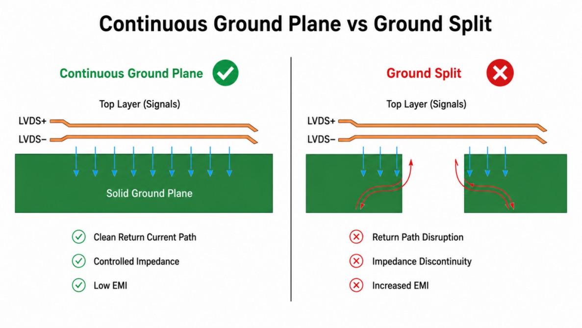
Figure4. A continuous ground plane keeps the LVDS return current directly under the signal. A split in the plane forces a detour, which disrupts impedance and raises EMI.
Why crossing a gap in that plane is bad, and how it hurts the signal, is explained fully in our other guides, so we will not repeat it all here. See the USB 3.0 Differential Signaling Design Guide for more on this.
For LVDS, route your pairs over ground, not over a power plane, whenever you can. LVDS depends on noise being equal on both wires, and a power plane tends to carry more of its own noise.
If a pair must change layers, add a small via connecting the two ground planes right next to where the signal changes layers. This keeps the return path short.
Pay extra attention right where a pair leaves a connector or crosses from one board to another. This is where ground planes are most likely to be interrupted by mounting holes, keepouts, or connector shields. A ground pin placed close to the signal pins gives the return current a short path to follow instead of forcing it to detour around the gap.
PCB Stackup Design for LVDS
A 4-layer board is the minimum for LVDS. Put signal traces on the top and bottom layers, a solid ground plane next to the LVDS layer, and power on the layer that is left.
This gives every LVDS pair a clean ground right beside it, which is what keeps impedance steady and the return path short.
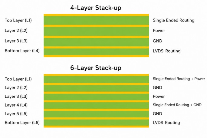
Figure5. Recommended 4-layer and 6-layer stackups, with the LVDS routing layer kept next to a solid ground plane in both configurations.
Go to 6 layers if you have a lot of LVDS pairs, a wide bus, or a board that also has noisy digital or RF sections that need their own space.
A thin gap between the signal layer and its ground plane lets you hit 100 Ω with a normal, easy to manufacture trace width. A thick gap forces skinnier traces, which are harder to make consistently.
Standard FR-4 is fine for most LVDS designs, since the data rates involved rarely push into territory where dielectric loss becomes a real problem. Save exotic, low-loss laminates for links running well above a few Gbps or for boards that also carry RF signals that need the tighter dielectric control.
LVDS Termination and AC/DC Coupling
Most LVDS links on a single board use DC coupling. That just means one 100 Ω resistor placed right across the pair at the receiver.
AC coupling adds a small capacitor on each wire. This blocks any voltage difference between the two ends, which matters when they are on separate boards, separate power supplies, or connected by a cable.
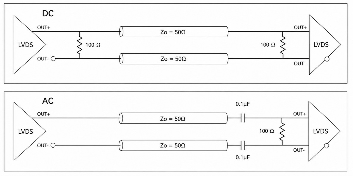
Figure6. DC-coupled LVDS termination compared with AC-coupled termination, which adds a series capacitor on each line ahead of the receiver's 100 Ω resistor.
If the driver and receiver sit on the same board and share the same ground, DC coupling is simpler and uses fewer parts. Reach for AC coupling only when you need to break a ground loop, connect boards that do not share a supply, or run the link through a cable where the two ends may sit at slightly different potentials.
Here is a quick side-by-side comparison of the two:
| DC Coupling | AC Coupling | |
|---|---|---|
| Extra parts | None, just the 100 Ω resistor | Series capacitor on each trace |
| Best for | Same board, same ground | Different boards or power domains |
| Blocks DC offset | No | Yes |
| Common use | On-board display links | Cable or connector links |
Many newer LVDS chips already have the resistor built in. Check the datasheet first. Adding your own resistor on top of a built-in one will throw off your impedance.
LVDS PCB Design Example
This LVDS PCB example walks through a real display interface design, showing how the guidelines come together in practice. The goal is to route an LVDS link from a processor to a board-to-board connector that feeds an LCD panel. The interface uses four data pairs and one clock pair, running at a typical display data rate.
The first step was choosing a 4-layer stackup. This gave a solid ground plane directly beneath the top signal layer, which is where all LVDS traces would live. A 4-layer board is enough for most display links, and keeping the LVDS layer next to ground made impedance control straightforward.
All five differential pairs were routed on the top layer with constant spacing. Each pair was kept close together, with the two traces within 8 mil of each other in length. No serpentine tuning was needed because the route was short and the mismatch stayed within budget. Vias were avoided entirely; the pairs ran straight from the processor to the connector without dropping to another layer.
The LCD panel's receiver had its 100 Ω termination built in, so no external resistors were needed on this board. This is worth confirming early in the design: if the receiver does not include internal termination, the external 100 Ω resistor belongs across the pair right at that receiver's input pins — not at the driver-side connector. A resistor placed mid-link, on the connector of the driver board, does not terminate the line; it only creates a stub and adds a second load for the driver to drive.
The ground plane beneath the LVDS traces was left completely solid. No cuts, no slots, no copper pours that interrupted the return path. The connector had ground pins placed next to every LVDS signal pin, giving the return current a clean path from the processor to the panel.
The total route length was kept under 50 mm. This is short enough that insertion loss was not a concern, and the signal arrived at the receiver with plenty of margin. The pairs were spaced evenly, with extra clearance from any nearby clock lines or power traces.
With these choices in place, the link passed timing and signal-integrity checks on the first board spin. No rework was needed on the differential pairs, which is the whole point of checking impedance and planning the stackup before routing starts instead of after the board comes back from fabrication.
Common LVDS Layout Mistakes to Avoid
Mistakes to Avoid
- Routing over a gap in the ground plane. This forces the return signal to go around the gap, which adds noise. Keep solid ground under the whole length of every pair.
- Skipping length matching. Leaving the two traces at different lengths adds timing error, which weakens the signal at higher speeds. Match lengths based on your actual speed.
- Using too many vias. Each via adds a small bump in impedance, and an unused via stub can act like a tiny antenna at high enough speeds. Keep pairs on one layer when you can, and if you must change layers, keep the two vias close together.
- Routing LVDS near power traces. A switching regulator next to an LVDS pair can dump noise straight into it, especially at the regulator's switching frequency and its harmonics. Keep LVDS away from power circuits, and add extra spacing around any inductor or high-current node.
- Ignoring impedance. Guessing at trace width instead of checking it leads to a weaker, bouncier signal. Always check your numbers before routing.
- Adding termination twice. Adding your own resistor on top of one already built into the chip throws off the impedance. Check the datasheet first.
FAQ about LVDS PCB Layout
Q: What impedance should an LVDS pair be?
100 Ω differential. This matches the resistor normally used at the receiver.
Q: How closely do the two traces need to match in length?
It depends on your speed. For most LVDS links up to about 1 Gbps, keeping them within 5 to 10 mil of each other is enough.
Q: Can I route an LVDS pair across two layers?
Try to keep each pair on one layer. If you must change layers, use two vias placed close together, with a ground via next to them.
Q: Is 4 layers enough for LVDS?
Yes, for most designs. A 4-layer board with solid ground next to the signal layer works well. Go to 6 layers for bigger or busier boards.
Q: Do I need to add my own termination resistor?
Not always. Many LVDS chips already have one built in. Check the datasheet before adding your own.
Q: LVDS is already quiet, so why does impedance still matter?
Because being quiet by design does not protect a link from layout mistakes. A bad trace width, a gap in the ground plane, or a length mismatch can still cause problems.
Q: How do I check impedance after the board is fabricated?
A time-domain reflectometer (TDR) is the standard tool. It sends a fast edge down the trace and reads back reflections, showing the actual impedance along the length of the pair rather than just a calculated estimate.
Q: Does LVDS need special PCB material like Rogers, or is standard FR-4 fine?
Standard FR-4 works for most LVDS designs. Reserve low-loss laminates for links running well above a few Gbps or boards that also carry RF signals needing tighter dielectric control.
Conclusion: LVDS PCB Layout Guidelines
Good LVDS PCB layout comes down to a few simple habits: hit 100 Ω, keep the traces matched and close together, keep solid ground underneath, pick the right stackup, and terminate it correctly, just once. None of this is hard on its own. Problems happen when one of these steps gets skipped under a deadline. Follow these steps from the start, and your board has a much better chance of passing testing the first time, with less noise and fewer surprises.
If you are working on an LVDS board and want a second set of eyes before you send it off, JLCPCB's PCB layout services can check your stackup, routing, and impedance while it is still easy to fix.
Keep Learning
SFP Pinout Explained: PCB Layout & Design Guide
Key Takeaways The SFP pinout follows a standard 20-pin edge connector, with dedicated pins for power, ground, differential data pairs, and I2C control signals. The Tx and Rx differential pairs carry the high-speed optical or copper signal and need controlled 100 ohm differential impedance through the entire routing path. Low-speed control pins (TX_FAULT, TX_DISABLE, MOD_ABS, LOS, Rate Select/RS1) use standard single-ended routing and don't need impedance matching. Placing the SFP cage near the board e......
DDR5 PCB Layout Guidelines: Design Rules and Best Practices
Key Takeaways DDR5 raises the stakes on layout: 1.1V rails and data rates up to 8800 MT/s leave far less margin for error than DDR4 did. Target around 40–45 Ω single-ended for DQ/CA and 80 Ω differential for CLK/DQS — exact values come from vendor guidelines — and hold them through every via and connector. Keep DQ and DQS length matching within about 5 mil per byte lane, and never route a DDR5 signal over a gap in its reference plane. Plan for 8 to 12 layers with dedicated ground references next to ev......
Via Stitching in PCB Design: A Complete Guide
Key Takeaways Via stitching bonds same-net copper across layers with repeated plated vias, most often ground, to cut high-frequency impedance between regions. A grounded via next to a signal layer transition gives return current a short local path and helps confine the field around the via. Via fences along board edges and RF cavities suppress edge radiation, but their isolation is geometry- and frequency-dependent, with no universal dB value. Keep stitching pitch at or below one-twentieth of the in-b......
Crosstalk in PCB Design: Causes, Types, and How to Reduce It
Key Takeaways Crosstalk starts at an edge: a changing aggressor voltage and current produce electric and magnetic fields that couple energy into a neighboring victim trace. Edge rate matters more than clock frequency alone. A modest-rate bus with fast I/O edges can still create a serious coupling problem. More spacing and a smaller signal-to-reference-plane distance usually provide the cleanest layout improvements, but the result depends on the complete cross-section. NEXT and FEXT do not scale in the......
Mastering IC Board Design: Layout Rules & Best Practices
Key Takeaways Placement is the foundation of good layout. Position ICs, decoupling capacitors, and crystals to minimize trace lengths before routing anything — placement quality determines most of your signal performance. Respect the physics, not just the schematic. High-speed designs demand controlled impedance (e.g., 90-ohm USB differential pairs), length matching, and a well-planned layer stackup to prevent reflections, crosstalk, and power noise. Handle power and heat deliberately. Size power trac......
LVDS PCB Layout Guidelines: Design Tips and Worked Example
Key Takeaways 100 Ω Differential Impedance: LVDS PCB layout starts with one number: 100 Ω of differential impedance. Trace width, spacing, and board thickness all set that number. Route Pairs Together: Route the two traces of a pair together, side by side, and keep their lengths within 5 to 10 mil of each other. Solid Ground Plane: Never let an LVDS pair cross a gap in the ground plane. It breaks the return path and hurts the signal. 4-Layer Minimum: A 4-layer board with a solid ground plane is enough......