Crosstalk in PCB Design: Causes, Types, and How to Reduce It
16 min
- Introduction
- What Is Crosstalk in PCB Design?
- What Causes Crosstalk in PCB Designs?
- Types of Crosstalk
- Crosstalk in PCB Design Example
- How to Reduce Crosstalk in PCB Designs
- FAQ about Crosstalk in PCB Design
Key Takeaways
Crosstalk starts at an edge: a changing aggressor voltage and current produce electric and magnetic fields that couple energy into a neighboring victim trace.
Edge rate matters more than clock frequency alone. A modest-rate bus with fast I/O edges can still create a serious coupling problem.
More spacing and a smaller signal-to-reference-plane distance usually provide the cleanest layout improvements, but the result depends on the complete cross-section.
NEXT and FEXT do not scale in the same way. NEXT reaches a geometry-dependent plateau after a sufficient coupled delay; FEXT depends on modal-velocity mismatch as well as coupled length.
Treat 3W, 5W, 3H, and wavelength-based via spacing as starting heuristics. Verify critical nets with a field solver, coupled transmission-line model, or measurement.
Introduction
A memory interface can pass a short bench test and still fail intermittently at full traffic, temperature, or voltage corners. The logic is correct, yet one data line receives enough noise from its neighbors to erode the receiver margin. That is a typical crosstalk in PCB design problem: the board geometry has become part of the circuit.
Crosstalk is common on dense digital boards because adjacent conductors share electric and magnetic fields. Faster I/O edges increase the coupled transient even when the clock or data repetition rate appears modest. Trace spacing, parallel length, driver impedance, termination, reference planes, and stackup all change what reaches the victim. This article follows the physical path from an aggressor transition to the resulting noise, then separates near-end crosstalk (NEXT) from far-end crosstalk (FEXT). It closes with an illustrative DDR case and practical ways to reduce coupling without turning layout rules of thumb into guarantees.
What Is Crosstalk in PCB Design?
Crosstalk is unwanted energy transferred from one PCB interconnect, the aggressor, to another interconnect, the victim, through electromagnetic coupling. The traces do not need a conductive connection; mutual capacitance and mutual inductance are enough to produce a noise waveform on the victim.SCAA082A
The effect occurs while voltage or current is changing. A digital transition launches fields around the aggressor. Some electric-field flux terminates on the victim instead of the reference plane, while some magnetic flux links the victim's current loop. Those interactions inject current and induce voltage on the victim. The resulting disturbance then propagates along the victim transmission line and can reflect if its terminations are mismatched.
This is why a crosstalk signal integrity review starts with edge rate rather than clock frequency alone. A 25 MHz control signal with a 500 ps edge can couple strongly through an unfortunate geometry. Transition time, voltage swing, output impedance, and return path all matter. Good PCB trace design therefore treats fast nets as transmission structures, not ideal schematic wires.
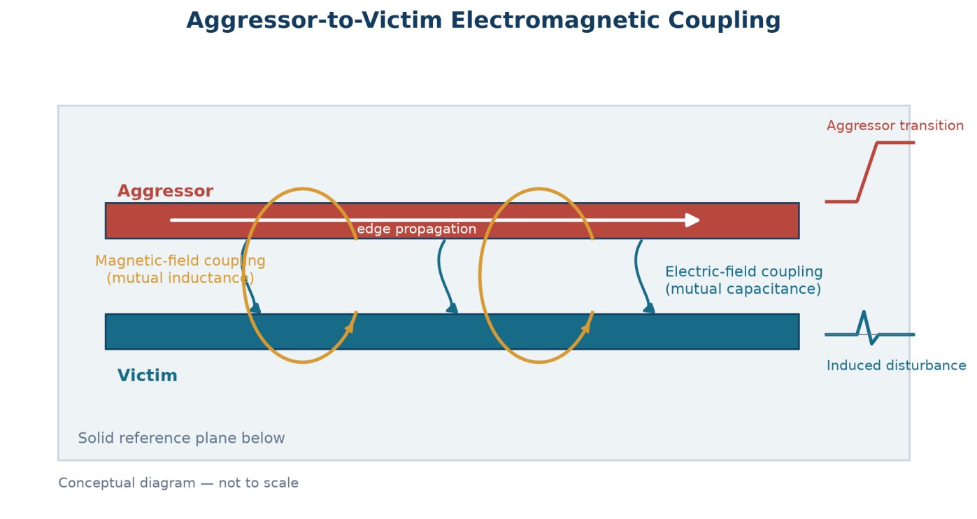
Figure 1. Electric- and magnetic-field coupling between aggressor and victim PCB traces (conceptual, not to scale).
What Causes Crosstalk in PCB Designs?
Crosstalk is set by identifiable electrical and geometric conditions. Close spacing increases mutual coupling; a long shared route gives the fields more distance over which to interact; fast edges raise voltage and current slew rates; and a distant or discontinuous reference plane lets the fields spread. Driver and victim impedances, terminations, layer geometry, dielectric properties, and nearby copper determine the waveform that finally appears at the receiver.
Capacitive and Inductive Coupling
Adjacent traces have distributed mutual capacitance. For a differential segment of coupled length, the local mutual capacitance follows:
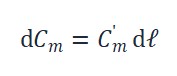
The primed quantity is mutual capacitance per unit length. When the aggressor voltage changes, that element drives displacement current toward the victim:
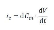
A larger per-unit-length coupling, longer interacting region, larger voltage swing, or shorter transition time changes the resulting coupled waveform. The victim impedance and its terminations convert the distributed current into a voltage disturbance.
The aggressor current also creates a magnetic field. For the same differential segment, the local mutual inductance follows:
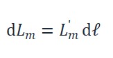
The primed quantity is mutual inductance per unit length. A changing aggressor current induces a local series voltage:
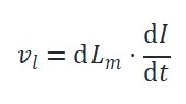
Both mechanisms act at the same time. The per-unit-length mutual capacitance and inductance are distributed along the coupled region. This crosstalk coupling depends on trace dimensions, spacing, plane distance, dielectric environment, and surrounding conductors. In a coupled-line model, both mechanisms launch waves toward each victim end; NEXT and FEXT cannot be assigned exclusively to capacitance or inductance.Application Note 337 Reducing Noise on Microcomputer Buses
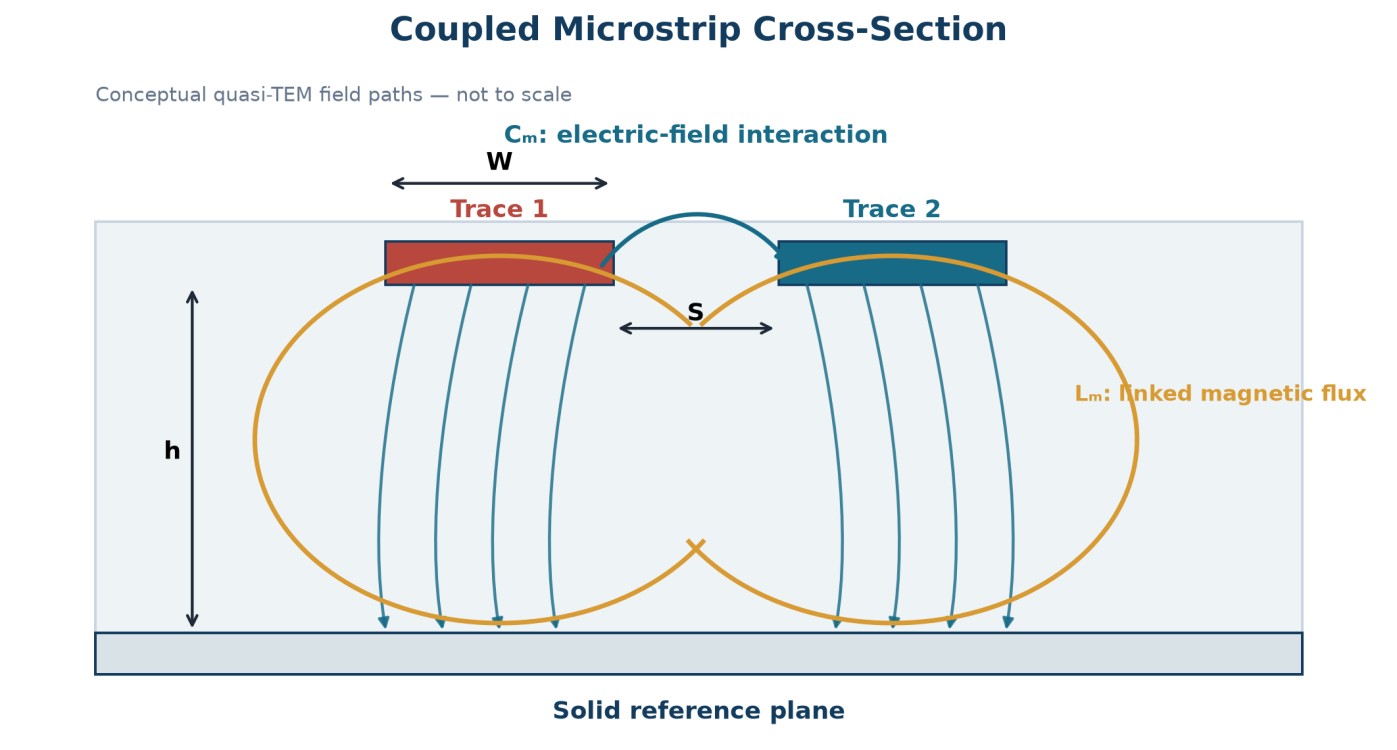
Figure 2. Mutual capacitance and mutual inductance in a coupled microstrip cross-section (conceptual, not to scale).
Factors That Increase Crosstalk Severity
Spacing is usually the first lever. As the traces move apart, less electric flux terminates on the neighboring conductor and less magnetic flux links its loop. The reduction is not governed by one universal inverse-square law. It depends on ratios such as spacing to trace width and spacing to plane height, plus the dielectric and copper geometry.
Coupled length matters, but not as a single linear rule for every observed peak. A longer uniform region changes the duration, timing, and superposition of coupled waves. FEXT commonly grows with length in the weak-coupling, short-edge approximation. NEXT rises only until contributions no longer pile up within the aggressor edge; its plateau is then set mainly by cross-section and termination.
Fast transitions raise voltage and current slew rates. Changing a clock divider does not slow the physical edge produced by the I/O buffer, so reducing repetition frequency alone may leave the crosstalk pulse nearly unchanged. Traces far from their reference plane also tend to couple more strongly because the fields spread farther laterally. Plane splits, voids, and poorly managed layer transitions enlarge or disrupt return paths and can add common-impedance coupling to the trace-to-trace mechanism. TI recommends routing high-speed signals over solid reference planes and avoiding plane splits or voids beneath them.Spraar7j
Types of Crosstalk
NEXT and FEXT describe where the coupled waveform is observed. The PCB transmission-line model explains why the electric and magnetic contributions combine differently at the two victim ends and why microstrip and stripline do not behave identically.
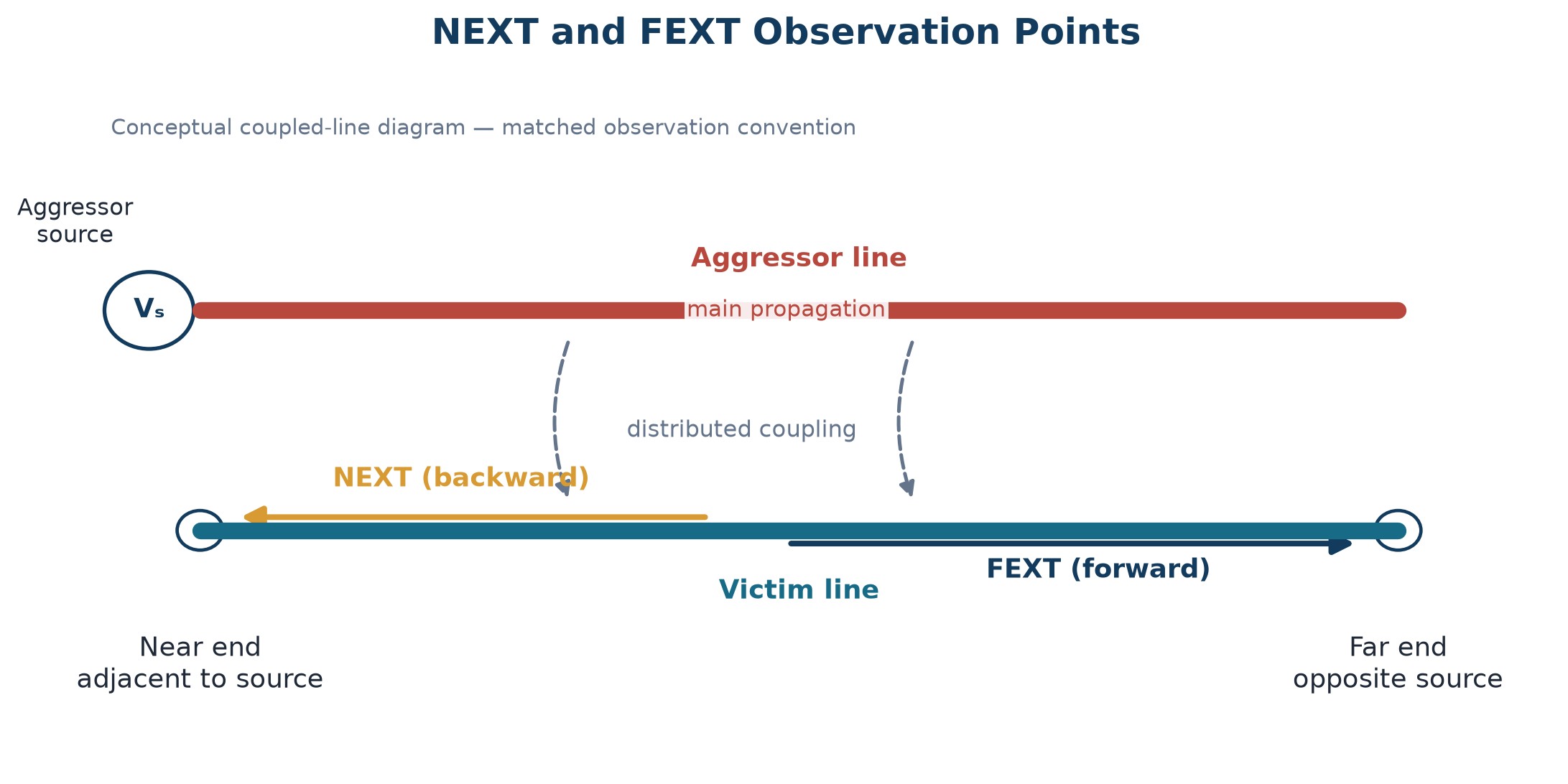
Figure 3. Near-end and far-end crosstalk observation points on coupled transmission lines (conceptual).
Near-End Crosstalk (NEXT)
NEXT is the victim noise measured at the end adjacent to the aggressor source. Each small section launches a backward-going contribution. Let the symbols below denote the one-way propagation delay through the coupled region and the aggressor rise time. For a matched, uniform, weakly coupled line, the far end stops adding to the NEXT plateau when the round-trip separation approaches the edge duration:
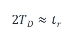
The one-way delay equals the coupled length divided by the propagation velocity:
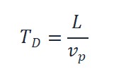
Substitution gives the corresponding approximate saturation length:
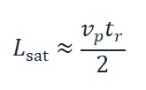
The approximation is sensitive to how rise time is defined, so use one convention, such as 10-90%, consistently. Beyond this length, more coupling mainly extends the NEXT pulse rather than raising its matched-line plateau.
Below that length, changing the coupled length can alter the peak as well as the pulse width. Reflections and unmatched terminations can then reshape or multiply the observed disturbance, so "saturated NEXT" is a matched, uniform-line concept rather than a universal ceiling for a real routed net.
Far-End Crosstalk (FEXT)
FEXT is measured at the victim end opposite the aggressor source. At that end, the electric- and magnetic-coupling contributions have opposite polarity. Their cancellation depends on the relationship between the even- and odd-mode propagation velocities.
A symmetric stripline embedded in a nearly homogeneous dielectric can make those velocities very similar, so ideal FEXT cancellation is strong. It is still inaccurate to say that stripline has no FEXT. Core/prepreg differences, offset geometry, nearby copper, glass weave, vias, bends, terminations, and loss prevent ideal symmetry. Microstrip is inherently inhomogeneous because its fields occupy dielectric and air or solder mask, so its modal velocities differ more and its FEXT is often larger.
For a uniform, weakly coupled line, FEXT generally increases with coupled length and with faster edges. In a real channel, dispersion, reflections, multiple aggressors, and the exact victim loading can change the peak and polarity. Use geometry-specific simulation rather than assigning stripline a blanket exemption.
Crosstalk in PCB Design Example
Consider eight DQ traces from an illustrative DDR byte lane, not measured test data. DQS and DM/DBI are omitted for clarity; no DDR generation, data rate, I/O model, or measured root cause is implied. Each DQ is about 4 mil wide, with roughly 4 mil edge-to-edge spacing over several inches. Errors appear during full-rate traffic and cluster on lines with active neighbors.
A first review should not declare "excessive FEXT" from symptoms alone. Check the receiver margin, power integrity, timing, reflections, reference continuity, package coupling, and simultaneous-switching behavior. Then simulate the routed byte lane with the controller and memory IBIS models, the actual stackup, terminations, and realistic switching patterns. A quiet victim between two in-phase aggressors is a useful screening case; protocol-valid activity is needed for final margin analysis.
In this scenario, the nearest neighbors have the strongest coupling because they share the smallest spacing and longest continuous parallel region. The layout team might increase the gap to about 8 mil where escape geometry permits, break up continuous adjacency, and move the bus to a layer with a thinner dielectric to its solid reference plane. If inner-layer routing provides a more homogeneous field distribution without creating bad via transitions, it may reduce FEXT but not necessarily NEXT. Total coupling still depends on spacing, dimensions, plane distances, and terminations. Recalculate trace width to preserve impedance when the dielectric height changes.
Figure 4 reports an original first-order simulation rather than measured DDR data. A two-dimensional quasi-static finite-difference solution extracted the per-unit-length capacitance matrix for each coupled-microstrip cross-section; a companion air-filled solution supplied the external inductance matrix, and a lossless multiconductor transmission-line modal model calculated the far-end victim response.Analysis of Multiconductor Transmission Lines Both cases use a 1.2 V pulse, 250 ps 10-90% source rise time, 3 in coupled length, relative permittivity 4.0, 40 ohm source resistance, and 50 ohm load per conductor. The baseline geometry (4 mil width, 4 mil gap, 3 mil plane height) produced 33.5 mV peak absolute FEXT. The revised geometry (3 mil width, 8 mil gap, 2 mil plane height) produced 12.0 mV. These are simulated values, not measurements. The lossless pair model omits packages, vias, conductor and dielectric loss, solder mask, glass weave, and receiver nonlinearity, so product sign-off still requires the routed topology and actual I/O models.
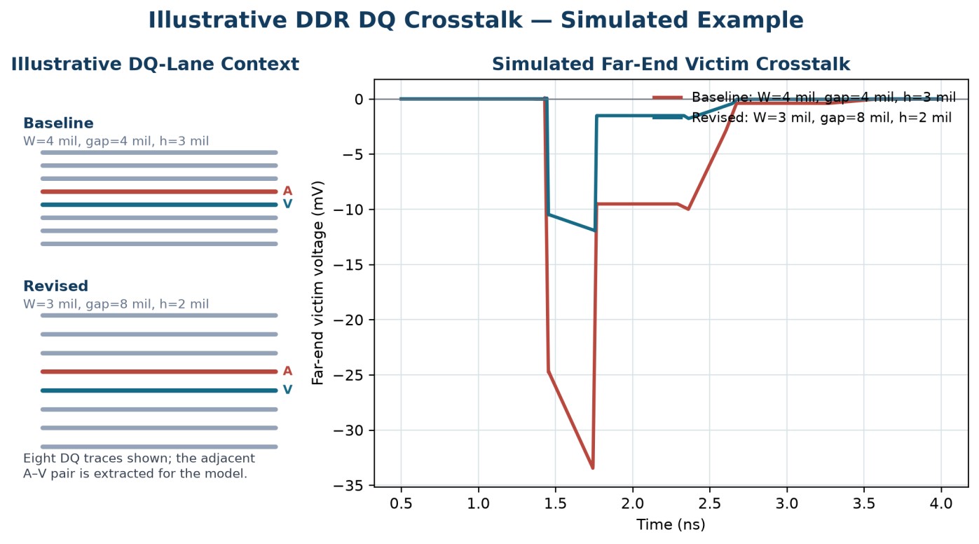
Figure 4. Simulated far-end victim crosstalk for baseline and revised illustrative DDR DQ geometry.
The quasi-TEM pair model uses a 1.2 V pulse, 250 ps 10-90% rise time, 3 in coupled length, relative permittivity 4.0, 40 ohm source resistance, and 50 ohm load per conductor. Simulated, not measured.
How to Reduce Crosstalk in PCB Designs
The best time to control coupling is while the stackup and routing rules are still flexible. A broader signal-integrity fundamentals review can cover return paths and impedance in more depth; the methods below focus on the physical levers behind crosstalk.
Increase Trace Spacing (3W and 5W Rules)
Increasing separation reduces both mutual capacitance and mutual inductance. The 3W rule, usually stated as center-to-center spacing of three trace widths, and the more conservative 5W rule are routing heuristics, not performance specifications. They do not guarantee a 70% reduction or any fixed noise level. Plane height, coupled length, edge rate, and loading still matter. Use trace-spacing guidance as a starting constraint, then simulate nets whose noise margin is tight.
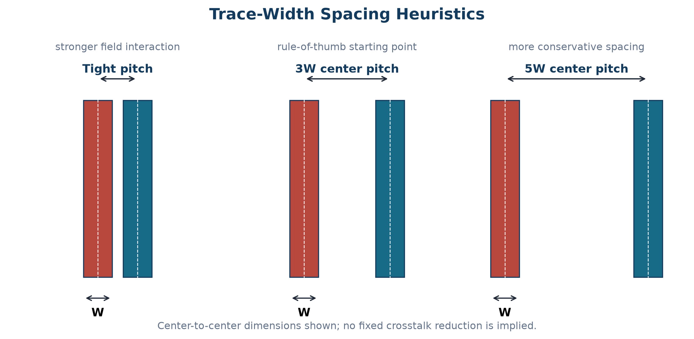
Figure 5. The 3W and 5W routing heuristics use center-to-center distance; neither guarantees a fixed crosstalk reduction (conceptual).
Minimize Parallel Run Length
Shorter side-by-side regions usually reduce the total interaction and are especially useful for limiting FEXT in uniform coupled runs. Reroute so the same two nets do not remain nearest neighbors for the entire bus, and avoid dense serpentine segments beside unrelated signals. On adjacent signal layers, use a reference plane between layers where possible rather than relying only on orthogonal routing.
Do not expect every peak to fall in direct proportion to length. Shortening the region can move coupled pulses in time or change how they overlap, while saturated NEXT may retain a similar plateau. Compare the complete time-domain waveform at the receiver.
Optimize the Layer Stackup and Reference Planes
Bring critical traces closer to a solid reference plane. A smaller signal-to-plane distance confines more of the electric field between signal and plane, reduces lateral field spread, and shrinks the signal-return loop. Recalculate trace width to maintain impedance; changing the plane distance without recalculating width may move the line away from its target impedance.
Stripline often gives better FEXT cancellation because its dielectric environment can be more homogeneous, but the actual cross-section controls the result. Define dielectric height as the distance to the nearest reference plane and trace gap as edge-to-edge clearance. Starting with a gap of at least three times the dielectric height, or wider for sensitive nets, may transfer better than a width-only rule. Values from three to five times that height remain heuristics. Consult PCB design guidelines, fabricator material data, and a field solver.
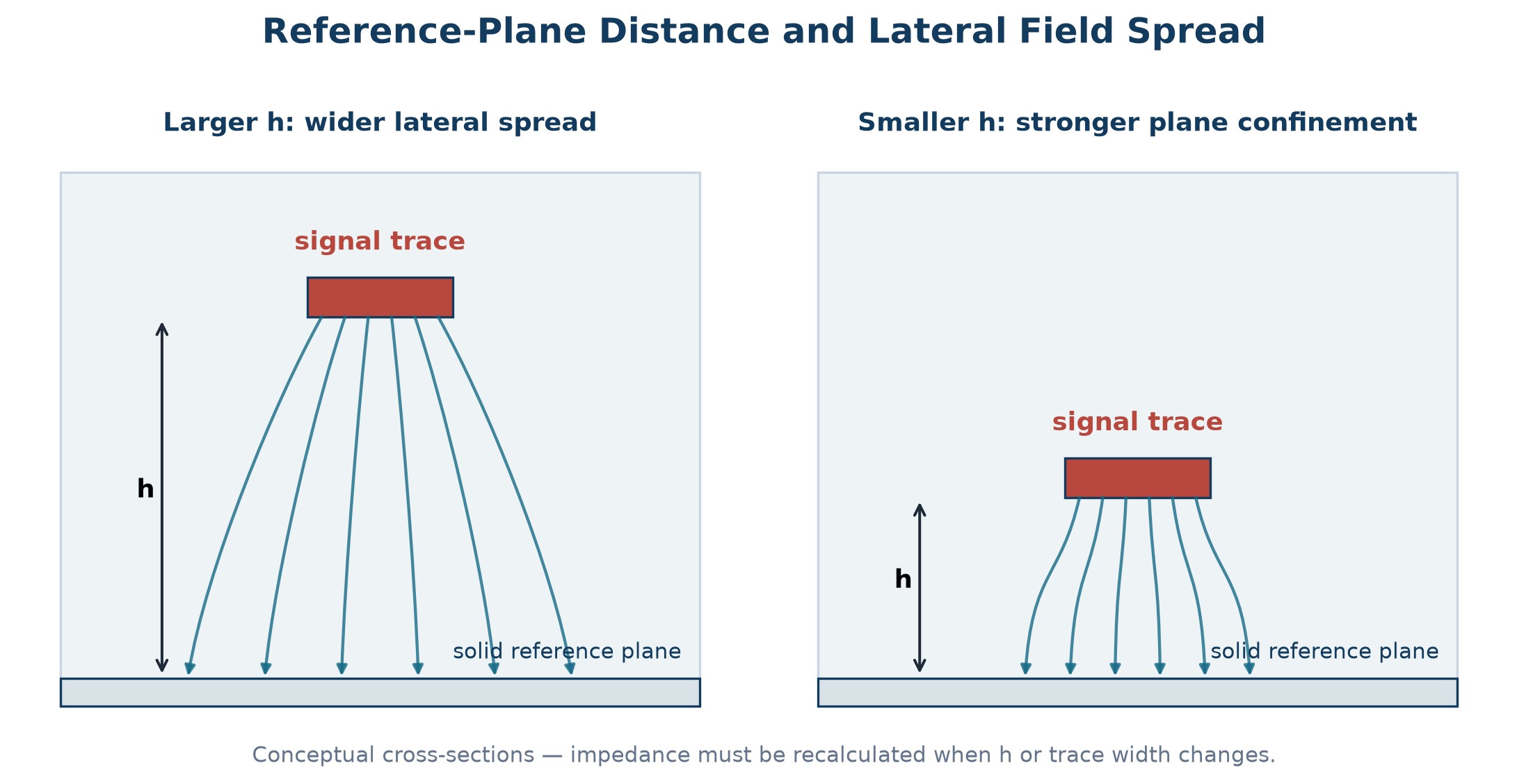
Figure 6. Reducing signal-to-plane distance confines more of the field near the reference plane and reduces lateral field spread (conceptual, not to scale).
Use Guard Traces and Ground Via Stitching
A guard trace consumes spacing, and spacing alone may provide most of the improvement. If the guard is left floating or poorly referenced, it becomes another coupled conductor and can increase crosstalk. Bogatin and Simonovich therefore recommend treating guard traces as a last resort.
When a guard is justified, tie it repeatedly to the same reference conductor used by the adjacent signals and model the complete structure. If that reference is a power plane, include its AC path and spreading inductance. A pitch of one twentieth of the selected wavelength is only a starting estimate: wavelength depends on propagation velocity and the chosen upper frequency, while vias, antipads, and cavity modes also matter. Connections only at the ends do not guarantee a quiet guard between them.
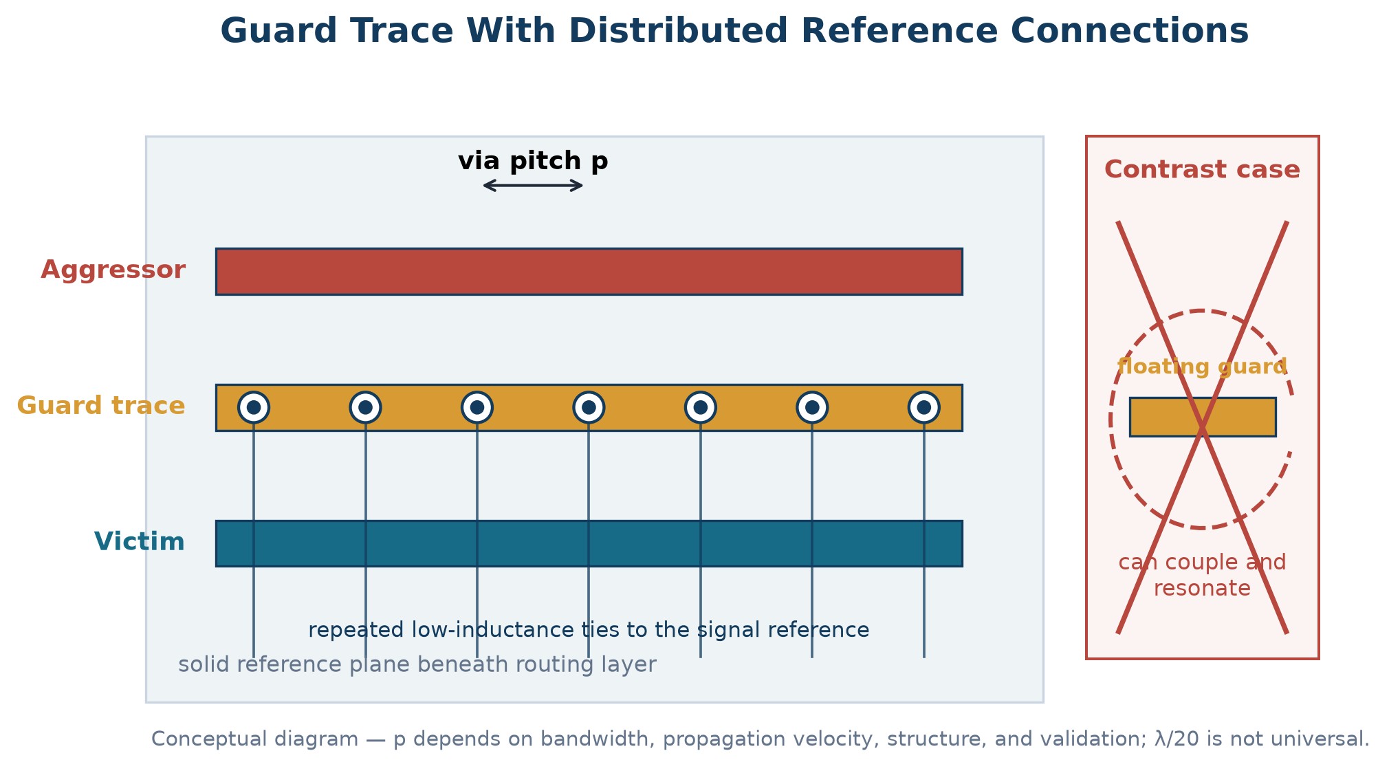
Figure 7. A guard trace needs distributed connections to the signals' reference conductor; a floating guard can become another coupled resonator (conceptual).
Control Edge Rates and Termination
Choose the slowest I/O edge that still meets timing and waveform requirements. Slew-rate controls change the output transition directly. Programmable drive strength changes source impedance and current, so it can alter edge rate, reflections, and crosstalk together. Either setting needs an eye and timing check across process, voltage, and temperature.
On a point-to-point line with a high-impedance load, let the terms below denote driver output resistance, added source-series resistance, and target single-ended characteristic impedance. A common source-termination condition is:
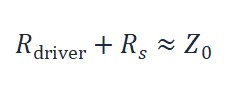
The returning load reflection is then absorbed at the source. Multidrop, bidirectional, fly-by, and heavily loaded DDR nets require topology-specific analysis. The resistor may soften an observed edge as a secondary effect, but it is not a substitute for controlled slew. TI separately documents source termination for reflections and slower rise time for coupled-noise reduction.SPRU889
Termination also changes the impedance seen by a coupled wave on the victim. Model both ends of aggressor and victim lines, including package and receiver capacitance, before selecting a resistor solely from a crosstalk waveform.
FAQ about Crosstalk in PCB Design
Q: Is Crosstalk Determined by Clock Frequency?
No. Clock or data rate affects how often transitions occur, but rise and fall time largely determine the high-frequency content of each edge. A low-frequency control net with a fast buffer can disturb a nearby sensitive net.
Q: What Is the Difference Between NEXT and FEXT?
NEXT is observed at the victim end adjacent to the aggressor source; FEXT is observed at the opposite end. NEXT is associated with backward coupling and reaches a geometry-dependent plateau for a sufficiently long uniform region. FEXT depends strongly on coupled length and even/odd-mode velocity mismatch.
Q: Does Stripline Eliminate FEXT?
Not universally. Ideal symmetric stripline in a homogeneous dielectric can produce strong cancellation of electric and magnetic far-end contributions. Real boards have dielectric, geometric, and termination asymmetries, so some FEXT may remain.
Q: How Much Spacing Is Needed to Reduce Crosstalk in a PCB?
There is no universal spacing value. Start with a documented 3W, 5W, or spacing-to-plane-height heuristic, then evaluate the actual stackup, edge rate, parallel length, terminations, and noise budget. Critical channels should be simulated or measured.High-Speed PCB Layout for PCIe Gen 5
Q: Can a Guard Trace Make Crosstalk Worse?
Yes. A floating or sparsely referenced guard can couple to both neighboring signals and resonate. Increase spacing first; if a guard is still needed, stitch it to the signals' reference conductor at a pitch justified by the relevant frequency range and verify it electromagnetically.
Conclusion about Crosstalk in PCB Design
Crosstalk begins with a transition on the aggressor. Changing voltage and current create electric and magnetic fields; mutual capacitance and inductance couple part of that energy into the victim; the resulting waves appear as NEXT and FEXT and may then reflect. Edge rate, cross-section, coupled length, return path, driver, victim loading, and termination all shape the observed noise.
The most reliable layout strategy is to reduce mutual coupling before fabrication: add spacing, keep critical traces close to continuous reference planes, avoid unnecessary continuous adjacency, and select an appropriate layer geometry. Use guard traces only when their grounding is engineered, and treat 3W, 5W, 3H, and lambda-based via pitches as screening rules rather than proof. For dense or low-margin interfaces, coupled-line simulation with the real stackup and I/O models is the check that turns a plausible rule into a defensible design.
If routing density or interface speed makes those trade-offs difficult, JLCPCB's professional PCB layout service can help implement a crosstalk-aware stackup and routing plan before the design reaches fabrication.
Keep Learning
SFP Pinout Explained: PCB Layout & Design Guide
Key Takeaways The SFP pinout follows a standard 20-pin edge connector, with dedicated pins for power, ground, differential data pairs, and I2C control signals. The Tx and Rx differential pairs carry the high-speed optical or copper signal and need controlled 100 ohm differential impedance through the entire routing path. Low-speed control pins (TX_FAULT, TX_DISABLE, MOD_ABS, LOS, Rate Select/RS1) use standard single-ended routing and don't need impedance matching. Placing the SFP cage near the board e......
DDR5 PCB Layout Guidelines: Design Rules and Best Practices
Key Takeaways DDR5 raises the stakes on layout: 1.1V rails and data rates up to 8800 MT/s leave far less margin for error than DDR4 did. Target around 40–45 Ω single-ended for DQ/CA and 80 Ω differential for CLK/DQS — exact values come from vendor guidelines — and hold them through every via and connector. Keep DQ and DQS length matching within about 5 mil per byte lane, and never route a DDR5 signal over a gap in its reference plane. Plan for 8 to 12 layers with dedicated ground references next to ev......
Via Stitching in PCB Design: A Complete Guide
Key Takeaways Via stitching bonds same-net copper across layers with repeated plated vias, most often ground, to cut high-frequency impedance between regions. A grounded via next to a signal layer transition gives return current a short local path and helps confine the field around the via. Via fences along board edges and RF cavities suppress edge radiation, but their isolation is geometry- and frequency-dependent, with no universal dB value. Keep stitching pitch at or below one-twentieth of the in-b......
Crosstalk in PCB Design: Causes, Types, and How to Reduce It
Key Takeaways Crosstalk starts at an edge: a changing aggressor voltage and current produce electric and magnetic fields that couple energy into a neighboring victim trace. Edge rate matters more than clock frequency alone. A modest-rate bus with fast I/O edges can still create a serious coupling problem. More spacing and a smaller signal-to-reference-plane distance usually provide the cleanest layout improvements, but the result depends on the complete cross-section. NEXT and FEXT do not scale in the......
Mastering IC Board Design: Layout Rules & Best Practices
Key Takeaways Placement is the foundation of good layout. Position ICs, decoupling capacitors, and crystals to minimize trace lengths before routing anything — placement quality determines most of your signal performance. Respect the physics, not just the schematic. High-speed designs demand controlled impedance (e.g., 90-ohm USB differential pairs), length matching, and a well-planned layer stackup to prevent reflections, crosstalk, and power noise. Handle power and heat deliberately. Size power trac......
LVDS PCB Layout Guidelines: Design Tips and Worked Example
Key Takeaways 100 Ω Differential Impedance: LVDS PCB layout starts with one number: 100 Ω of differential impedance. Trace width, spacing, and board thickness all set that number. Route Pairs Together: Route the two traces of a pair together, side by side, and keep their lengths within 5 to 10 mil of each other. Solid Ground Plane: Never let an LVDS pair cross a gap in the ground plane. It breaks the return path and hurts the signal. 4-Layer Minimum: A 4-layer board with a solid ground plane is enough......