JLCPCB Gold Fingers
Last updated on Sep 18, 2026

Gold fingers are the gold-plated columns along the connecting edges of printed circuit boards (PCBs), please see the following picture for reference. Gold fingers are served as the connecting contacts between motherboards and components like graphics or sound cards. PCB gold fingers are also used in various other devices that communicate via digital signals, such as smartphones and smartwatches. Gold is used for the connecting point along a PCB because of the alloy's superior conductivity.
1. Basically, only when ENIG is chosen, the fingers for your PCB will be with gold, if you choose HASL surface treatment, then it will be covered with tin.
2. Chamfers are not available on boards smaller than 5x5cm.
3. If there is fingers in your file and it is panel with v-cut, then the fingers can not be made with chamfer since the fingers will be in the middle of the PCB.
4. During the design stage, sufficient clearance should be maintained between the edge of the gold fingers and the board edge. For designs where the clearance is below the safety distance, our engineering team will optimize the design as necessary. The available bevel angles are 30° and 45°. Compared with a 45° bevel, a 30° bevel facilitates easier insertion and removal. Therefore, we recommend prioritizing a 30° bevel. The details are as follows:
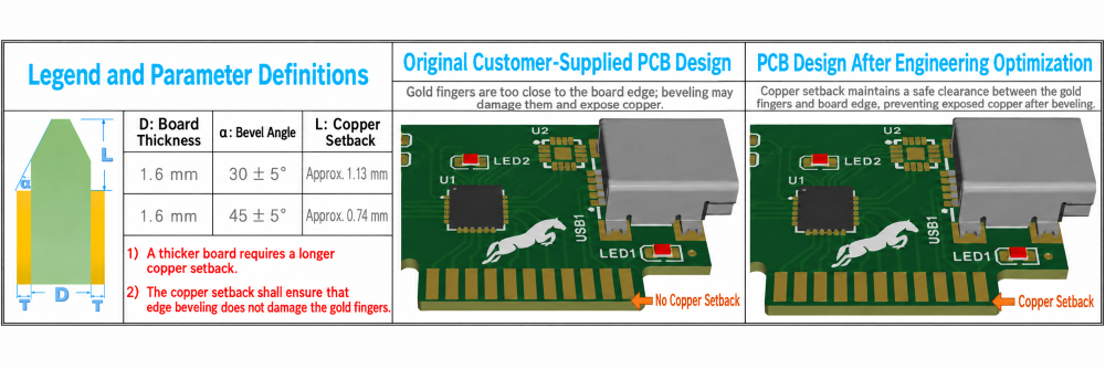
Note: The gold finger area must have the solder mask fully opened (clearance window). For designs without a solder mask opening, JLCPCB will automatically apply a solder mask opening by default. This is to prevent ink from affecting the flatness of the gold finger surface. In addition, repeated insertion and removal may cause the ink to wear off and fall into the card slot, potentially resulting in poor electrical contact.
Example:
The green part is the original Gerber file, while the yellow part is the optimized production file.
The red frame indicates the beveled area. When designing, please kindly pay attention that this area can not have copper. Otherwise, after the bevel, the trace will be damaged and the copper will be exposed.
The length and width of a single board or panel with gold fingers shall not be less than 50mm.