BGA PCB Design Complete Guide: Layout and Routing Guidelines
17 min
- Five Golden Rules for BGA PCB Layout
- BGA Design Parameter Comparison Table
- BGA Layout Guidelines: Pre-Layout Planning
- BGA PCB Layout: Pad, Via, and Escape Strategy
- BGA Routing Guidelines for High-Speed Signals
- BGA Layout Tips for DFM and Signal Integrity
- BGA Layout Verification and Testing
- FAQ about BGA PCB Design

Key Takeaways
Define pad type first: Always confirm SMD or NSMD pad strategy before routing BGA fanout. NSMD is generally preferred for better solder joint formation, while SMD suits very small pads or tight mask registration.
Match the process to the pitch: 0.8 mm BGAs work with dog-bone fanout and standard vias; 0.5 mm BGAs typically need via-in-pad or HDI routing. Picking the right via strategy early saves layers and cost.
Place decoupling capacitors on the bottom side: Mount MLCCs directly under the BGA on the reverse layer to minimize power-loop inductance. Design fanout and decoupling placement together, not sequentially.
Keep high-speed return paths continuous: Route differential pairs over unbroken ground planes. When layer transitions are unavoidable, add nearby ground return vias to maintain the reference.
Run manufacturer-specific DFM before Gerber submission: Check trace/space, BGA pad-to-trace clearance, solder mask bridges, via-in-pad fill/cap notes, and silkscreen clearance against the fabricator's actual process capabilities.
Five Golden Rules for BGA PCB Layout
- Always define SMD or NSMD pad type before routing.
- Match trace length within mils for critical differential pairs, unless the interface guideline gives a different tolerance.
- Place decoupling capacitors as close as possible to the BGA power pins.
- Use via-in-pad for pitches when escape channels are limited.
- Run DFM checks before submitting; solder mask opening and pad-to-trace clearance errors are common BGA yield risks.
BGA Design Parameter Comparison Table
Before routing a dense BGA, the layout rules must be checked against the real manufacturing capability of the board house. JLCPCB lists rigid PCB support up to 32 layers, controlled impedance for several multilayer counts, 1 oz multilayer trace/space down to 0.09/0.09 mm, and notes that 3 mil traces are acceptable in BGA fan-outs. It also lists a minimum via hole/via diameter of 0.15/0.25 mm and specific BGA constraints such as 0.2–0.25 mm BGA pads requiring ENIG and BGA pad-to-trace clearance of at least 0.1 mm, with 0.09 mm locally allowed for multilayer boards. JLCPCB PCB capabilities
| Via strategy | Trace / spacing | Mask / finish | Recommended escape | |
|---|---|---|---|---|
| 0.80 mm | Dog-bone fanout. Prefer 0.20/0.45 mm via where space allows; 0.15/0.25 mm minimum possible when needed. | 0.10/0.10 mm on standard 2-layer; 0.09/0.09 mm on multilayer. 3 mil traces allowed in BGA fanout. | 1:1 pad-to-mask opening possible; keep mask/trace clearance within JLCPCB rules. | Use dog-bone fanout on all rows. Standard process. |
| 0.65 mm | Use smaller vias carefully; 0.15/0.25 mm may be needed. Check annular ring and via-to-track clearance. | 0.09/0.09 mm multilayer preferred. Avoid minimum rules outside the BGA field. | Use tight BGA mask expansion and verify solder-mask bridge capability. | Dog-bone for outer rows; selective via-in-pad for inner rows where channel space runs out. |
| 0.50 mm | Via-in-pad or filled/capped via is usually preferred. JLCPCB via-in-pad supports compatible via diameters from 0.15–0.55 mm. | 0.09/0.09 mm multilayer; 3 mil local fanout where required. | 0.20–0.25 mm BGA pads require ENIG. Keep BGA pad-to-trace clearance ≥0.10 mm; 0.09 mm locally on multilayer. | Via-in-pad for inner rows; dog-bone for outer rows where possible. |
| 0.40 mm | Microvia or advanced via-in-pad planning is usually required. Confirm process before locking stackup. | Use advanced DRC. Route only critical BGA areas at minimum trace/space. | Very tight solder-mask registration; avoid fragile mask slivers. | HDI / microvia escape; expect higher fabrication cost and longer lead time. |
For standards alignment, use IPC-7351 for surface-mount land pattern design, IPC-2221 as the generic printed board design standard, IPC-2152 for current-carrying conductor sizing, and IPC-7095 for BGA design, assembly, inspection, repair, and reliability guidance.
BGA Layout Guidelines: Pre-Layout Planning
A good bga pcb begins even before the first trace is drawn. Pre-layout planning determines if the board can be sold out without problems, and if it can, how much time it will take and how many times it will need to be respinned during the fabrication process.
Stackup Selection and Layer Count for BGA PCB
The number of layers is the first decision that will need to be made in BGA PCB design, when detailing the cost versus density. A 0.8 mm BGA can be considered for a 4-layer or 6-layer stackup, while a 0.5 mm BGA is typically better suited for a 6-layer, 8-layer or HDI plan. While rigid PCB fabrication at JLCPCB supports up to 32 layers and controlled impedance on several layer counts, the number of layers should be as low as is safely maintained for cost control.
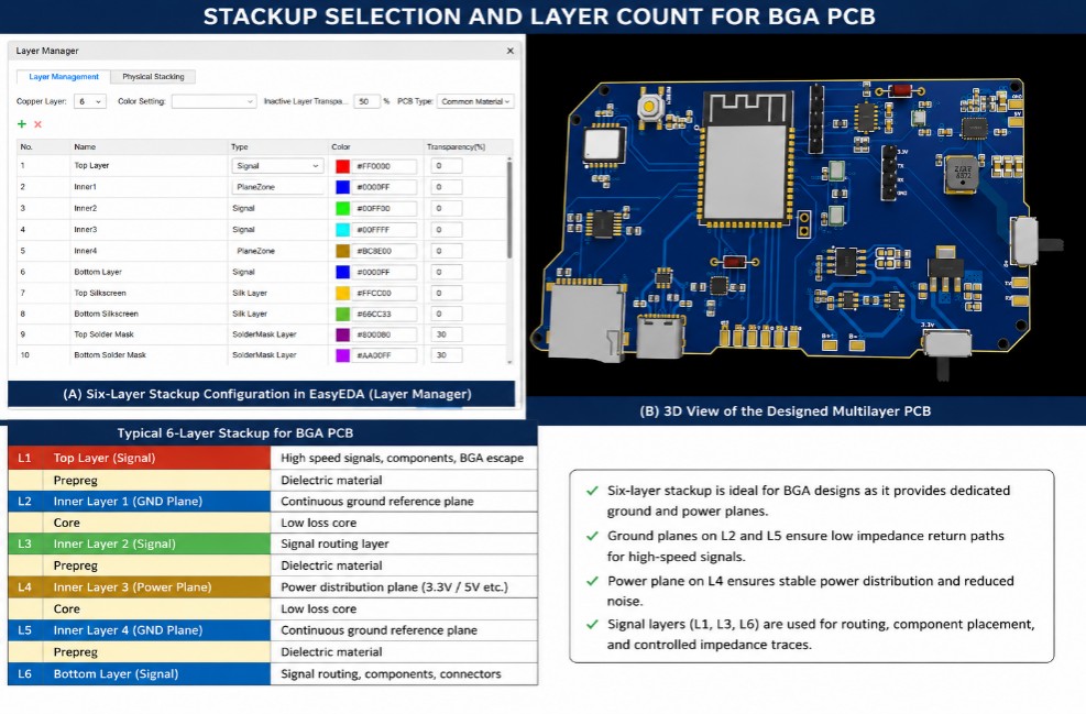
Use the stackup decision to balance escape routing, ground reference continuity, and fabrication cost.
A cost-optimized design begins by calculating the number of routing channels required between BGA balls. The cost saving can be substantial if the design can be reduced from 8 layers to 6 layers without violating the impedance and return path requirements. JLCPCB Layout Service is here to help: Even before routing, the layout team can do a layout evaluation on package pitch, pin map, interfaces and stackup, rather than finding out the problem after Gerber export.
BGA Placement and Orientation Rules
Align BGA with the densest interfaces towards their destination. The direction of DDR pins should be towards memory; high-speed serial pins towards connectors/Phy; power pins towards the cleaner power-plane entry. Rotate the component early if it decreases the number of layer transitions, or layer count to complete the escape of all signals.
Thermal and Mechanical Constraints
The BGA packages have solder joints concealed beneath the package body, and thermal and mechanical reliability must be built into the packages. Distribute heat via thermal vias, internal copper planes and broad power regions. Do not cut ground planes under hot or high-speed regions without electrical justification, and incorporate board-level stiffening structures if large BGA packages cause local board flexure.
BGA Layout for 0.5 mm Pitch: Special Considerations
The common problem in the use of BGA is the pitch of 0.5 mm during casual routing. The available channel between the pads is small, fragility of the mask bridges and as the main routing decision via placement. JLCPCB says via-in-pad can help increase routing density, and that a 4+ layer routing design may not be necessary for a 0.5mm pitch BGA with via-in-pad. If using via-in-pad, the ENIG surface finish is required for BGA pad diameters in the 0.2 mm to 0.25 mm range.
Use ENIG for this class of bga pcb when the diameter of the pad is in the BGA range between 0.2 mm and 0.25 mm, and verify pad-to-trace clearance, and do not use default CAD rules. The routing rules should be configured based on the package pitch, selected finish, via structure, and JLCPCB process parameters.
BGA PCB Layout: Pad, Via, and Escape Strategy
Once you have decided on the stackup structure, the next significant choice is pad and via architecture. This part provides control of solder joint reliability, escape density, and ease of board passing DFM.
SMD vs NSMD Pad Design
SMD pads have the solder mask opening as the solderable area. NSMD pads will reduce the size of the copper pad relative to the solder mask opening allowing solder to wet around the edge of the copper. Key reference IPC-7351 is the surface mount land pattern design, which is applicable with BGA and QFN land pattern.
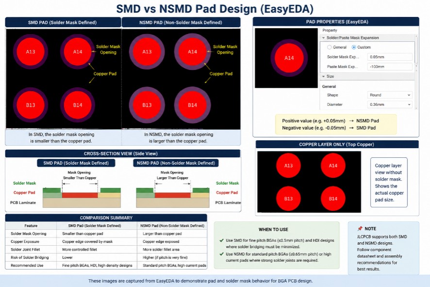
SMD and NSMD BGA pad definitions affect solder wetting, mask registration, and pad anchoring.
NSMD is often the preferred option for most BGA solder balls as it causes the solder to wrap around the edge of the pad, and the process typically results in better joint formation. SMD can be helpful when the pad is very small, mask registration is very tight, or it is important to anchor the pad.
Minimum Trace Width for BGA: Via-in-Pad vs Dog-Bone Fanout
A dog-bone fanout provides a via in the vicinity of the BGA pad and provides a short trace to the BGA pad. Easy and simple when the size of the pitch package is large, it requires surface routing space. In via-in-pad places the via is placed in the middle of the solder pad and the short fanout stub is eliminated, providing a low-inductance path ideal for high-speed and power pins.
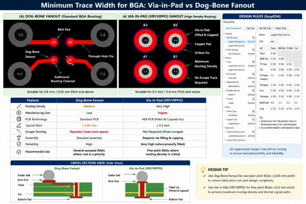
Dog-bone fanout is economical when channel space exists; via-in-pad is cleaner for dense inner rows and fine-pitch BGAs.
Dog-bone fanout is desirable in cases where there is room for the fanout; via-in-pad is cleaner for inner rows where channel space is limited and fine-pitch BGAs. According to JLCPCB, the via-in-pad process fills and plates over vias, epoxy-filled/capped or copper-paste-filled/capped; and compatible via diameters range from 0.15 mm to 0.55 mm. The choice depends on pitch, layer count, and thermal requirements.
This is the type of choice that JLCPCB Layout Service can be helpful. For the layout engineer, he or she can choose which nets to do via-in-pad, which rows to use dog-bone escape, and which minimum design rules to use only for BGA fanout and not everywhere else on the board.
Escape Routing Patterns by Pitch
Escape routes should be considered on a pitch basis and not as a matter of routine. The 0.8 mm BGA can easily pass with the dog bone and conventional via. The tighter trace/space and selective in-pad via may be required for a 0.65 mm BGA. Typically, a 0.5 mm BGA requires via-in-pad or careful HDI routing. And a 0.4 mm BGA generally requires microvias or HDI.
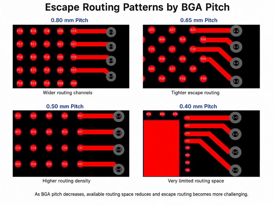
BGA pitch directly affects routing complexity, fabrication process choice, and layout cost.
A complex BGA routing layout is directly related to the complexity of the routing, the selection of the process for the BGA, and the cost of the routing layout. The optimal "path of escape" is not necessarily the one with the least number of layers; it is the one that has the lowest overall risk. A more conservative escape that keeps impedance unchanged and decreases the chance of mask damage can yield better results and lower overall risk.
Decoupling Capacitor Placement: Bottom-Side Layout and Loop Inductance
The power pins of BGA should relate to short and low-inductance current loops. Install the largest decoupling capacitors on the reverse side at the bottom of the board near the corresponding VDD/GND balls. Whenever possible use short via pairs and multiple ground via. Don't use long dog bone power pin fanouts because they will increase loop inductance and minimize decoupling effectiveness.
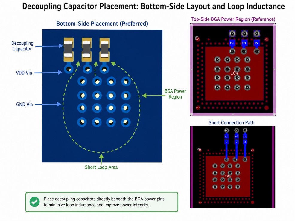
Bottom-side MLCC placement reduces the power-loop area between BGA power pins, capacitors, and ground return.
In dense bga pcb layout, decoupling placement should be done along with fanout. If the bottom layer is already packed with vias, it's the placement of capacitors that will be affected. JLCPCB layout engineers can design the fanout and decoupling at the same time to avoid compromising power integrity.
BGA Routing Guidelines for High-Speed Signals
High speed BGA routing is more than just a pin-to-pin connection. The routing should maintain controlled impedance, continuous return-current paths, and minimize discontinuities and unnecessary via transitions.
Differential Pair and Impedance Control
JLCPCB offers the customer the design information of the impedance and suggests that the customer uses the impedance calculator along with the selected laminate structure to design the line width and spacing. The controlled impedance tolerance is also specified on the capability page for supported stackups as ±10%. For more details, refer to the JLCPCB stackup guide.
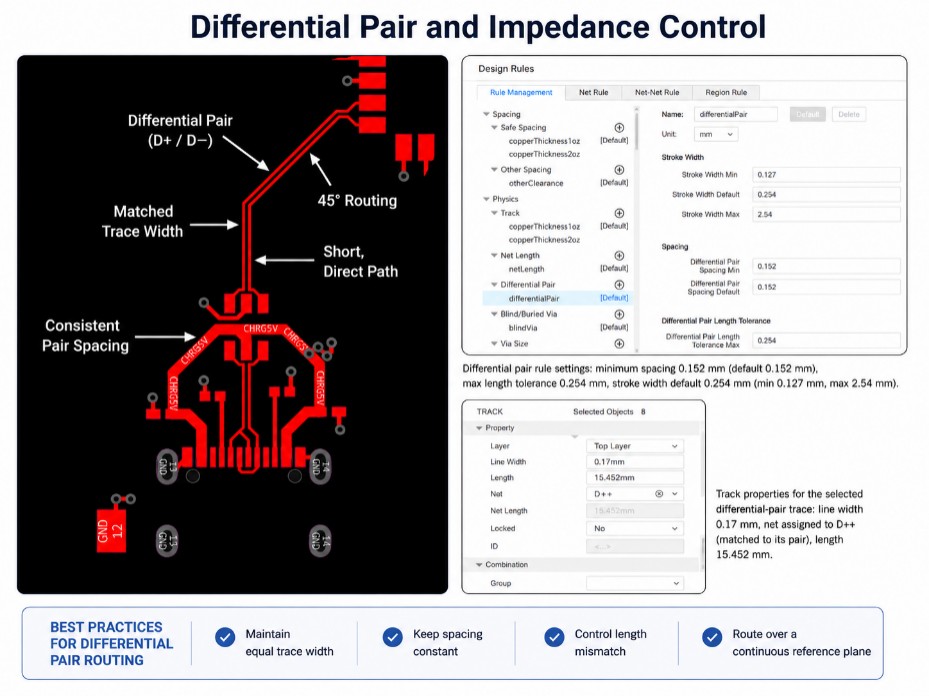
Differential pairs need controlled spacing, matched transitions, and an uninterrupted ground reference.
Length Matching and Skew Management
Length matching is not a feature that should be used in all interfaces. Different timing budgets for USB, PCIe, MIPI, DDR and LVDS. Match intra-pair skew first; match bus groups if necessary for the interface. Tune structures outside the tight BGA field, if possible, to keep them from interfering with the escape routing of main signals.
Power and Ground Plane Strategies
Don't rely on solid ground planes at layers below critical BGA layers. Power planes should be wide and stable but should not divide the return path of high-speed signals. Try to avoid sending high-speed signals across separate planes. If a split cannot be avoided, make an obvious return route by adding stitching capacitors or extending the reference island. Ground planes should be continuous where they are used as the reference for impedance lines.
For high-current rails, use IPC-2152 methodology to size conductors based on current, temperature rise, copper thickness, vias, planes, and board material.
BGA Layout Tips for DFM and Signal Integrity
DFM is not a final checkbox; it is part of BGA routing strategy. Every tight trace, via, pad, and solder mask decision should be checked while the layout is still flexible.
Design Rule Check Essentials
Use the manufacturer constraints to run DRC, not just the generic CAD constraints. The minimum parameters to check are trace/spacing, via hole and via diameter, annular ring, BGA pad-to-trace clearance, solder mask opening, solder mask bridge, via-in-pad fill/cap notes, via silkscreen clearance, and controlled impedance tolerance.
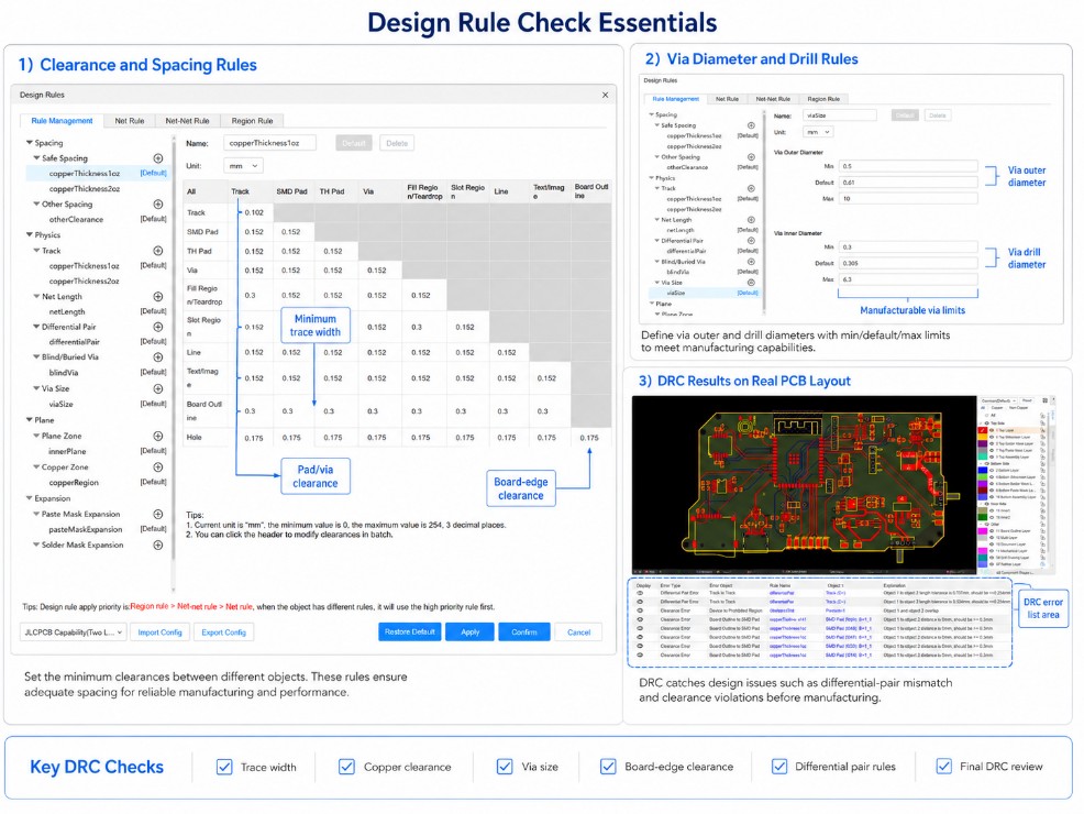
A practical BGA DFM checklist should be completed before Gerber submission.
At JLCPCB, Layout Service not only completes the wiring process but also uses multiple DFM rules to systematically check the reliability of BGA soldering. This helps to avoid short circuits and poor solder joints from the outset, ensuring high first-pass yield.
Thermal Relief and Heat Dissipation
Thermal relief should be used carefully around BGA power and ground pins. Excessive thermal relief can increase electrical and thermal impedance, while direct copper connections can make assembly more demanding if copper is unbalanced. For high-power BGA devices, combine thermal vias, power planes, and large copper areas without introducing assembly issues.
If using via-in-pad for thermal paths, clearly specify the fill and cap process in the fabrication notes. JLCPCB's via-in-pad documentation explains that VIPPO uses filled, plated, and planarized vias so the solderable surface remains flat.
Common BGA Layout Mistakes to Avoid
Mistakes to Avoid
- Using the footprint defaults without checking SMD/NSMD pad strategy.
- Placing decoupling capacitors too far from the related BGA pins.
- Using minimum trace/space everywhere instead of reserving it for BGA fanout.
- Routing high-speed pairs over split planes.
- Forgetting return vias near signal-layer transitions.
- Leaving via-in-pad requirements out of fabrication notes.
- Creating solder mask slivers between fine BGA pads.
- Submitting Gerbers without manufacturer-specific DFM review.
BGA Layout Verification and Testing
Even a clean-looking BGA PCB layout should be verified through design review, DFM checking, and inspection planning. BGA failures are often hidden under the package, so the verification strategy must account for invisible solder joints.
X-Ray Inspection and AOI
AOI can inspect visible components, polarity, solder paste, and placement quality, but it cannot fully inspect hidden BGA balls. X-ray inspection is the preferred method for checking BGA solder joints, voids, shorts, opens, and via-in-pad filling issues after assembly. IPC-7095 is the appropriate standard for BGA inspection and acceptance criteria.
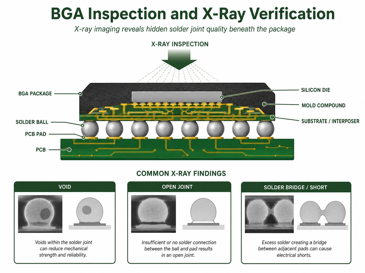
BGA inspection and X-ray verification.
Simulation Tools for Pre-layout Validation
Use impedance calculators for initial trace geometry, then use signal-integrity simulation when edge rates, data rates, or via transitions justify it. For power integrity, estimate target impedance, decoupling network behavior, and current paths before layout. Simulation does not replace DFM review, but it can prevent the three most expensive BGA problems: wrong via strategy, insufficient decoupling, and broken return paths.
Rework Considerations and Cost of BGA Respins
BGA rework is expensive because the joints are hidden, heat must be controlled carefully, and board warpage can damage nearby components. A respin cost more than the PCB price; it costs assembly time, engineering time, schedule delay, and sometimes customer confidence.
Every BGA respin is a preventable cost. If you manufacture your PCB/PCBA with JLCPCB, we'll conduct a comprehensive DFM review before releasing the final deliverables, ensuring optimal manufacturability and minimizing production risks — so your first board is your best board.
FAQ about BGA PCB Design
Q: Can beginners design a BGA PCB?
Yes, but beginners should start with larger-pitch BGAs such as 0.8 mm or 1.0 mm. Fine-pitch packages such as 0.5 mm and 0.4 mm require stricter stackup, via, solder mask, and routing control. A beginner can still complete the design by using manufacturer rules, EasyEDA DRC settings, and a layout review service to compensate for experience gaps.
Q: Is via-in-pad always required for BGA routing?
No. Larger-pitch BGAs can often use dog-bone fanout with standard mechanical vias. Via-in-pad becomes important when the pitch is fine, inner rows cannot escape, or high-speed/thermal performance benefits from shorter transitions. It adds process cost, so it should be used where it solves a real routing problem.
Q: Which surface finish is better for BGA: HASL or ENIG?
ENIG is usually preferred for fine-pitch BGA because it gives a flatter surface than HASL. JLCPCB specifically notes that 0.2–0.25 mm BGA pad diameter requires ENIG. For larger and less dense packages, the finish choice depends on pitch, assembly process, cost, and reliability requirements.
Q: Why do BGA boards need X-ray inspection?
BGA solder joints are hidden under the package body, so normal visual inspection cannot confirm every solder ball. X-ray inspection can reveal shorts, opens, voids, head-in-pillow defects, and solder wicking into vias. This is especially important for via-in-pad and fine-pitch BGA assemblies.
Q: How can I reduce BGA PCB prototype cost?
Reduce cost by selecting the lowest safe layer count, avoiding unnecessary HDI features, using via-in-pad only where needed, and keeping most traces above minimum width/spacing. However, do not reduce cost by violating escape, impedance, or solder mask rules.
Conclusion: BGA PCB Design Complete Guide
A successful bga pcb is the result of stackup planning, correct pad definition, realistic via strategy, controlled high-speed routing, and DFM verification. The smaller the pitch becomes, the more the design depends on manufacturer-specific rules rather than generic PCB layout habits.
For engineers, students, startups, and product teams working with fine-pitch packages, JLCPCB Layout Service can reduce risk by aligning BGA layout decisions with fabrication and assembly constraints from the beginning. Instead of discovering pad, solder mask, via, or routing issues after submission, get your design checked against real manufacturing rules before production.
Keep Learning
How to Design a PCB Board: 5 Steps from Schematic to Layout
Designing a PCB board means turning a validated schematic into a manufacturable layout: start with a clean schematic, place components by function and signal flow, route traces with signal integrity in mind, then manage heat and EMI before running design rule checks and exporting Gerber files. Free tools like EasyEDA cover the complete workflow. This guide explains the layout guidelines that matter at each stage, from schematic preparation to thermal management. Introduction Printed circuit board (PCB......
EMI vs EMC: A Full Guide to Detailed Comparison
EMI (electromagnetic interference) is unwanted electromagnetic energy that degrades the performance of electronic devices. EMC (electromagnetic compatibility) is the design discipline that ensures a device works properly in its electromagnetic environment without disturbing other equipment. For PCB designers, the distinction matters because every layout decision — stackup, grounding, component placement, and trace routing — determines how much EMI a board emits and how well it survives it. Introductio......
PCB Design Guidelines 101: Placement and Routing
Welcome to the second article in our PCB design guidelines series. In this article, we will explore the essential PCB design guidelines that are crucial for achieving optimal PCB design performance and functionality. Whether you're an electronics enthusiast, hobbyist, engineer, student, or professional in the field, understanding these guidelines will empower you to create high-quality PCB designs. In this article we will explore foundational principles and best practices in designing printed circuit ......
BGA PCB Design Complete Guide: Layout and Routing Guidelines
Key Takeaways Define pad type first: Always confirm SMD or NSMD pad strategy before routing BGA fanout. NSMD is generally preferred for better solder joint formation, while SMD suits very small pads or tight mask registration. Match the process to the pitch: 0.8 mm BGAs work with dog-bone fanout and standard vias; 0.5 mm BGAs typically need via-in-pad or HDI routing. Picking the right via strategy early saves layers and cost. Place decoupling capacitors on the bottom side: Mount MLCCs directly under t......
The Ultimate Guide to PCB Layout Design
Printed Circuit Board (PCB) layout design is the foundation of any electronic device, from simple gadgets to highly complex systems. PCB layout design is the process of arranging electronic components and routing connections on a board to create a functional and efficient circuit. The goal is to achieve the smallest possible footprint while maintaining signal integrity and ensuring thermal and electrical performance. There is a lot that goes into any engineered circuit board design, from a basic print......
PCB Layout Guidelines for USB Type-C
Introduction to USB Type-C USB Type-C (USB-C) is a universal connection standard used for device connectivity and charging. As the latest evolution of USB interface, USB-C comes with several advantages, including reversible plug orientation, higher data transfer rates, and power output capabilities. Additionally, USB Type-C can transmit audio and video signals and is compatible with various accessories such as monitors, external storage devices, and chargers. Features of USB Type-C Reversible Plug Ori......