Understanding IPC-6012 Standards for High-Reliability Rigid PCB Fabrication
15 min
- Introduction to IPC-6012 in PCB Manufacturing
- IPC-6012 Performance Classes and Rigid PCB Qualification
- Critical Manufacturing Requirements under IPC-6012
- How IPC-6012 Compliance Prevents In-Field Circuit Failures
- JLCPCB's Stringent Quality Control and IPC-6012 Compliance
- FAQs about IPC-6012
- Conclusion
Key Takeaways
- IPC-6012 vs. IPC-A-600: IPC-6012 is the binding specification, while IPC-A-600 is only for visual reference.
- Class 2 vs. Class 3: Class 3 requires thicker copper (25μm vs. 20μm) and zero plating voids.
- Coupon Verification: Quality is tested by microsectioning panel coupons after thermal stress.
- Upfront Callout: Specify the class on drawings upfront; boards cannot be upgraded later.
IPC-6012 is the line on your fabrication drawing that decides what your supplier is allowed to ship. Most designers type "fabricate per IPC-6012 Class 2" and move on. The fab reads that requirement very carefully because it becomes the value inspectors measure against. A bare PCB is not accepted by appearance alone. To verify plated-through holes, the fab cuts a sample hole in half, polishes the exposed cross-section, and measures the copper thickness along the barrel wall.
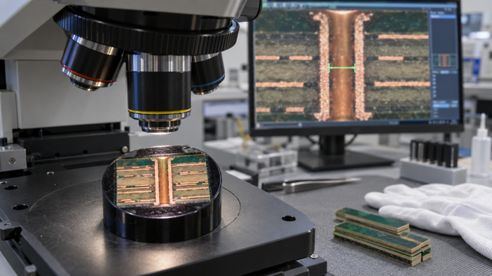
Figure 1: Microsection of a plated through-hole under a metallurgical microscope
Class does not change your design, so a Class 3 board is not a cleverer board. It is the same artwork judged against a narrower window, which is why it costs more and yields less. This guide explains what the current IPC-6012F revision requires and how its three performance classes differ in practical terms. It also shows how IPC-A-600 works alongside IPC-6012 rather than replacing it, so you know what to specify on the drawing to get the performance class you actually ordered.
Introduction to IPC-6012 in PCB Manufacturing
Two documents decide whether a bare board is acceptable, and they do completely different jobs. One sets the numbers your board is measured against, while the other shows what those numbers look like through a microscope.
What is IPC-6012 and Its Core Industry Purpose?
IPC-6012 is the Qualification and Performance Specification for Rigid Printed Boards. It states the measurable requirements a fabricator must meet, so it is the document a buyer invokes when placing an order. The specification exists because "make me a good board" is not a purchasable instruction.
A fab needs to know how thin the copper may get inside a hole before the board is rejected. IPC-6012 answers that with a number, so both sides can measure the same thing and agree. IPC-6012FA covers automotive applications, IPC-6012FS covers space and avionics (both issued in 2024), and IPC-6012EM covers medical devices. If you want the wider picture of how IPC standards shape a PCB layout, the family is worth knowing before you specify one member of it.
IPC-6012 vs. IPC-A-600: Specification vs. Acceptance Criteria
Think of IPC-6012 as the building code and IPC-A-600 as the inspector's photo book. The code states that a beam must carry a specified load, while the photo book shows what a passing beam and a cracked beam look like. Neither replaces the other, and an inspector carries both onto the site.
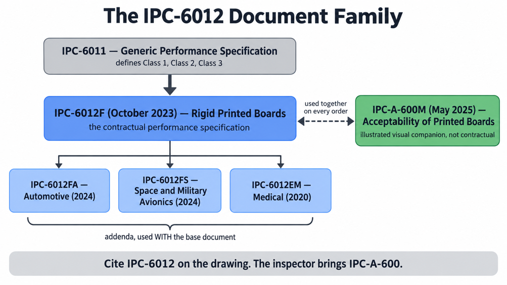
Figure 2: How IPC-6011, IPC-6012 and IPC-A-600 relate to each other
IPC-A-600 is the Acceptability of Printed Boards document, currently in revision M as of May 2025. It is illustrated rather than numeric, so it shows photographs and drawings of acceptable, process-indicator, and nonconforming conditions.
| Aspect | IPC-6012F | IPC-A-600M | What This Means for Your Order |
|---|---|---|---|
| Document type | Performance and qualification specification | Visual acceptability document | Only IPC-6012 is contractual, so name that one |
| Content | Numeric requirements and test methods | Photographs and illustrations of conditions | The numbers you argue over live in 6012 |
| Who uses it | Fab engineering, buyers, quality auditors | Incoming inspectors and line operators | Your drawing talks to the first group |
| Governs | What the board must achieve | What a passing or failing condition looks like | A-600 cannot loosen a 6012 requirement |
| Typical callout | "Fabricate per IPC-6012F Class 2" | Referenced indirectly through 6012 | Never write "per IPC-A-600 Class 3" alone |
IPC-6012 Performance Classes and Rigid PCB Qualification
Performance class is the most consequential word on your fabrication drawing, and it is also the most misunderstood. It describes the service environment the board must survive, so it is not a measure of how carefully anyone works.
Breakdown of Performance Classes 1, 2, and 3
The three classes come from IPC-6011 and run through every IPC performance specification. Each class assumes a different tolerance for failure in service, so the acceptance limits tighten as the consequence of a failure grows. Nothing about the design itself changes between them.
| Class | Name | What the Standard Assumes | Typical Products | What It Means for Your Order |
|---|---|---|---|---|
| Class 1 | General Electronic Products | Function is all that matters; cosmetics are not judged | Toys, remote controls, promotional gadgets | Cheapest and highest yield, rarely worth specifying |
| Class 2 | Dedicated Service Electronic Products | Extended life expected, brief downtime is tolerable | Routers, laptops, and industrial controllers | The sensible default for almost every commercial board |
| Class 3 | High Reliability Electronic Products | Downtime is unacceptable; the board must not fail | Medical devices, avionics, safety systems | Narrower limits, more coupons, higher cost, and longer lead time |
Class 2 is where the vast majority of professional hardware belongs. Reaching for Class 3 without a reason simply buys you a lower yield. Class 3 is not a certificate that a factory holds. It is a build specification that you call out, and the fab agrees to. That means a Class 2 board cannot be promoted to Class 3 after it has been made.
Essential Tests for Rigid PCB Qualification (Thermal Stress and Microsectioning)
Qualification is destructive, which is why nobody performs it on your actual boards. Test coupons are built into the panel border and travel through every step of drilling, plating, and lamination alongside your circuits. Whatever happened to your copper, therefore happened to them.
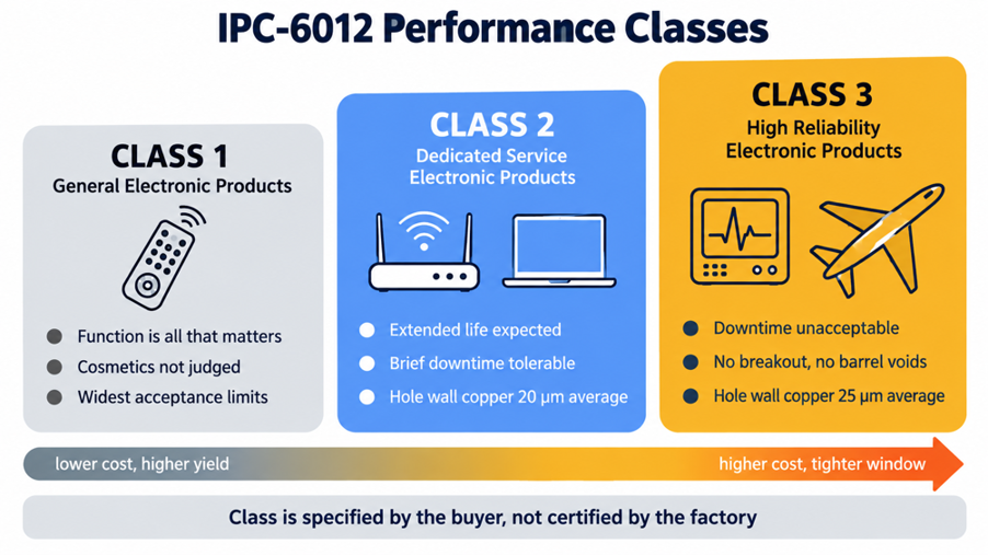
Figure 3: The three IPC-6012 performance classes and where each one belongs
The sequence a fab runs on those coupons follows a fixed order, because each step exists to expose a different failure:
- Cut the coupon from the finished panel and bake it to remove absorbed moisture. Trapped water can turn to steam during heating and create damage that was not present in the original board.
- Apply thermal stress per IPC-TM-650 2.6.8 by floating the coupon in molten solder at 288 ± 5 °C for 10 seconds. This simulates the heat the board may see during assembly.
- Mount, grind, and polish the coupon according to IPC-TM-650 2.1.1 until the center of the selected hole is clearly exposed.
- Measure the hole-wall copper thickness, annular ring, layer-to-hole registration, and dielectric spacing against the limits for the specified IPC class.
- Inspect the polished cross-section for barrel cracks, corner cracks, foil separation, plating voids, and laminate delamination.
Class changes how often this happens rather than how it is done. Class 3 work typically requires microsection evaluation on at least one coupon per production lot, so the evidence is generated continuously rather than once at qualification.
Critical Manufacturing Requirements under IPC-6012
Most of IPC-6012 is a long list of dimensions a finished board must satisfy, but only a handful decide whether it survives service.
Plating Thickness, Annular Ring Width, and Hole Wall Integrity
Hole-wall copper is one of the most important requirements in a plated through-hole. The barrel is essentially a thin copper tube bonded to the resin wall of the hole. When the PCB heats up, the laminate expands much more than the copper, placing mechanical strain on that plated barrel.
If the copper is too thin, repeated thermal cycling can eventually crack the barrel. The result may be an intermittent connection or a complete open circuit. IPC-6012, therefore, specifies two plating measurements rather than one:
- Average thickness: calculated from several measurements taken around the plated barrel.
- Minimum thickness: the lowest individual reading found anywhere on the barrel wall.
Both limits matter. A hole may meet the required average thickness but still fail if one local area is too thin because the plating did not build evenly.
| Requirement | Class 2 | Class 3 | Why the Difference Matters |
|---|---|---|---|
| Hole wall copper, average | 20 µm (0.8 mil) | 25 µm (1.0 mil) | A thicker barrel takes more thermal cycles before cracking |
| Hole wall copper, thin point | 18 µm (0.7 mil) | 20 µm (0.8 mil) | Cracks start at the thinnest ring, not at the average |
| Microvia cap plating | Per class table | 12 µm (0.5 mil) minimum | Protects the target land under stacked via structures |
| External annular ring | 50 µm (2 mil) minimum | 50 µm (2 mil), no breakout | Class 3 removes the drill-wander allowance entirely |
| Internal annular ring | Breakout up to 90° allowed | 25 µm (1 mil) minimum | Drives tighter drill registration and larger inner pads |
| Plating voids in the barrel | Limited voids permitted | None permitted | A void is a stress riser and a corrosion entry point |
The annular ring is measured after drilling, not in your CAD file. The number in your layout is the design ring, and the drill then eats into it by whatever the registration error is. That is the gap annular rings in PCB design have to budget for, which is why a 0.05 mm (2 mil) requirement needs far more than 0.05 mm drawn.
Managing Solder Mask Coverage and Surface Imperfections
Solder mask is treated as an insulating coating with its own performance requirement, not as decoration. IPC-6012 points at IPC-SM-840 for the mask material, and the class you specify selects the mask class. Class 1 and Class 2 boards normally use IPC-SM-840 Class T solder mask, while Class 3 boards default to Class H. Class H is intended for higher-reliability applications and must meet stricter electrical requirements, including a dielectric withstand voltage of at least 500 V.
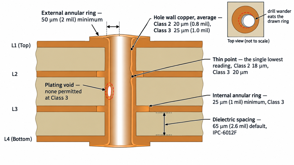
Figure 4: Cross-section of a plated through-hole with measured IPC-6012 dimensions
The conditions a fab actually rejects come down to a short list, so it is worth checking your own artwork against it:
- Conductor width reduction from nicks, pinholes, or edge roughness, measured against the minimum width on your drawing rather than against the neighboring copper.
- Reduced dielectric spacing where an imperfection eats into the gap between two conductors, which is an insulation problem rather than a cosmetic one.
- Mask skips and thin spots over conductors, especially at the knee, where the mask thins as it wraps a trace corner.
- Mask misregistration that exposes copper adjacent to a pad, since that copper will collect solder during assembly.
- Resin recession and voids around the hole wall, which are process indicators at Class 2 and defects once they reach the Class 3 limits.
A mask that looks flawless can still fail an insulation requirement. Copper that looks damaged can still pass, as long as the width and the spacing survive.
How IPC-6012 Compliance Prevents In-Field Circuit Failures
Every limit in the specification traces back to a physical failure somebody once had to diagnose.
Preventing Thermal Shock Damage and Delamination
Copper and epoxy disagree about how much to expand. Copper grows at roughly 17 ppm/°C, while FR-4 grows at around 50 to 70 ppm/°C through its thickness once it passes the glass transition temperature. The resin, therefore, stretches the plated barrel every time the board heats up. A plated barrel may survive one reflow cycle, but damage builds with repeated heating and concentrates at the thinnest copper. That is why IPC-6012 specifies both average and minimum plating thickness. Above the glass transition temperature, laminate expansion rises sharply, increasing stress on the barrel during lead-free reflow.
Delamination is another way thermal stress can damage the board. If moisture trapped inside the laminate turns to steam during heating, it can force the layers apart and create blisters or marring. Poor bonding between the resin and glass reinforcement can lead to the same result. The thermal stress coupon is designed to expose that weakness before production boards reach the customer, so any separation occurs on the test coupon rather than on the finished PCB.
Ensuring Long-Term Reliability for Industrial and Automotive Electronics
Under-hood automotive electronics operate in the harshest thermal environment on public roads. An engine control unit or an ABS module cycles from a -40 °C winter start to well over 125 °C next to a hot engine. The automotive addendum adds requirements around lifted lands and solder mask, both of which are early indicators that the copper-to-laminate bond is losing its grip. A board that passes a generic Class 2 can still fail the addendum.
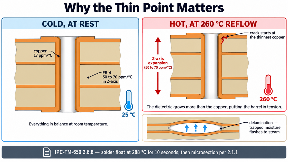
Figure 5: Thermal cycling stress on a plated through-hole barrel
Industrial hardware tends to fail more slowly. A motor drive or factory controller may see fewer extreme thermal cycles, but it operates continuously for years. Long-term mechanisms, therefore, matter more, such as resin recession around plated barrels and corrosion reaching copper through defects in the solder mask.
JLCPCB's Stringent Quality Control and IPC-6012 Compliance
Knowing the specification only helps if the fab you use can actually be measured against it.
Advanced Inspection Processes (AOI, Microsection, and TDR Testing)
Automated optical inspection runs after pattern plating on JLCPCB's line, where a camera scans the board and compares each region against the design data. It catches shorts, opens, nicked conductors, and etch defects on the outer layers. Because it reads reflected light, it measures what sits on the surface, but nothing inside a hole.
Controlled impedance orders add a measurement that maps directly onto IPC thinking. Dedicated coupons in the panel border are TDR-tested, and the standard tolerance is ±10 %, with ±5 % available on request. The coupon principle is identical to the one qualification microsections use, because both judge the panel through a sacrificial strip.
Microsectioning is the destructive counterpart and the only way to confirm hole-wall copper and layer registration. For a fuller comparison of the methods, PCB inspection standards and methods cover where AOI, X-ray, ICT, and functional test each stop being useful.
High-Precision Automated Lines Guaranteeing Class 2 & Class 3 Performance
A PCB manufacturer cannot provide a blanket “IPC Class 3 certificate” for every board it makes. The class applies to a specific build because the requirements are agreed upon before production and verified through inspection and test data from that job. JLCPCB is no different; class compliance has to be tied to the actual board and manufacturing lot rather than treated as a general certification for the factory.
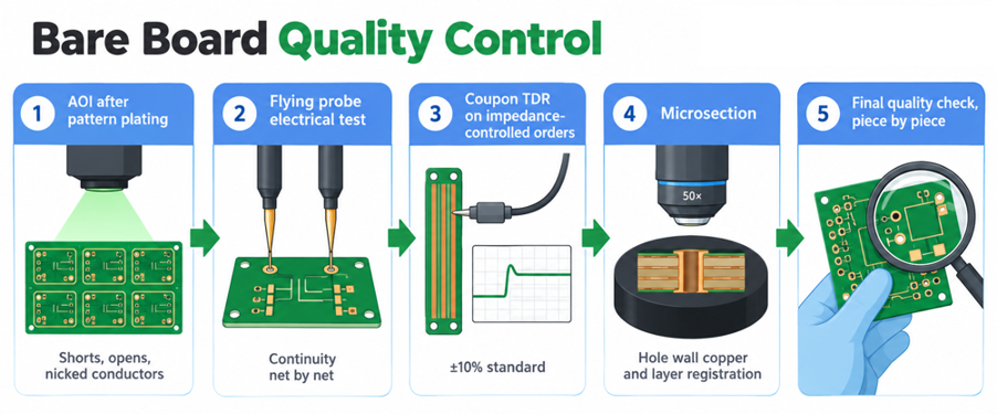
Figure 6: The bare board quality control sequence from AOI to final inspection
The published capabilities give you numbers to compare against. The stated average hole plating thickness is 18 µm. JLCPCB's own plating guide describes hole wall copper as controlled in the 20 to 25 µm range. That sits at or above the Class 2 average of 20 µm. Standard production is therefore a commercial process aligned with Class 2 practice rather than a pre-certified Class 3 line.
FAQs about IPC-6012
Q: Is IPC-6012 Class 3 the same as IPC-A-610 Class 3?
No, because they apply to different products. IPC-6012 Class 3 governs the bare fabricated board, covering copper thickness, annular ring, and hole quality. IPC-A-610 Class 3 governs the assembled board, covering solder joints and component placement.
Q: What happens if I do not specify a performance class at all?
The fab builds to its own standard commercial process, which is generally aligned with Class 2 practice but is not contractually Class 2. You lose the right to reject a board against a specific limit, because no limit was ever agreed upon.
Q: Can a finished board be upgraded to Class 3 after fabrication?
No. Class 3 changes the plating targets, the drill registration allowance, and the coupon sampling before the panel enters production. The evidence, therefore, has to be generated during the build. Inspecting a completed Class 2 board harder does not turn it into a Class 3 board.
Q: Does ordering Class 3 make a marginal design more reliable?
Not on its own, since the standard narrows the acceptance window rather than improving the artwork. If your pads are already too small to leave an annular ring after drill wander, Class 3 raises the rejection rate rather than the reliability.
Q: Do I need to buy the IPC-6012 document to specify it on my drawing?
You can cite it without owning it, and many designers do. Owning a copy matters when you need to argue an acceptance decision, because the exact limits, measurement methods, and allowances live only in the standard itself.
Conclusion
IPC-6012 turns a vague expectation into a purchasable requirement. It states how thin a barrel may get, how much ring must survive drilling, and how a coupon must behave after 10 seconds on molten solder. Every one of those numbers came from a failure somebody had to explain to a customer, which is why the limits look arbitrary until you know the mechanism. The judgment you actually have to make is which class your product earns. Class 2 covers almost all professional hardware, so Class 3 pays for itself only where downtime is genuinely unacceptable.
Revision F has already moved in the designer's favor on dielectric spacing and surface finish defaults. Microvia reliability testing keeps tightening as HDI stackups grow denser. Write the specification, the revision letter, and the class on the drawing, then agree on the coupon plan before release. JLCPCB's published capabilities, certifications, and inspection flow give you concrete numbers to check that callout against, so you are not relying on an assumption.

Popular Articles
• Understanding the Basics of Electronic Devices and Circuits
• Understanding Digital Circuit Timing: Setup Time, Hold Time, Contamination Delay & Clock Skew
• PCBs Explained: A Simple Guide to Printed Circuit Boards
• Guide to the Top 10 Commonly Used Electronic Components
• Digital 101: Fundamental Building Blocks of Digital Logic Design
Keep Learning
A Beginner's Guide to Printed Circuit Board Repair: Common Issues, Methods, and Solutions
Key Takeaways Understand PCB structures, components, and common failure causes to identify repair challenges effectively. Follow a systematic PCB repair process, from fault diagnosis and component replacement to testing and verification. Know when PCB repair is practical and when remanufacturing a new PCB provides a more reliable solution. A printed circuit board (PCB) is a critical part of almost every electronic device. When a board fails, the problem may come from damaged components, broken copper ......
The Hardware Development Process: From Concept to a Finished Electronic Product
Key Takeaways A structured hardware development process turns concepts into functional products through key development stages. Proper PCB design balances performance, manufacturability, and reliability. Early manufacturing considerations help reduce risks and improve prototype success. A reliable PCB partner enables smoother transitions from design to production. Every electronic device you have ever used began as a single idea. A desk lamp that brightens with a tap, a wireless earbud, a controller i......
Demystifying Bare PCB Quality for Reliability-Critical Applications
Key Takeaways Early Defect Catching: Catching faults at the bare board stage costs only the PCB, avoiding wasted components and rework later. Perfboard Risks: Zero PCBs lack reference planes and plated holes, causing signal noise above 10–20 MHz and pad lifting. Critical Material Specs: Reliability depends on hole barrel copper (20–25 µm), Tg, Td, and CTI ratings matching your operating environment. Finish & Shelf Life: HASL and ENIG last ~12 months, while OSP and Immersion Silver/Tin expire in ~6 mon......
A Comprehensive Guide to Capacitor ESR: What It Is, Good Values, and How to Measure It
Key Takeaways Definition: Capacitor ESR (equivalent series resistance) is the single resistance that represents the losses inside a real capacitor, from its electrodes, terminations, electrolyte, and dielectric. Why It Matters: Ripple current flowing through the ESR produces a ripple-voltage step on the supply rail and I²R heating in the capacitor, which limits the capacitor's ripple-current rating and service life. Conditions Matter: ESR varies with frequency, temperature, capacitance, case size, and......
Understanding IPC-6012 Standards for High-Reliability Rigid PCB Fabrication
Key Takeaways IPC-6012 vs. IPC-A-600: IPC-6012 is the binding specification, while IPC-A-600 is only for visual reference. Class 2 vs. Class 3: Class 3 requires thicker copper (25μm vs. 20μm) and zero plating voids. Coupon Verification: Quality is tested by microsectioning panel coupons after thermal stress. Upfront Callout: Specify the class on drawings upfront; boards cannot be upgraded later. IPC-6012 is the line on your fabrication drawing that decides what your supplier is allowed to ship. Most d......
Mastering PCB Plating Types and Process Control in High-Yield Fabrication
Key Takeaways Two-Step Plating: Chemical seed layer comes first, electrolytic copper adds structural strength. Process Choice: Pattern plating enables fine tracks; panel plating suits heavy copper. Via Integrity: Keep aspect ratio ≤ 10:1 to prevent thinnest-point barrel cracking. Surface Finishes: Use ENIG for flat BGA pads and hard gold for high-wear contacts. IPC Standards: Class 2 mandates 20μm copper wall thickness; Class 3 requires 25μm with zero voids. PCB plating turns a stack of drilled lamina......