How to Master PCB Impedance Testing for High-Speed Designs
14 min
- Introduction to PCB Impedance Control and Testing
- Essential Methods for Impedance Calculation and Measurement
- Practical Steps for Executing a Precise PCB Impedance Test
- Overcoming Common PCB Impedance Test Failures
- JLCPCB's Precision Impedance Manufacturing & Quality Assurance
- FAQs about PCB Impedance Test
- Conclusion
Key Takeaways
- Verification via TDR: Impedance testing uses Time-Domain Reflectometry (TDR) on test coupons to verify high-speed traces.
- Real-World Factors: Actual impedance is shifted by manufacturing variables, including trace undercut, solder mask, and pressed dielectric thickness.
- Design-to-Fab Loop: Use the manufacturer's exact stackup Dk values for layout and TDR reports to refine revisions within $\pm 10\%$ tolerance.
An impedance test can be the difference between a USB 3.0 link that works reliably and one that fails in the field. Your layout tool may predict 50 Ω, but fabrication changes the real geometry. Etching leaves slightly trapezoidal traces; the dielectric thickness varies, and the solder mask can shift the final impedance.
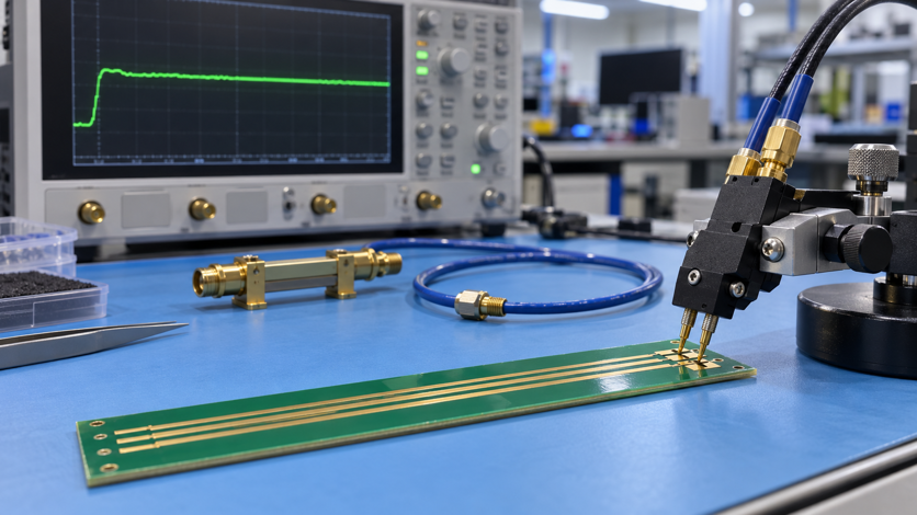
Figure 1: A TDR sampling oscilloscope probing an impedance
The key idea is simple: a fast signal edge responds to the trace geometry directly in front of it. Change the trace width, dielectric height, or material, and the edge sees a different impedance. Any mismatch reflects part of the signal. Impedance testing works by applying a fast electrical step to the trace and measuring the resulting reflections. This guide explains how time-domain reflectometry (TDR) works, how impedance coupons are designed and calibrated, and which fabrication variations can push a 50 Ω trace outside its tolerance.
Introduction to PCB Impedance Control and Testing
Impedance control is what you specify; impedance testing confirms the finished board actually meets it. The two are often confused, but the difference determines whether an impedance problem is caught before or after assembly.
What Is PCB Impedance Test and Why Is It Critical?
A PCB impedance test measures the characteristic impedance of a finished trace. This is the voltage-to-current ratio seen by a fast signal edge as it travels along the copper. It depends on trace geometry and materials, not trace length. Testing matters because impedance is designed in software but created through real manufacturing processes. Etching, dielectric thickness, and material variations can shift the final impedance away from the target.
For example, a 60 Ω trace connected to a 50 Ω source reflects about 9% of the signal. These reflections can create overshoot, ringing, and timing jitter. Impedance testing is therefore the verification step of controlled-impedance PCB design. Resistance testing checks whether a trace is electrically connected; impedance testing checks whether high-speed signals can travel through it cleanly.
Common Applications: High-Speed and RF Circuits
Impedance testing becomes necessary once an edge is fast enough for the trace to behave like a transmission line. The trigger is the edge rate rather than the clock frequency, since a 25 MHz clock with a 500 ps edge already carries energy of nearly 700 MHz.
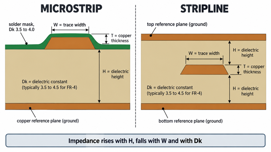
Figure 2: Cross-section of microstrip and stripline showing impedance variables
Reflections start to matter when the rise time is shorter than about twice the trace's propagation delay. The interfaces that demand it are already in your pocket and on your desk.
| Interface | Structure | Target Impedance | What This Means for Your Stackup |
|---|---|---|---|
| RF and antenna feed | Single-ended microstrip or CPWG | 50 ohms | Needs a solid, unbroken reference plane directly below |
| USB 2.0 High Speed | Edge-coupled differential | 90 ohms | Tight pair spacing, no plane splits under the pair |
| USB 3.x, PCIe Gen3+ | Edge-coupled differential | 85 to 90 ohms | Thin dielectric to the reference, often 6 layers |
| Ethernet, LVDS, HDMI | Edge-coupled differential | 100 ohms | Wider spacing than USB, length matched within the pair |
| DDR4 data lines | Single-ended over plane | 40 ohms nominal | Wide traces, so budget routing space early |
Essential Methods for Impedance Calculation and Measurement
Calculation predicts the required geometry before fabrication. Measurement verifies what the fab actually built. You need both because software cannot account perfectly for every manufacturing variation.
Key Factors Influencing Impedance Calculation
Impedance calculation comes down to four physical variables, plus one that designers routinely forget. The four are all geometry and material, and every solver asks for the same set:
- Trace width: A wider trace couples more strongly to the plane below, which lowers impedance.
- Copper thickness: Thicker copper increases capacitance at the trace edges, slightly reducing the value.
- Dielectric height: The distance from the trace to the reference plane, and the variable with the strongest effect.
- Dielectric constant (Dk): How much energy the material between them stores, so a higher Dk means lower impedance.
The IPC-2141 microstrip approximation makes the relationships visible. Impedance rises as the dielectric gets taller, and it falls as the trace gets wider or as Dk increases. Those three directions are worth memorizing because they tell you which way to move when a board comes back out of band.
Solder mask is often overlooked. Its Dk is much higher than air, so it typically lowers microstrip impedance by about 1–3 Ω. The stripline is largely unaffected because it is already buried in the dielectric. FR-4 Dk also changes with frequency and prepreg glass style, so the exact value should come from the fab's stackup data.
| Prepreg Glass Style | Published Dk | Typical Role in the Stackup | If Your Solver Assumed 4.5 |
|---|---|---|---|
| 7628 | 4.4 | Thick, resin-poor filler between cores | Closest to generic FR-4, smallest error |
| 2116 | 4.16 | General-purpose signal-to-plane spacing | Measured impedance comes back a little high |
| 3313 | 4.1 | Thin dielectric for tight 4-layer stackups | Noticeably high, worth recalculating |
| 1080 | 3.91 | Thinnest option, high-speed inner layers | Several ohms high before a trace is etched |
The spread across that column is the whole argument for naming the prepreg. This is why the layer stackup design for high-speed boards must specify the exact glass type rather than using "FR-4."
How to Test Impedance Using Time-Domain Reflectometry (TDR)
Time-domain reflectometry sends a fast voltage step into one end of the trace and watches the echo. The step generator inside a TDR sampling oscilloscope produces an edge of roughly 20 to 35 ps, because only an edge that fast resolves a short discontinuity. The ratio of reflected voltage to the original step gives the reflection coefficient.
From that, the TDR calculates impedance:
Z = Z₀ × (1 + Γ) / (1 − Γ)
where Z₀ is the 50 Ω reference, and Γ is the reflection coefficient. A positive reflection means higher impedance; a negative reflection means lower impedance.
Coupon Testing vs. On-Board Testing
A test coupon is a small strip of copper built into the panel border. It carries dedicated traces on every impedance-controlled layer, etched and plated in the same bath as your boards, so whatever happened to your copper happened to the coupon. Fabs test the coupon because it can be designed for measurement: long straight traces, generous probe pads, no components, one controlled geometry per line. Cutting a coupon off the panel doesn't damage anything, whereas probing a finished board risks scratching a pad you need.
On-board testing is possible, but it fights you at every step. Production traces are short; they turn corners, pass through vias, and sit surrounded by other copper. The TDR therefore sees a busy trace rather than a clean transmission line.
| Aspect | Coupon Testing | On-Board Testing |
|---|---|---|
| Trace geometry | Long, straight, uniform, built for measurement | Short, routed, via-laden, hard to interpret |
| Measurement accuracy | High, typically within 1 to 2 ohms | Degraded by launch parasitics and nearby copper |
| Board damage | None, the coupon is scrap after the test | Probing risks, scratching pad,s and mask |
| Best use | Batch acceptance and quality certification | Debugging one specific failing link |
| What it proves | The process delivered the stackup | This one net behaves as expected |
The bottom two rows carry the decision. Use the coupon to prove the fab hit your number, and reach for on-board probing only when a specific link is already misbehaving.
Practical Steps for Executing a Precise PCB Impedance Test
Preparing the Test Setup and Calibration
Systems such as the Polar Instruments CITS series automate much of the process, but the basic steps stay the same. Follow them in order, because each step removes an error that could affect the next.
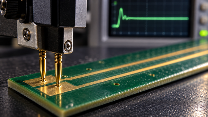
Figure 3: TDR calibration and probe launch on an impedance coupon
- Let the instrument warm up for the specified interval, typically 20 to 30 minutes, because the step amplitude drifts as the sampling head reaches thermal equilibrium.
- Calibrate the vertical axis against known standards, usually a precision 50 ohm air line plus an open and a short.
- Set the horizontal window so that both the launch region and the full coupon trace are visible; you cannot tell a bad launch from a bad trace.
- Land the probe with consistent pressure on clean pads, because a launch carrying extra inductance shows up as a spike.
- Confirm the reference plane is intact under the coupon before trusting a high reading, since a plane gap sharply increases impedance.
Probe launch quality is the largest controllable source of error in the entire procedure. Poor contact adds series inductance, which reads as a positive spike at time zero. If your measurement window starts too early, you average that spike into the result, thereby rejecting a good board.
Analyzing TDR Curves and Impedance Tolerances
A healthy TDR trace has three regions, but only the middle one is used for measurement. The first is the launch region, where probe contact and pad geometry disturb the signal, so it is ignored. The last is the far end, where the trace rises toward an open circuit or falls toward a short, depending on the coupon termination. The useful region is the flat plateau in the middle. The measurement window is placed well away from both ends, typically across about 30% to 70% of the trace length, and the reported impedance is the average over that section.
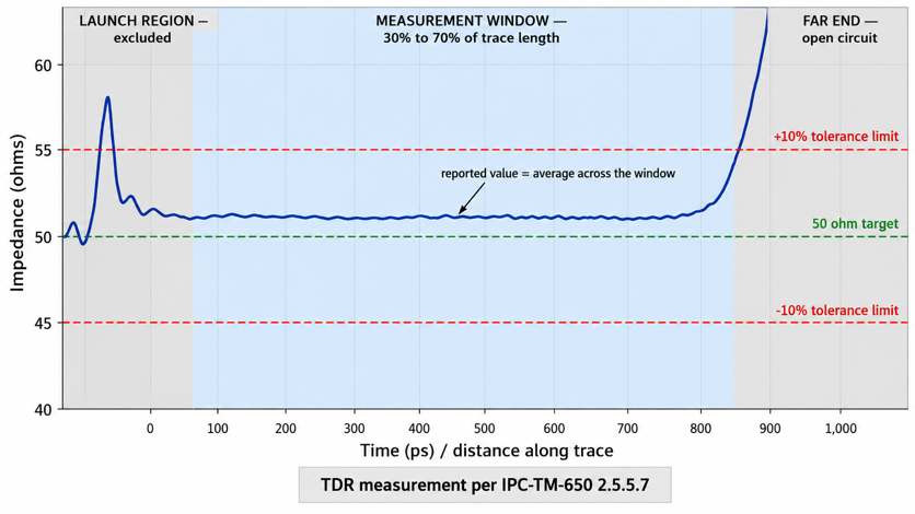
Figure 4: TDR waveform showing the launch region & measurement window
The industry-standard tolerance band is plus or minus 10%, so a 50-ohm target falls anywhere between 45 and 55 ohms. A 100 ohm differential pair passes between 90 and 110 ohms on the same basis.
Overcoming Common PCB Impedance Test Failures
Material and Etching Discrepancies
Copper does not etch into the perfect rectangle assumed by simple field models. Etchant also attacks the trace from the sides, creating a trapezoidal cross-section with a narrower top. For 1 oz copper, this undercut can remove tens of micrometers from the effective trace width. A narrower trace has less capacitance to the reference plane, so its impedance rises—sometimes by several ohms on a thin microstrip.
Outer-layer copper thickness adds another variable. A nominal 1 oz outer layer gains additional copper during plating. Thicker copper tends to lower impedance slightly, while a greater undercut tends to raise it, so the two effects can partly offset each other. This is why fabs refine trace widths using real process data, not formulas alone. Etching also varies across a production panel because spray coverage and copper density are not perfectly uniform. Impedance coupons are therefore placed around the panel to reveal these variations.
Stackup and Dielectric Constant Errors
Prepreg does not maintain the thickness printed on its datasheet. Under lamination, heat, and pressure, the resin flows into the copper topography. The pressed dielectric height, therefore, depends on how much copper sits on the adjacent layers. A signal layer over a mostly empty plane region can end up at a different height than the same trace over a dense area. Since impedance increases with dielectric height, the same net can measure differently at two locations on the same board.
Figure 5: Comparison of designed versus manufactured trace geometry
Dk errors are the other half of the problem, and they are usually communication failures rather than process failures. Suppose your solver used a generic Dk of 4.5 and the fab pressed a 1080 prepreg at 3.91. The field then stores less energy than you modeled, so the impedance comes back high. This is why the fab's published stackup is the input to your calculation, not your library default. It is also why choosing your PCB thickness should come before the impedance target rather than after it.
JLCPCB's Precision Impedance Manufacturing & Quality Assurance
Getting a controlled-impedance board built used to require a phone call and a minimum order.
Advanced Stackup Tools and Free Impedance Calculation
The JLCPCB Impedance Calculator works backward from what you actually know. You enter the layer count, finished thickness, copper weight, target impedance, and the signal and reference layer assignments. It returns the trace width along with the specific stackups that can deliver it. The calculator uses the fab’s actual stackup thicknesses and prepreg Dk values, so its results are more realistic than those from generic formulas.
It supports single-ended and differential traces, with both coplanar and non-coplanar structures. It also suggests suitable stackups, usually listing the lowest-cost option first. Two constraints are worth knowing before you start. Impedance control is available on 4-layer boards and above, because a two-layer construction cannot place a reference plane close enough to the signal. The calculation also assumes the specific laminates JLCPCB uses for that layer count, so you must select the matching material when you order.
Strict Coupon TDR Testing and Quality Certification
Every impedance-controlled order is TDR-tested on dedicated coupons, which sit along the panel border beside your boards. They are etched, plated, and laminated in the same passes as the production panel, so their measured impedance represents what your traces actually received. Each impedance-controlled layer is tested independently. A 4-layer board with controlled traces on both outer layers therefore produces separate results rather than one averaged figure.
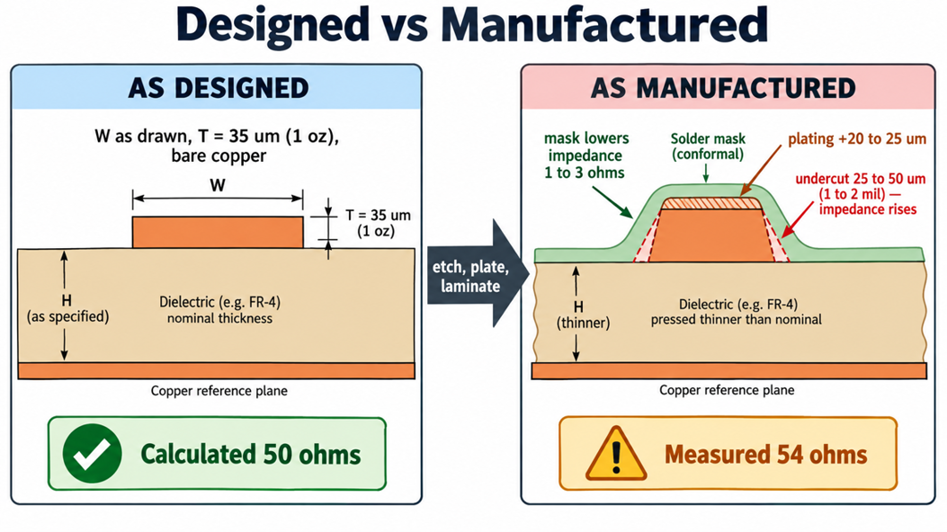
Figure 6: The JLCPCB controlled impedance workflow from calculator to test report
Standard tolerance is plus or minus 10%, with plus or minus 5% available on request where the design genuinely needs it. Results ship with the order on an impedance test report. Traces that came back at 54 ohms against a 50 ohm target passed at the top of the band. A small increase in width in the next revision moves you toward the center, where you have margin on both sides. Treating impedance-controlled routing as a closed loop is what separates a design that passes once from one that passes every batch.
FAQs about PCB Impedance Test
Q: What equipment do I need for PCB impedance testing?
Use a TDR with a fast step generator and a calibrated probe or SMA fixture. Production fabs often use dedicated systems, such as Polar Instruments' CITS series.
Q: Why is my measured impedance lower than calculated?
Common causes include solder mask over outer-layer traces, a thinner-than-expected dielectric, or a higher dielectric constant (Dk). Solder mask alone can reduce impedance by about 1–3 Ω.
Q: Can a 2-layer PCB have controlled impedance?
Generally, no. A standard 1.6 mm 2-layer board has too much spacing between copper layers, requiring impractically wide traces for 50 Ω. JLCPCB also does not offer impedance control on 2-layer boards.
Q: Does trace length affect characteristic impedance?
No. Impedance depends mainly on trace width, copper thickness, dielectric height, and Dk. Trace length affects delay and loss, not characteristic impedance.
Q: Should I always request 5% impedance tolerance?
Usually not. A 10% tolerance is sufficient for interfaces such as USB, Ethernet, and HDMI. A 5% tolerance can increase cost and manufacturing difficulty.
Conclusion
An impedance test closes a loop rather than ticking a box at the end of fabrication. You predict a number in a field solver, and the fab delivers a physical approximation of it through etching, lamination, and plating. TDR on a coupon then tells you how far apart those two ended up.
Undercut raises impedance, solder mask lowers it, and Dk depends on the actual prepreg in the stackup. Once you understand those effects, a TDR report becomes useful design feedback instead of a simple pass/fail result.
As PCIe and DDR edge rates get faster, impedance margin matters more. Using measured data from each revision helps the next design start closer to the target, rather than relying solely on calculations. JLCPCB’s impedance calculator and coupon TDR reports make that feedback loop practical for repeated revisions.

Keep Learning
Why PCB Test Coupons Are Critical for Reliable Board Manufacturing
Key Takeaways Sacrificial Testing: Coupons allow destructive tests without harming active boards. True Process Mirror: They match the exact stackup and density to reflect panel quality. Clean Measurements: Straight lines enable precise TDR impedance and via inspection. Quality Shield: Coupon failures isolate flawed panels before shipping. A PCB test coupon is the one piece of your order that is intentionally destroyed. It rides in the panel border beside your boards, so it sees every drill, plating, a......
How to Master PCB Impedance Testing for High-Speed Designs
Key Takeaways Verification via TDR: Impedance testing uses Time-Domain Reflectometry (TDR) on test coupons to verify high-speed traces. Real-World Factors: Actual impedance is shifted by manufacturing variables, including trace undercut, solder mask, and pressed dielectric thickness. Design-to-Fab Loop: Use the manufacturer's exact stackup Dk values for layout and TDR reports to refine revisions within $\pm 10\%$ tolerance. An impedance test can be the difference between a USB 3.0 link that works reli......
Guardians of Quality: A Complete Walkthrough of PCB Inspection Standards
Key Takeaways Layered Defense: Combining AOI, AXI, ICT, and FCT covers all inspection blind spots. Paste Printing: Solder paste causes up to 60% of defects, making early checks vital. IPC Standards: IPC Class 3 tightens BGA void limits from 25% to 10%, raising costs. Thermal Balance: Equal layout heating balances reflow pull to prevent tombstoning. Design Control: Clear test pads and visible polarity marks ensure reliable automated checks. PCB inspection is not one check performed at the end of produc......
Ensuring Superior Solderability: The Critical Role of Testing in Reliable PCB Production
Key Takeaways Core Purpose: Verifies solder wetting before assembly to prevent yield drops and joint failures. Destructive Test: Per J-STD-002, tested components and coupons cannot be reused in production. Pass Standards: Requires 95 percent solder coverage on leads and 80 percent on exposed thermal pads. Key Defects: Catches non-wetting (exposed metal), dewetting (solder pulling back), and black pad on ENIG. DFM Prevention: Use thermal relief, keep silkscreen off pads, and select the right surface fi......
Solder Joint Inspection in PCB Manufacturing : A Complete Guide to Catching Defects Early
Key Takeaways Solder Joint Inspection is critical in modern PCB manufacturing to catch defects early and ensure product reliability. By combining Solder Paste Inspection (SPI), 3D AOI for visible joints, and X-ray for hidden BGA/QFN issues, manufacturers can effectively detect common defects such as bridging, cold joints, tombstoning, and head-in-pillow. Following IPC-A-610 standards with a layered inspection strategy significantly reduces field failures while improving first-pass yield. JLCPCB’s prof......
3D AOI Inspection Explained : How It Catches Defects That 2D Systems Miss
Key Takeaways 3D AOI Inspection has become essential in modern PCB assembly by using advanced height and volume measurement to detect critical solder defects that traditional 2D AOI systems routinely miss, such as lifted leads, insufficient solder, head-in-pillow, and component coplanarity issues. By delivering precise 3D data through structured light or Moire technology, it significantly reduces false calls, improves first-pass yield, and ensures long-term reliability according to IPC-A-610 standards......