Inside the Factory: A Breakdown of the PCB Manufacturing Process
19 min
- From Gerber to Physical Board: The Architecture of Modern PCB Fabrication
- Core Chemical and Mechanical Stages in the PCB Manufacturing Process
- Surface Protection and Final Finishing Steps
- How Advanced Automation Powers JLCPCB Manufacturing Excellence
- FAQ About the PCB Manufacturing Process
- Conclusion
Key Takeaways
- CAM Prep Prevents Errors: CAM verifies designs against real factory tolerances to catch bad drill files and board outline shorts before production.
- Material Selection Controls Heat: Standard FR4 softens near 130C, while high Tg options stay rigid at 170C for demanding thermal environments.
- Inner Layers Etch First: Cores must be etched and inspected before lamination, as internal traces cannot be reached after pressing.
- Plating Thickness Ensures Reliability: Holes need resin cleaning and multi-step plating to hold 20 microns of copper for thermal durability.
- Surface Finishes Depend on Components: HASL works for basic parts, but tight BGA packages require flat finishes like ENIG to prevent solder bridges.
The PCB manufacturing process turns a folder of Gerber files into a rigid board with copper buried inside it. Between upload and shipping, your design passes through roughly twenty chemical and mechanical stages, and almost all of them happen in tanks you never see. A single bad input costs you the whole batch. An annular ring drawn too tightly becomes a broken hole wall after drilling, so nobody catches the fault until the electrical test.
This guide covers the entire line: CAM checks, inner-layer etch, lamination, drilling, plating, solder mask, and surface finish. You will see what each stage does to your copper, and which design choices decide whether it survives.
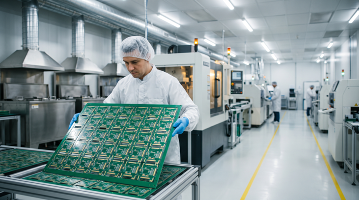
Figure 1: The main stages of the PCB manufacturing process
From Gerber to Physical Board: The Architecture of Modern PCB Fabrication
Your Gerber files are not what the factory actually builds from. A fab first translates them into a tooling package: a panel layout, a drill program, phototools, and an etch compensation table. Most design problems surface right there, because the software compares your artwork against what the chemistry can physically hold.
The order of operations explains almost everything else about the line. A panel is built like a building with the inner floors finished before the roof goes on, so inner layers are etched and inspected before a single hole is drilled. Everything after lamination has to work through a solid board, which is why hole quality and plating dominate the second half of the process.
CAM Data Verification and DFM Preparation
CAM stands for computer-aided manufacturing, and the CAM engineer's job is to make your design buildable without changing what it does. Your files are imported, the layers are put into stack order, and the drill program is matched against the pad artwork. If the drill file calls a hit where no pad exists, the job stops before it costs anyone money. Design for manufacturability checks run next, and they are stricter than the design rule check inside your EDA tool. Your software checks the design against itself, whereas CAM checks it against a real etch line with real tolerances. A clean DRC report can still come back with DFM comments, because the fab is measuring your artwork against equipment rather than against your own rules.
Etch compensation deliberately adjusts the imaging artwork for the side etch that occurs during copper removal. Panel size, process rails, tooling holes, and breakaway features are fabricator-specific, so use the panelization rules supplied with the quotation rather than a generic dimension. Resolve ambiguous drill types, outlines, and copper-to-edge clearances before release; the CAM team should not have to infer design intent.
- Merged plated and non-plated drill files force the fab to ask which holes get copper. A mounting hole and a via look identical in an NC drill file, so the wrong guess plates an M3 hole straight to your ground plane. Export the two hole types as separate files, and the job runs without a query.
- A board outline drawn on the silkscreen or documentation layer leaves the fab without a real profile. CAM then has to rebuild the edge from whatever closed shape it can find. A 0.2 mm (8 mil) error there pushes your mounting holes out of line with the enclosure. Put the outline on a dedicated mechanical layer as one closed polyline.
- Copper poured hard against the board edge gets exposed when the router cuts the profile, and bare copper on a raw edge invites shorts and corrosion. Routing tolerance sits near 0.2 mm (8 mil), so the pour needs to be pulled back at least that far. A 0.3 mm (12 mil) keepout from the outline covers the tolerance with a margin to spare.
Substrate Cutting and Material Selection
Copper-clad laminate is delivered in a large cured sheet of woven glass and epoxy, with copper foil on both sides. It is cut into working panels with a shear or a CNC router, and the edges are beveled so that the sheet does not snag in the conveyorized chemical lines. A thickness, not a weight you could ever feel, is one ounce of copper, which equates to 35 microns (1.4 mil) of foil.
Laminate pulls the moisture out of the air, and the water vaporizes as soon as the press is heated. The panels are then baked at approximately 120 C for 4-6 hours prior to entering the lamination process. Not all FR-4 is the same, and the type you choose will affect the board's characteristics during assembly at the assembly temperature. High Tg (e.g., Shengyi S1000-2M) remains stiff at higher temperatures, around 170 C, while standard FR-4 softens at around 130-140 C – a thick board or one assembled twice is much safer on the high Tg grade.
Four properties decide which laminate belongs under your design:
- Glass transition temperature (Tg): when the resin becomes rubbery. Maintain it at a temperature 20-30 C above the worst-case reflow soak temperature.
- Dielectric constant (Dk): roughly 4.3 for FR-4 at 1 GHz. It sets the propagation delay and the trace width that your controlled impedance needs.
- Dissipation factor (Df): 0.017 to 0.025 for FR-4, against 0.0027 for Rogers RO4003C. Beyond 5 GHz, that becomes a loss.
- Copper foil weight: 1 oz for signal layers, 2 oz once a rail carries more than roughly 3 A.
Board thickness gets chosen at the same time, since it sets both the drill aspect ratio and the dielectric spacing on which your impedance depends.
Core Chemical and Mechanical Stages in the PCB Manufacturing Process
The middle of the PCB manufacturing process is where separate sheets stop being sheets and become one board. Four operations carry the structural load: image and etch the inner layers, press them together, drill through the result, and plate copper down every hole. None of the four can be undone once it is finished, so the tolerances tighten as the panel moves along.
Inner Layer Patterning and Lamination for Multilayer Boards
Inner layers are patterned while they are still separate cores, because once the stack is pressed, there is no way back inside it. Each core is cleaned, laminated with dry film photoresist, and exposed either through a phototool or by a laser direct imaging head. Developing washes off the unexposed resist, and the copper underneath it is then dissolved in the etcher.
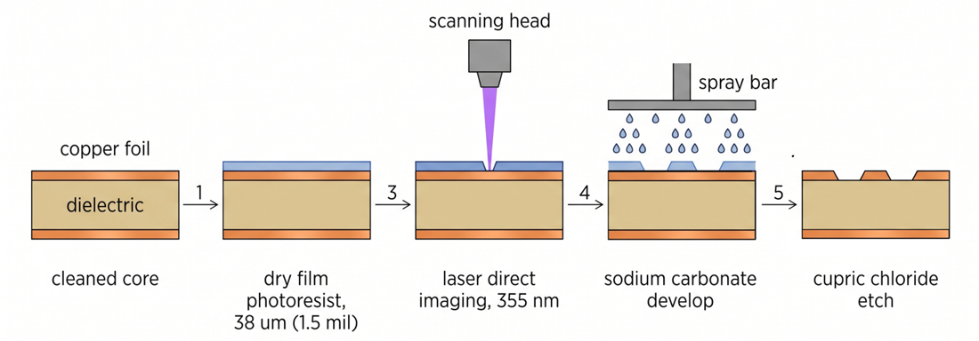
Figure 2: Inner layer imaging and etch sequence
The copper is removed with Cupric chloride or ammoniacal etchant, which is sprayed onto a moving panel under controlled pressure. The chemistry works in all directions simultaneously, and so the trace has sloped sidewalls instead of vertical sidewalls. This slope is referred to as the etch factor, and the typical 1 oz inner layer is close to 3:1, which means that the trace will lose about 12 microns (0.5 mil) on each side. Automated optical inspection of each inner layer prior to it being lost in the stack. The scanner compares etched copper to the CAM image and alerts to shorts, opens, and nicks to approximately 15 microns (0.6 mil). Panels that pass go directly to an oxide or bond enhancement treatment that roughens the copper to give the prepreg resin something to hold on to.
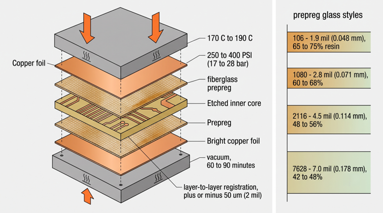
Figure 3: A multilayer lamination stack
The etched cores are joined together in one piece by lamination with prepreg—a partially cured epoxy and glass cloth. The stack is pinned or riveted for registration and put in a heated press. The resin melts when heated, is squeezed under pressure into all the spaces, and hardens. The FR-4 cycles are optimized with a controlled cooling ramp, with a maximum cycle temperature of 250 to 350 psi at 185 C, as a rapid cool will lock stress into the board.
Precision Mechanical PCB Drilling and Laser Micro-Via Creation
Drilling comes after lamination because a through hole has to pass the finished stack in a single pass. Panels are stacked two or three high between an aluminum entry foil and a phenolic backup board. Carbide bits then cut the holes at spindle speeds of 100,000 to 200,000 rpm. The entry foil stops the bit wandering as it bites, while the backup board keeps the exit hole from tearing out.
Aspect ratio is board thickness divided by finished hole diameter, and it affects drilling and plating capability. The permitted ratio depends on the fabricator, material, drill size, plating process, and reliability class. Confirm the finished hole and stack-up with the fabricator before treating a ratio as routine.
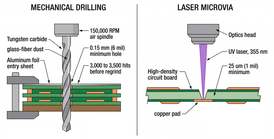
Figure 4: Mechanical drilling and laser microvia formation compared
Laser drilling is the solution when a mechanical bit can no longer be used. One dielectric layer is ablated at a time by a UV or CO2 laser. It creates 75-150 micron (3-6 mil) blind microvias that are terminated on the underlying copper. The depth is self-limiting since the beam will not penetrate copper, which is why stacked and staggered HDI structures can be used. All the smartphone mainboards are wired in this fashion, because it is impossible to escape a 0.4 mm pitch application processor using 0.15 mm through holes.
Panel PCB Plating and Through-Hole Copper Deposition
A drilled hole is a bare tunnel through glass and epoxy, and neither of those conducts anything. Plating exists to line that tunnel with copper so the layers it passes through become a single net. The work is split into two stages because you cannot electroplate onto a surface that carries no current at all.
The panel runs the following sequence, and the order of it is fixed:
- Desmear strips the resin that the drill smeared across the exposed inner layer of copper.
- Electroless copper lays a thin conductive film onto the bare hole wall.
- The panel flash plate thickens that film enough to survive handling.
- Outer layer imaging opens the resist over traces and pads only.
- Pattern plate builds copper to the final thickness and caps it with tin.
- Strip, etch, strip removes the resist, the background copper, and finally the tin.
Desmear is a process in which the melted resin is removed from the exposed inner layer pads by wiping with a drill bit. The epoxy is dissolved in a solvent, then oxidized by alkaline permanganate and neutralized cleanly by a neutralizer. However, if the smear survives, plated copper does not adhere to the inner layer pad but rather to the resin, and this bond becomes open during a few thermal cycles.
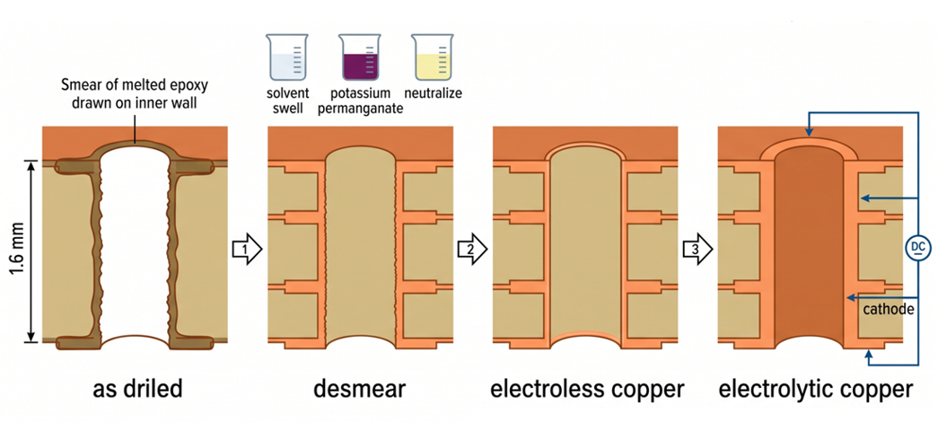
Figure 5: The desmear, electroless copper, and electrolytic plating sequence
Electroless copper is a chemical deposit rather than an electrical one. A palladium catalyst is adsorbed onto the hole wall, and the bath then reduces copper onto that catalyst in the absence of current. The film is only 0.3 to 1 micron thick, which is far too thin to carry current but just conductive enough to electroplate on.
The actual copper thickness is developed by electrolytic plating in an acid copper sulfate bath. Copper grows on all wetted surfaces, including a hole barrel, as the panel becomes the cathode, current flows. IPC-6012 Class 2 requires a minimum of 20 microns (0.8 mil) of copper in the hole, and Class 3 requires a minimum of 25 microns (1 mil) of copper in the hole.
Surface Protection and Final Finishing Steps
The bare copper will start to oxidize as soon as it leaves the etch line, and the oxide will not solder. The finishing half of the line is everything that isn't supposed to be soldered, and the other half is everything that is soldered. The two are always selected together, with solder mask taking care of the first job, and surface finish taking care of the second.
Application and Imaging of the Solder Mask Layer
Solder mask is a liquid photoimageable epoxy, sprayed or curtain-coated across the whole panel and then imaged like a photoresist. The panel is tack dried near 75 C, exposed through the mask artwork, and developed so the ink clears off the pads. A final bake around 150 C for an hour cross-links whatever is left into a hard coating.
Mask coverage is not uniform, and it's not as thick as the datasheet indicates. The ink runs off the top of a trace and puddles next to it. Thus, a 35-micron trace corner can only support 10 to 12 microns (0.4 to 0.5 mil) at its sharpest corner. A dam between two fine-pitch pads should be approximately 0.1 mm (4 mil) wide to survive the development process, as any thinner width will be washed away and allow solder to bridge the pads.
Selecting the Right Surface Finish for Soldering and Storage
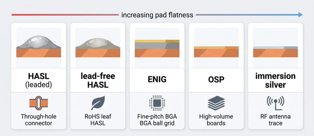
Figure 6: Surface finish comparison showing HASL, ENIG, and OSP pad cross-sections
Surface finish is the coating that keeps exposed copper solderable until the day the board is assembled. Copper grows an oxide within days of leaving the line, and oxide blocks the intermetallic bond that a solder joint depends on. Every finish trades flatness against shelf life and cost, so choose it around your smallest component rather than around your budget.
| Surface Finish | Coating Thickness | Shelf Life | Pad Flatness | Best Used For |
|---|---|---|---|---|
| Lead-free HASL | 1 to 25 microns (0.04 to 1 mil), uneven | About 12 months | Poor | Through-hole parts and passives down to 0603 |
| ENIG | 3 to 6 microns nickel, 0.05 to 0.1 microns gold | 12 to 24 months | Excellent | BGA, QFN, 0.4 mm pitch and press-fit |
| OSP | 0.2 to 0.5 microns (0.008 to 0.02 mil) | About 6 months | Excellent | Cost-driven boards assembled soon after delivery |
| Immersion silver | 0.1 to 0.4 microns (0.004 to 0.016 mil) | 6 to 12 months | Excellent | RF boards and fine pitch on a tight budget |
| Immersion tin | 0.8 to 1.2 microns (0.03 to 0.05 mil) | About 6 months | Excellent | Press-fit connectors and fine-pitch parts |
How Advanced Automation Powers JLCPCB Manufacturing Excellence
Volume manufacturing is a repeatability problem long before it is a precision problem. Hitting 0.09 mm (3.5 mil) trace and space once is a laboratory result, whereas hitting it on every panel of every job is a factory. JLCPCB runs a five-board prototype down the same line as a production order. A hobby project, therefore, comes back with the same registration and plating tolerances as a commercial build.
High-Precision Machinery for Tight Tolerances and High Layer Counts
Layer count is limited by registration rather than by how many sheets a press can hold. Every core has to line up with every other core inside a fraction of a pad, and both copper and glass move slightly during pressing. Laser direct imaging solves half of that, because it scales the artwork per panel to match the material's measured shrinkage.
X-ray drilling targets close the other half of the gap. The machine reads buried registration marks through the laminate, so the drill program shifts to match the panel it is actually holding. Without that correction, a 12-layer board would need loose annular rings everywhere, and you would pay for it in routing space on every single layer.
| Capability | JLCPCB Standard | What It Means for Your Design |
|---|---|---|
| Layer count | 1 to 32 layers on FR-4 | Dense stack-ups do not need a specialty fab |
| Trace and space | 0.10 / 0.10 mm (4 / 4 mil) at 1 oz, 0.09 mm (3.5 mil) on 4+ layers | 0.5 mm pitch BGA escape routing is buildable |
| Minimum via | 0.15 mm (6 mil) drill with a 0.25 mm (10 mil) pad | Fits between 0.8 mm pitch pads without a dogbone |
| Board thickness | 0.4 to 4.5 mm, tolerance ±10% above 1.0 mm | Card-edge and connector fits need that tolerance checked |
| Impedance control | ±10% standard, ±5% on request, 4+ layers | USB and Ethernet pairs hold 90 or 100 ohm targets |
| Surface finish | HASL, lead-free HASL, ENIG, OSP | ENIG for fine pitch, HASL for through-hole, and cost |
Those numbers are the real boundary between a design that quotes instantly and one that comes back with a DFM comment. Staying a little inside each limit is cheaper than sitting on it, because a job at the edge of the process has no margin left when a panel drifts.
Uploading Gerbers to the JLCPCB quote page prices the job against those limits in seconds. The automated DFM report then flags anything the line cannot hold before you pay for it. Two-layer PCBs start at $2, stencils at $6, and standard builds ship in one to two days. An extra design iteration, therefore, costs less than the parts you would populate it with.
Automated Optical Inspection (AOI) and Strict Quality Control
Automated optical inspection photographs the panel under controlled lighting and compares every region against the CAM reference. The camera never gets tired, so its judgment on the four hundredth panel matches its judgment on the first. It works from reflected light, however, which means it can only report what is visible from above.
On a bare board that still covers most of what can go wrong in the copper:
- Shorts and opens between nets
- Trace width or spacing drifting outside the ±20% etch tolerance
- Nicks, pinholes, and mouse bites along a conductor
- Missing, undersized, or misplaced pads
- Drilled holes offset from their pad, eating into the annular ring
- Solder mask misregistered over a pad edge
What AOI cannot tell you is whether a plated barrel stays continuous through the middle of the board. Electrical test covers that, and it is the only stage that verifies the netlist rather than the picture. Flying probe suits prototypes because it needs no fixture, while a bed-of-nails rig is faster once quantity justifies building one.
Destructive testing backs up everything the cameras cannot reach. A coupon from the panel edge is cross-sectioned, polished, and measured under a microscope to confirm the hole wall copper against IPC-6012. Panels are then profiled by router or V-scored, and V-cut depth is checked because cutting too deep leaves a web that cracks during depaneling. The depth limits that keep you inside spec are set out in the JLCPCB V-cut panelization standards.
FAQ About the PCB Manufacturing Process
Q: How long does the PCB manufacturing process take?
A standard two-layer board takes 24 to 48 hours to fabricate. Multilayer boards need 3 to 5 days, because lamination and the extra imaging cycles are sequential steps that cannot be run in parallel.
Q: What is the difference between PCB fabrication and PCB assembly?
Fabrication builds the bare board, covering etching, lamination, drilling, plating, and surface finish. Assembly comes afterward, when components are printed, placed, and soldered onto the finished board.
Q: Why are inner layers etched before drilling?
Inner layers can only be imaged while they are still separate cores. Once the stack is laminated, there is no physical access to it, so all inner-layer patterning and inspection have to finish first.
Q: How thick is the copper plated inside a via?
IPC-6012 Class 2 requires at least 20 microns (0.8 mil) of copper in the barrel, while Class 3 requires 25 microns (1 mil). Most fabs target the middle of that band, since it leaves margin for thermal cycling.
Q: Which surface finish suits a fine-pitch BGA?
ENIG is the usual answer because it leaves a dead-flat pad and maintains solderability for two to three years. HASL is too uneven to trust below about 0.5 mm pitch.
Conclusion
The PCB manufacturing process is a chain of irreversible steps, so your Gerber files are the only place where you influence all of them at once. Etch compensation, aspect ratio, prepreg thickness, and mask dam width all come from numbers you set weeks before a panel is ever cut. Understanding what the line does with those numbers is what separates a design that merely passes DRC from one that yields.
Fabrication is also getting quietly harder as boards get denser, since laser microvias and 0.09 mm geometry leave far less room for a lucky panel. The fabs that keep up are the ones measuring every panel and correcting for it, rather than hoping the material behaves if you want to know how your own design fares against a real process window, upload it and read the DFM report before you commit to a build.

Keep Learning
Understanding SMT PCB Boards Technology: An Essential Component of Modern Electronics
Surface Mount Technology (SMT) has changed manufacturing of modern electronics. It has made designs and assembly methods more efficient. Many modern electronics depend on SMT PCB boards, which make it possible for circuit designs to be small and efficient. This is what today's technology needs. This article discuss about many types of SMT PCB boards, their uses, and the best methods for designing and assembling them. 1. What is an SMT PCB Board? Printed circuit boards called SMT PCB boards, use surfac......
How to Choose the Right Prepreg Material for Reliable Multilayer PCB
Have you ever wondered what makes all those copper layers stick to a cross-section of a multilayer PCB? Prepreg material is the answer, and it is of much more importance than most engineers think it is. Choose the prepreg selection wrong, and you are predetermined to delamination, impedance drift, and long-term reliability problems. Prepreg is not only glue. It is a designed composite that determines your dielectric separation, dictates your impedance, affects signal loss, and determines your board be......
Via Filling Explained: Key Techniques, Benefits, and Solutions for High-Performance PCBs
Key Takeaways Via filling completely fills plated through-holes and microvias with epoxy or conductive copper paste, followed by planarization and copper capping (POFV). It eliminates voids, solder wicking, and thermal/mechanical issues while enabling reliable via-in-pad designs. Benefits include superior heat dissipation (up to 8 W/m·K), better signal integrity, higher mechanical strength, and improved assembly yields. JLCPCB provides free non-conductive filling + POFV on 6+ layer boards. Ideal for H......
How Fiducial Markers Guarantee Perfect Alignment in Professional PCB Fabrication
Today, the most sophisticated pick-and-place machine can place a 0.5 mm pitch QFP on its footprint, board after board, thousands of times, and never miss. It is not only a matter of expensive cameras or high-quality servos, but it begins with a little, very small copper dot, simply hanging there in the corner of your PCB. That dot represents a fiducial marker, and without it, even the smoothest SMT line would be laying components in the dark. The unrecognized heroes of automated assembly are the fiduc......
Technical Guidance: Character Design Specifications
To facilitate component assembly, future maintenance, and traceability of PCB manufacturing information (such as manufacturer, production date, batch number, etc.), various character markings are typically silk-screened onto the PCB. These include component designators, polarity marks, test point labels, company logos, and production traceability information. Traditional PCB character silk-screening uses the screen printing process, hence the term “silk-screen characters.” High-definition characters a......
Step-by-Step Guide to the Printed Circuit Board Manufacturing Process
Key Takeaways Core Role: PCBs provide the physical foundation and electrical connections for modern electronics. Multi-Step Process: Manufacturing spans design imaging, substrate creation, inner/outer layer etching, lamination, and surface finishing. Precision & Quality Control: Features micro-drilling (down to 100 µm) for layer connectivity, Automated Optical Inspection (AOI), and final electrical testing. Protection & Finish: Solder masks and surface finishes (e.g., ENIG, HASL) protect copper traces......