Effective Solutions to Reduce PCB Ground Loop Noise
16 min
- Fundamentals of PCB Ground Loops
- Common Problems Caused by PCB Ground Loops
- How to Prevent Ground Loops: Practical PCB Design Strategies
- PCB Manufacturing Controls That Keep Ground Impedance Low
- FAQs About PCB Ground Loops
- Conclusion
Key Takeaways
- Cause: Multiple ground paths with voltage differences cause hum, ADC errors, and EMI.
- Strategy: Use star grounding for <1 MHz; use solid ground planes for >10 MHz.
- Routing: Never route fast traces across split planes to avoid large return loops.
- Mitigation: Use isolation, differential pairs, and place GND vias/caps close to IC pins.
- Stackup: Use thinner prepreg to lower return loop inductance.
A ground loop occurs when multiple grounds form a closed conductive path, allowing unwanted electrical currents to flow through the ground conductors and cause voltage differentials between circuit reference points. These voltage differences can result in noise that produces 50 Hz or 60 Hz hum, erratic ADC output, and increased electromagnetic interference (EMI). In contrast to an ideal schematic, where all ground symbols are at ground potential, real PCBs have resistance and inductance in the copper traces, planes, and vias.
This guide describes how ground loops form, the impact of common-ground paths on circuit performance, and how to distinguish ground-loop noise from ground bounce. It also addresses real-life noise-reduction techniques, including ground planes, isolation, and via placement.
Fundamentals of PCB Ground Loops
For a PCB ground loop to occur, there must be more than one path for the current to return, and there must be a potential difference between the locations where the current returns. The frequency at which the return current occurs then determines the path the current takes.
What Is a PCB Ground Loop and How Does It Form?
A ground loop is a closed circuit of conducting materials that includes ground connections. It occurs when two circuits have more than one path to a common reference, and the common reference points are not at the same potential. All copper connections have resistance and inductance. When current flows through the copper, it produces a voltage between its ends that is in series with any signal measured across it.
Noise can be coupled into a circuit in two ways by a ground loop:
- Conductive coupling: Return current from one circuit flows through the copper shared with another circuit. That voltage drop changes the second circuit's reference voltage. This is also known as common-impedance coupling.
- Magnetic coupling: A time-varying magnetic flux passing through a closed loop produces a voltage around the loop. The larger the loop area, the more flux is linked; hence, a higher voltage is picked up.
If you connect a board to two mains-earthed devices, such as a bench supply and an oscilloscope, the 50 Hz or 60 Hz hum from both devices can be displayed. There is a voltage difference between the two earth connections when the building's protective-earth system is compromised. The loops created by the cables can also connect mains-frequency magnetic flux.
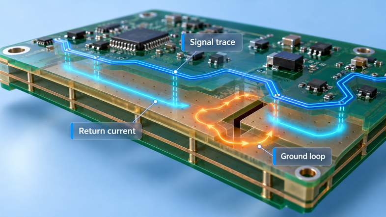
Figure 1: PCB ground loop formed by two earth connections between a sensor board
Single-Point vs. Multi-Point Grounding by Frequency
With single-point grounding, each circuit is connected to a common ground point via its own circuit conductor. The multi-point grounding technique uses a low-impedance grounding plane, with each circuit connected to the closest point on the plane. The right choice depends on the return current frequency at the highest frequency.
Single-point grounding eliminates common-return-path impedance; however, each return conductor has some inductance. By Rosa's formula, the partial self-inductance of a 100 mm trace, width 0.25 mm, without a plane below it, is approximately 140 nH. That's about 9 Ω reactance at 10 MHz.
| Grounding Scheme | Typical Frequency Range | Typical Applications | Layout Consequence |
|---|---|---|---|
| Single-point (star) | Below about 1 MHz | Audio, precision DC measurement, high-current power returns | Run each return to one node on its own short conductor |
| Single-point or multi-point, by conductor length | About 1 MHz to 10 MHz | Mixed-signal boards, chassis connections | Single-point if the longest ground conductor is shorter than λ/20 at the highest frequency |
| Multi-point (plane) | Above about 10 MHz | Digital logic, RF, fast switching edges | Solid ground plane, with a ground via at each component's ground pins |
It is not the clock rate but rather the spectral content of the return current that is important. A 1 MHz clock with nanosecond edges has harmonics well above 10 MHz, meaning the return requires a plane.
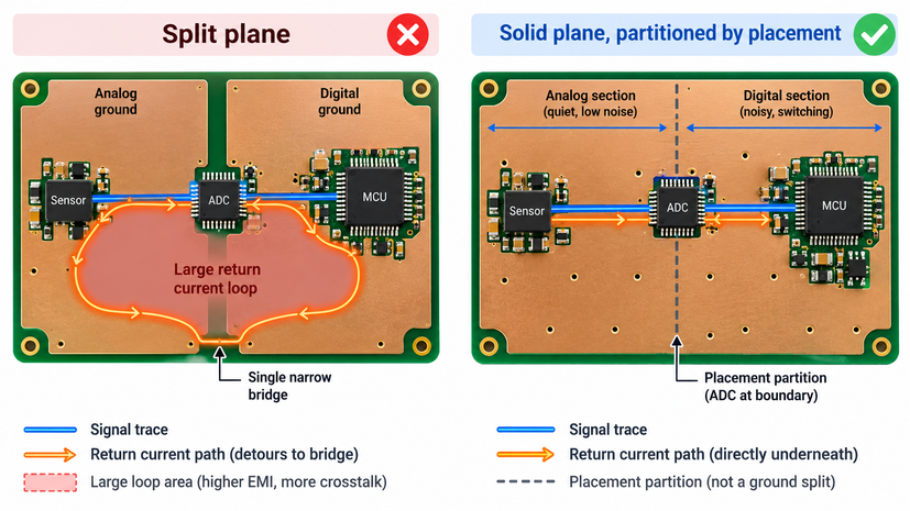
Figure 2: Single-point star grounding compared with multi-point grounding
High-Frequency Current Return Paths in Ground Planes
Return current takes the path of least resistance. The resistance is dominant at low frequencies so that the current flows through the plane. At high frequencies, inductance takes precedence, and the current flow is concentrated beneath the signal trace. Transitions are dependent on board geometry. Based on the current split between the two routes from 500 kHz to 1,000 kHz, return the split in a two-sided board simulation published in In Compliance Magazine. Most of it was under the trace from 10 MHz onward.
This behavior results in two PCB return path layout practices:
- Under fast signals, the plane is to be kept continuous; a slot or split under a trace will cause the return current to go around the gap, thereby enlarging the loop.
- Use a small trace-to-plane height: a smaller height reduces the return current and loop inductance.
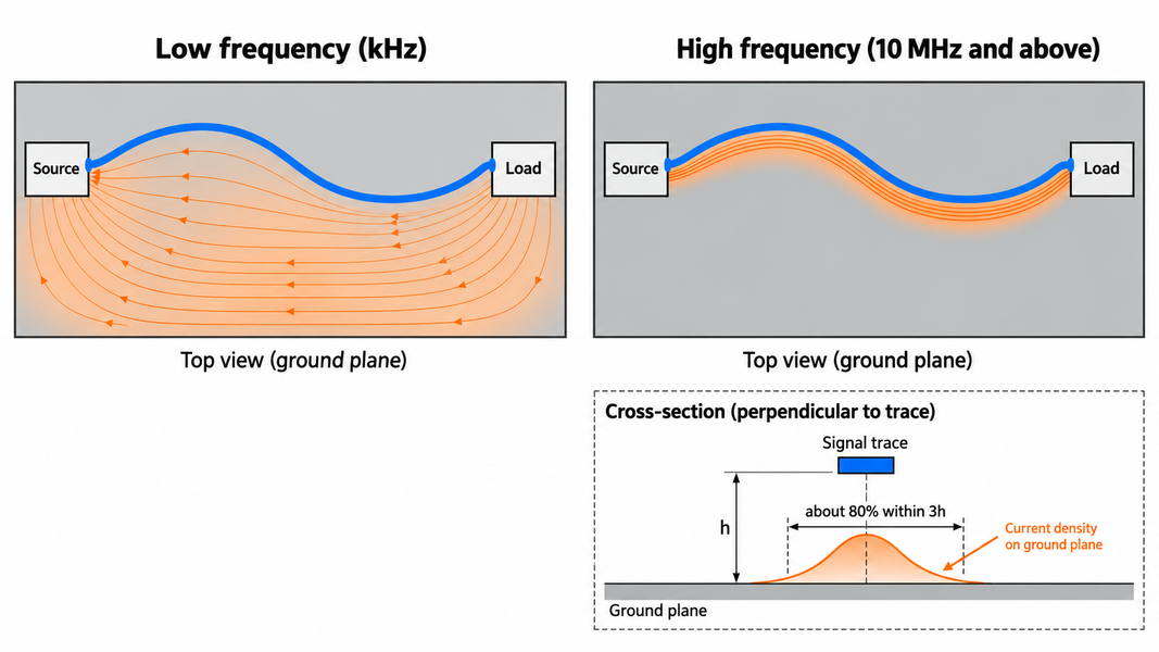
Figure 3: Return current spreading across a PCB ground plane at low frequency and concentrating under the trace at high frequency.
Common Problems Caused by PCB Ground Loops
There are three major issues associated with PCB ground loops: radiated and conducted emission, erroneous analog measurements due to offset, and signal distortion. Ground bounce is similar but is caused by "common" return inductance and not a closed loop.
| Symptom | Likely Mechanism | First Check |
|---|---|---|
| Hum at 50 Hz or 60 Hz and its harmonics | Loop through two mains-earthed connections | Power the board or the instrument from a battery and observe whether the hum disappears |
| ADC reading shifts when a motor or heater turns on | Load return current flows through the copper shared with the analog ground | Measure the voltage between the ADC ground pin and the load return point |
| Emission peaks at clock harmonics in an EMC scan | Large signal loop, or common-mode current on a cable | Look for traces crossing plane gaps and for cables leaving the board |
| Glitches when many outputs switch together | Ground bounce in the package and via inductance | Probe an output held low, using a short ground spring on the probe |
EMI and Radiated Noise from Ground Loop Currents
A current loop is equivalent to a small loop antenna. The differential-mode emission is proportional to the current amplitude, loop area, and the square of the frequency; hence, a large return loop with sharp edges is a strong emitter.
Cables further increase the risk. Common-mode current flows along the cable connecting the boards when the boards' ground potentials differ, causing the cable to act as an antenna. A relatively small amount of common-mode current will suffice. In Compliance Magazine (December 2000), it is found that approximately 8 µA on a 1 m cable at 30 MHz will yield 100 µV/m (FCC Class B) at 3 m.
Signal Distortion and Analog Reference Offset
If a high-current return uses the same copper as the analog ground, the voltage drop across the copper is added to the measured signal. The analog circuit then reads the offset that is after the load current.
| Worked Example | Value |
|---|---|
| Copper | 1 oz (35 µm nominal), about 0.49 mΩ per square at 20 °C |
| Shared path | 40 squares, for example, 2 mm wide and 80 mm long |
| Shared resistance | About 20 mΩ |
| Load return current | 0.5 A |
| Voltage drop in the shared path | About 10 mV |
| 12-bit ADC step at a 3.3 V reference | About 0.81 mV |
| Resulting measurement error | About 12 LSB |
The error is proportional to the load current. When a PWM-controlled motor or heater is used, the sensor reading will show a ripple, and a step load will show a step error.
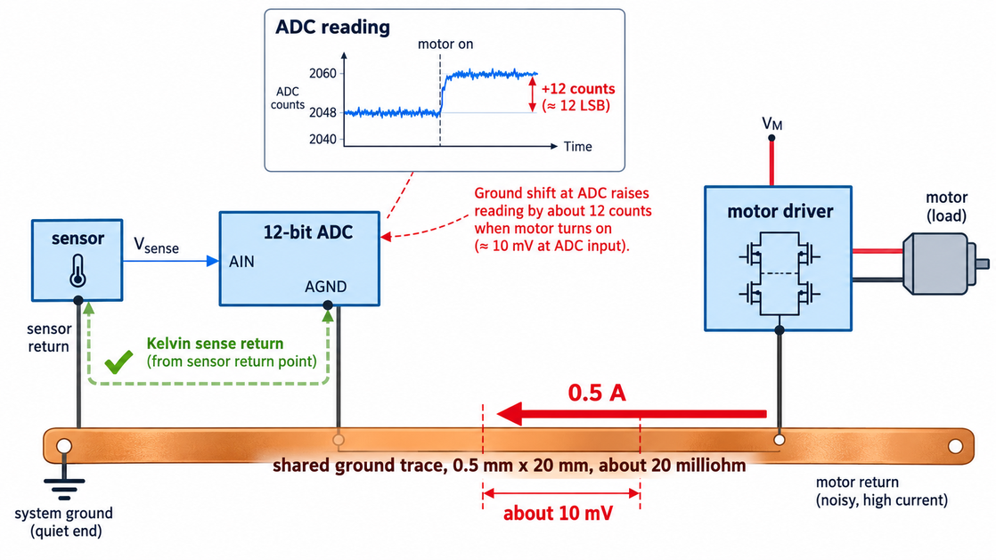
Figure 4: Motor return current flowing through the shared PCB ground copper and shifting the reference of an ADC input.
Ground Bounce and Power Integrity Degradation
Ground bounce is a transient change of an IC's internal ground with respect to the board ground. A closed ground loop does not generate it; rather, it is caused by a return current that rapidly changes in the package and bond wire due to inductance. The common denominator of ground bounce and a conductive ground loop is the return current running through an impedance that another circuit is using as a reference. The corrective actions vary:
- Ground bounce: Minimize common inductance by using multiple ground pins and vias, place capacitors as close as possible to the power pins, and use slower edge rates if timing permits.
- Ground loop: Remove the second return path, minimize common impedance, or isolate the interface.
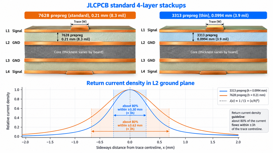
Figure 5: Ground bounce caused by simultaneous switching current through the IC package
How to Prevent Ground Loops: Practical PCB Design Strategies
To avoid ground loops, provide a short, low-impedance path for each return current, one that is not shared with any sensitive circuit. Then, if there are any out-of-the-way cycles the layout cannot avoid, break them.
When to Split Ground Planes and Use Star Grounding
A splitter ground can help reduce coupling between circuits, provided there are no fast signal traces across the splitter. A split is designed to prevent the trace's return current from detouring around the gap, thereby creating a large loop. A single continuous ground plane with a divided-board design is better for most mixed-signal boards than split planes. Separate analog components into one area and digital components into another, and route signals only within their respective areas. Return currents then remain in their area without a physical cut.
In these situations, it's best to use a separate ground or a star point:
- A single data converter with a low digital current: Analog Devices tutorial MT-031 is a split between the analog and digital planes connected at a single point on the converter, with the analog and digital ground pins (AGND and DGND) tied to the analog plane.
- High-current or low-frequency returns: Motor, heater, and LED returns are allowed to return to the supply individually as Cu and reconnect to signal ground at a single star point near the power entry.
- Safety isolation boundaries: The isolated portion should have copper clearances on all layers. The required distance is dependent on the material group, type of insulation, pollution level, working voltage, altitude, and Safety standard.
Using Differential Signaling and Galvanic Isolation
Differential signaling allows for a ground offset between two boards, and galvanic isolation eliminates the conductive path between two grounds. Both neutralize a loop that can only be eliminated by the layout, e.g., a cable-and-mains earth loop.
A differential receiver responds to the difference in voltage between the two inputs and ignores the common-mode voltage. That rejection is only valid within the receiver's common-mode range; for TIA/EIA-485-defined receivers, the common-mode range is -7V to +12V.
| Method | How It Handles a Ground Offset | Example | Main Limitation |
|---|---|---|---|
| Differential signaling | Rejects common-mode voltage within the receiver range | RS-485 transceiver, −7 V to +12 V common-mode range | Offset beyond the range causes errors or damage |
| Optical isolation | No conductive path; light crosses the barrier | 6N137 optocoupler, 10 MBd typical | The LED output can decrease over operating life |
| Magnetic isolation | No conductive path; on-chip transformer coupling | ADuM1201, up to 25 Mbps in the C grade | Each side needs a supply referenced to its own ground |
The JLCPCB Parts library includes a range of isolators, optocouplers, and RS-485 transceivers. On the differential side, use these differential-pair routing practices.
Placing Ground Vias and Decoupling Capacitors for Short Return Paths
At each IC and each layer change, there is a ground via and a decoupling capacitor that sets the length of the high-frequency return loop. By placing these near the current they serve, they maintain that loop small.
- Ground via at each ground pad: Connect each ground pad to the plane through its own short via, rather than sharing one via through a trace.
- Ground via beside each layer change: Place a ground via immediately next to a signal via that moves between two ground-referenced layers.
- Stitching capacitor for a change of reference net: When a signal moves from a ground-referenced layer to a power-referenced layer, place a stitching capacitor between the two planes next to the via to carry the return current.
- Decoupling capacitor at the power pin: Place each high-frequency decoupling capacitor as close to its power pin as the layout allows, with its vias at or beside the pads.
- Stitching vias along plane edges: Keep via spacing a small fraction of the wavelength at the highest frequency of concern. The JLCPCB return-path guide sets a one-tenth-of-a-wavelength upper limit.
The decoupling loop runs from the power pin, through the capacitor and vias to the plane, and then back to the ground pin. At high frequencies, the length of the trace between a pad and its via creates inductance in the loop, and diminishes the effect of the capacitor.
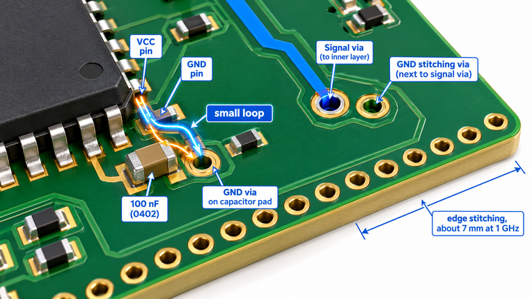
Figure 6: Decoupling capacitor placement showing a short via mounting loop compared with a long trace-connected loop.
PCB Manufacturing Controls That Keep Ground Impedance Low
Return current flows per layout. Fabrication sets the copper thickness, dielectric height, and layer alignment that determine the impedance of that path; therefore, if these are specified at the time of order, they will be built into the board as designed.
Multilayer Stackup Control for Low Ground Impedance
Both the trace impedance and the return current spread are functions of the dielectric height between a signal layer and its ground plane. The thinner the prepreg, the closer the return current to the trace, which reduces the loop inductance.
Every signal layer in a 4-layer stackup with a ground plane on the 2nd layer has an adjacent reference plane. JLCPCB lists its impedance stackups and claims it will only manufacture boards based on the impedance stackup specified by the customer.
| JLCPCB 4-Layer Stackup | L1 to L2 Prepreg | Dielectric Height h | Width Holding About 80% of Return Current (±3h) |
|---|---|---|---|
| JLC04161H-7628 | 7628 × 1 | 0.2104 mm | ±0.63 mm |
| JLC04161H-2116 | 2116 × 1 | 0.1164 mm | ±0.35 mm |
| JLC04161H-3313 | 3313 × 1 | 0.0994 mm | ±0.30 mm |
| JLC04161H-1080 | 1080 × 1 | 0.0764 mm | ±0.23 mm |
Copper Weight, Etching, and Layer Registration
The copper's weight determines the resistance of a ground plane and is most important for high-current, low-frequency returns. The wider the minimum trace and space, the more copper will be removed sideways by the etching process, resulting in less voltage drop with the heavier copper.
| Finished Copper | Nominal Thickness | Sheet Resistance at 20 °C | JLCPCB Minimum Trace/Space |
|---|---|---|---|
| 0.5 oz (inner-layer default) | 17.5 µm | About 0.98 mΩ/sq | Not listed separately |
| 1 oz | 35 µm | About 0.49 mΩ/sq | 0.10/0.10 mm on 2-layer, 0.09/0.09 mm on multilayer |
| 2 oz | 70 µm | About 0.25 mΩ/sq | 0.16/0.16 mm on 2-layer, 0.15/0.15 mm on multilayer |
| 3.5 oz | About 122 µm | About 0.14 mΩ/sq | 0.25/0.25 mm, 2-layer only |
| 4.5 oz | About 157 µm | About 0.11 mΩ/sq | 0.30/0.30 mm, 2-layer only |
Impedance Testing and Electrical Testing: What Fabrication Can Verify
The board is fabricated, and fabrication test results are consistent with design data. They test for impedance and connectivity, but cannot detect a ground loop, which is a property of the design and system wiring.
- TDR impedance test: Time-domain reflectometry (TDR) is a method of measuring the characteristic impedance of test coupons. JLCPCB checks every controlled layer on coupons along the edge of the panel and offers a report with the order.
- Electrical test: Flying probes on prototypes and fixtures in production, test for continuity and isolation on each net. This will detect fabrication opens and shorts, but not connections that are part of the design.
- Inner-layer AOI: A camera compares each etched core with the CAM data before lamination to verify that there are no opens, shorts, or nicks in the plane copper.
FAQs About PCB Ground Loops
Q: Can a Ground Loop Exist on a Single PCB?
Yes. One board can form a ground loop when two return paths join at different potentials, such as a power return trace running parallel to a plane connection.
Q: Does a Solid Ground Plane Eliminate Ground Loops?
No. A solid ground plane prevents most on-board loops by keeping return current under each trace, but it cannot remove off-board loops, such as two mains-earthed instruments or a cable shield grounded at both ends.
Q: How Can I Confirm That Noise Comes from a Ground Loop?
Remove one ground connection at a time. If the hum disappears when an instrument runs on a battery or an earthed cable is unplugged, the loop runs through that connection.
Q: Should AGND and DGND Be Connected Through a Ferrite Bead?
Usually not at a data converter. A ferrite bead introduces impedance between AGND and DGND, so the return current crossing it creates a noise voltage. Analog Devices MT-031 ties both pins to the analog ground plane.
Q: Should Circuit Ground Be Connected to Chassis Ground?
Yes, in many products, at one point near the I/O connectors, either directly or through a capacitor. Cable common-mode current returns to the chassis before reaching the circuit. Safety and EMC requirements set the method.
Conclusion
A PCB ground loop occurs when return current flows through copper used as a reference for another circuit, or when a loop is large enough to radiate and pick up noise. This creates mains hum, analog offset errors, and radiated emission.
To avoid it, use only one solid ground plane for fast signals, separate analog and digital components by location, and minimize vias and decoupling loops. If a loop is closed off the board with cables and mains earth, then use differential signaling or galvanic isolation. After completing the layout, you can request an instant quote for your PCB.
Popular Articles
Keep Learning
How to Choose and Place Decoupling Capacitors for PCB Design
Every digital PCB depends on decoupling capacitors, yet a surprising number of boards still suffer from voltage dips, glitches, and electromagnetic interference (EMI) issues caused by one simple mistake: incorrect placement or selection. This guide walks through what decoupling capacitors do, how to choose the right value, where to place them, and which layout mistakes to avoid, so your next board runs clean on the first try. Key Takeaways Place one decoupling capacitor near each IC's power pin. Use 1......
Effective Solutions to Reduce PCB Ground Loop Noise
Key Takeaways Cause: Multiple ground paths with voltage differences cause hum, ADC errors, and EMI. Strategy: Use star grounding for <1 MHz; use solid ground planes for >10 MHz. Routing: Never route fast traces across split planes to avoid large return loops. Mitigation: Use isolation, differential pairs, and place GND vias/caps close to IC pins. Stackup: Use thinner prepreg to lower return loop inductance. A ground loop occurs when multiple grounds form a closed conductive path, allowing unwanted ele......
Building Effective ESD Protection Into PCB Design
Key Takeaways Layout Rules: ESD spikes rise in nanoseconds; routing layout matters more than part specs alone. Clamp First: Place TVS diodes right at the connector using direct, flow-through traces. Low-Inductance Ground: Use short, wide traces with immediate ground vias to prevent voltage shifts. Capacitance Limits: Use low-capacitance clamps (< 0.5 pF) on high-speed lines like USB 3.x. DFM-Ready: Account for standard via and trace tolerances to ensure reliable board fabrication. ESD protection on a ......
Managing Skin Effect Loss in High-Frequency PCB Design
Key Takeaways Skin Depth Shrinks: High frequencies force current to the trace surface, shrinking depth to 0.66 µm at 10 GHz. Roughness Adds Loss: Copper foil roughness lengthens current paths, sharply increasing high-speed resistance. Plating Affects Signals: Low-conductive finishes like ENIG nickel increase attenuation on exposed lines. Wider Traces Help: Wider traces and thicker dielectrics lower conductor loss by expanding current surface area. Use Smooth Foils: Pairing low-profile copper foils (VL......
How Impedance Controlled Routing Delivers Reliable High-Speed PCB Performance
Key Takeaways Impedance Controlled Routing is essential for reliable high-speed PCB performance above 1 Gbps, eliminating reflections, ringing, and bit errors by precisely targeting interface-specific impedances (USB 90 Ω, PCIe 85 Ω, DDR4 40/80 Ω, HDMI 100 Ω) through field-solver calculations, symmetrical stackups with continuous reference planes, stable low-loss dielectrics, and strict single-ended/differential routing rules. Manufacturing precision in etching, copper profile, and lamination, verifie......
Getting PCB Characteristic Impedance Right for Reliable Signals
Key Takeaways Impedance Defined: Characteristic impedance is set by trace geometry and the reference plane, not by copper DC resistance. Core Factors: Trace width, copper thickness, dielectric height, and dielectric constant determine the impedance value. Reference Plane: High speed traces need a continuous reference plane to prevent signal reflection. Factory Verification: Fabricators adjust trace width and check impedance using time domain reflectometry on test coupons. Design Approach: Select a sta......