How to Choose and Place Decoupling Capacitors for PCB Design
13 min
- What Is a Decoupling Capacitor?
- Why Do Integrated Circuits Need Decoupling Capacitors?
- How Does a Decoupling Capacitor Work?
- Decoupling Capacitor vs. Bypass Capacitor
- How to Choose the Right Decoupling Capacitor
- Why is 100 nF the Most Common Decoupling Capacitor Value?
- How to Place Decoupling Capacitors Correctly
- Decoupling Capacitor Layout Recommendations for Different PCB Types
- Bulk Capacitor vs. Local Decoupling Capacitor
- Common Decoupling Capacitor Mistakes to Avoid
- Typical Decoupling Capacitor Configurations for Popular MCUs
- Decoupling Capacitor Design Checklist
- Conclusion
- FAQs about Decoupling Capacitors
Every digital PCB depends on decoupling capacitors, yet a surprising number of boards still suffer from voltage dips, glitches, and electromagnetic interference (EMI) issues caused by one simple mistake: incorrect placement or selection.
This guide walks through what decoupling capacitors do, how to choose the right value, where to place them, and which layout mistakes to avoid, so your next board runs clean on the first try.
Key Takeaways
- Place one decoupling capacitor near each IC's power pin.
- Use 100 nF X7R Multi-Layer Ceramic Capacitors (MLCCs) for most digital circuits.
- Pair local decoupling with a bulk capacitor near the power supply.
- Keep current loops and trace lengths as short as possible.
- Always follow the specific IC datasheet guidelines.
What Is a Decoupling Capacitor?
A decoupling capacitor is a small capacitor placed directly across an integrated circuit's (IC) power and ground pins. It acts as a local energy reservoir, supplying instantaneous current during switching events and filtering high-frequency noise from the power rail. In the PCB industry, it is often abbreviated as "decap."
A decoupling capacitor provides a nearby source of charge whenever an Integrated Circuit experiences a sudden current demand. By supplying this transient current locally, it helps maintain a stable supply voltage. Its primary functions are to:
- Supply instantaneous current during high-frequency switching events.
- Reduce voltage droop on the power rail.
- Filter high-frequency switching noise.
- Improve overall power integrity across the Power Distribution Network (PDN).
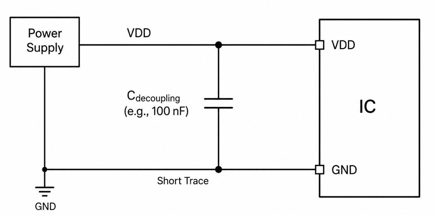
Figure: Decoupling capacitor connected in parallel across an IC's power and ground pins.
Note
Understanding the capacitor symbol during schematic design helps ensure the correct components are selected, preventing assembly issues such as polarity errors with polarized capacitors.
Why Do Integrated Circuits Need Decoupling Capacitors?
Digital ICs switch internal transistors millions or billions of times per second. Each switching transient causes a sudden current demand. Because every trace and via on a board has parasitic resistance and inductance, this sudden demand creates a brief voltage drop on the supply rail.
Without proper decoupling, a PCB may experience:
- Voltage droop and ground bounce.
- Signal integrity problems (jitter, ringing, crosstalk).
- Increased EMI radiating from power traces acting as antennas.
- Random microcontroller resets or unpredictable logic errors.
A decoupling capacitor absorbs this transient demand before it reaches the rest of the board, keeping the electrical disturbance local instead of system-wide.
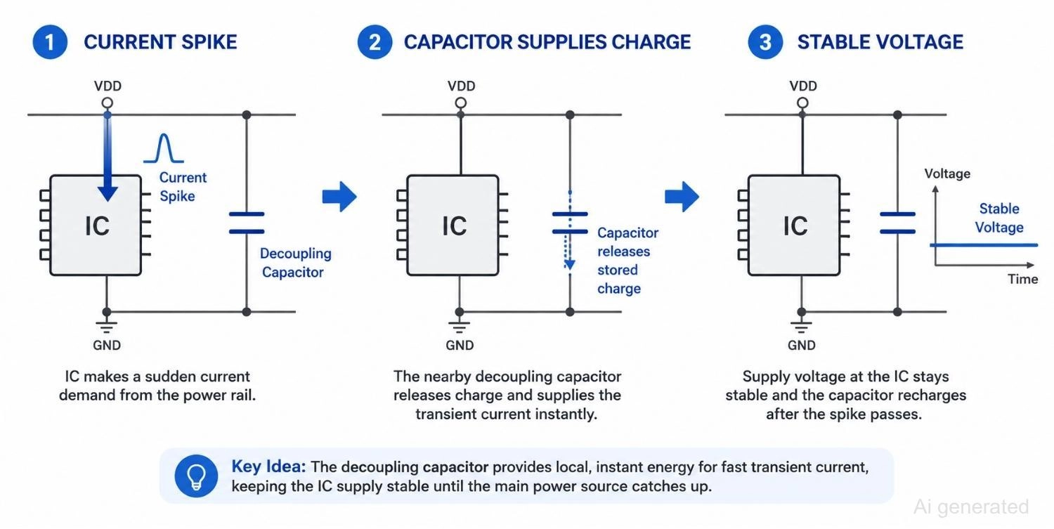
Figure: Showing a current spike, a decoupling capacitor supplying charge, and the resulting stable voltage.
How Does a Decoupling Capacitor Work?
During switching, the IC briefly draws current from the nearby capacitor instead of the main power supply. Once the transient passes, the capacitor recharges from the supply rail. Because the capacitor sits physically close to the IC, it responds far faster than the longer return current path back to the voltage regulator.
Decoupling Capacitor vs. Bypass Capacitor
The terms decoupling capacitor and bypass capacitor are often used interchangeably, and in most practical designs, a single MLCC performs both jobs. However, they serve slightly different theoretical roles.
| Feature | Decoupling Capacitor | Bypass Capacitor |
|---|---|---|
| Primary Purpose | Local energy storage for transient current. | Diverts high-frequency noise/AC signals to ground. |
| Location | Extremely close to the individual IC's power pins. | Near the main supply input, connector, or noise source. |
| Frequency Focus | Broad, including mid-to-high frequency transients. | Primarily high frequency. |
| Typical Component | MLCC (ceramic). | MLCC (ceramic) or electrolytic. |
In modern digital design, one 100 nF ceramic capacitor at each IC power pin usually covers both roles. For a deeper breakdown of when the routing and layout distinctions actually matter, you can refer to the definitive guide to bypass capacitors in PCB layout.
How to Choose the Right Decoupling Capacitor
Selecting a decoupling capacitor comes down to five parameters: value, dielectric, voltage rating, package size, and self-resonant frequency.
Capacitance Value
- 100 nF (0.1 uF): Standard local decoupling value for most digital logic ICs, microcontrollers, and logic gates.
- 1 uF: Mid-frequency support, often paired alongside 100 nF on noise-sensitive or mixed-signal supply rails.
- 10 uF and above: Bulk capacitor for slower, larger current transients across a whole rail or board segment.
Dielectric Type
- X7R: Stable across temperature (minus 55 to plus 125 degrees Celsius), the standard choice for general digital decoupling.
- X5R: Similar to X7R with a narrower temperature range (minus 55 to plus 85 degrees Celsius), common in compact consumer electronics.
- C0G/NP0: Highly stable and precise, but low capacitance per package size. Typically reserved for analog filters or RF circuits rather than power supply decoupling.
Voltage Rating
Always select a voltage rating with headroom above the rail voltage. Ceramic capacitors lose effective capacitance as DC bias approaches their rated voltage (known as DC bias aging), sometimes by 60 to 80 percent. A 10 V or 16 V rated capacitor on a 3.3 V or 5 V rail keeps actual capacitance close to the labeled value.
Package Size
- 0402: Compact, used in dense high-speed PCB designs; slightly higher cost and harder to hand-solder.
- 0603: Common balance of size and cost for most digital boards.
- 0805: Easier to hand-assemble or rework, used where board space is generous.
While through-hole capacitors were once common, modern designs favor surface-mount devices due to their vastly superior high-frequency performance and minimized parasitics. You can read more about this in our comparison of surface-mount technology vs through hole.
Self-Resonant Frequency (SRF)
Every real capacitor has parasitic inductance from its leads, internal structure, and mounting traces (Equivalent Series Inductance, or ESL).
Below its self-resonant frequency, the capacitor behaves capacitively, and impedance falls as frequency rises. Above the SRF, that parasitic inductance dominates and impedance rises again, so the capacitor stops decoupling effectively. Smaller capacitance values and smaller packages generally have lower ESL and therefore a higher SRF.
This is the core reason designs combine multiple capacitor values: a 100 nF capacitor remains effective at higher frequencies where a typical 10 uF capacitor has already passed its self-resonant frequency, and the 10 uF capacitor covers lower frequencies the 100 nF cannot supply.
Even a capacitor with an ideal SRF performs poorly if decoupling capacitor placement puts it too far from the IC, so component selection and PCB placement always work together.
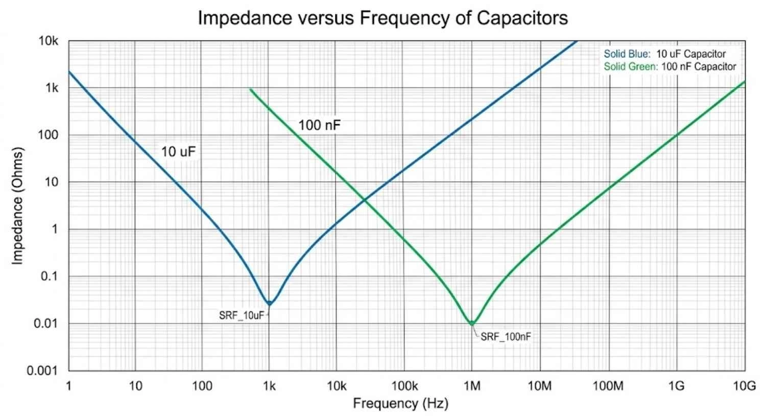
Figure: Impedance versus frequency chart comparing a 10 microfarad capacitor and a 100 nanofarad capacitor, showing each capacitor's self-resonant frequency dip.
| Purpose | Typical Value | Capacitor Type |
|---|---|---|
| High-frequency local decoupling | 100 nF | X7R MLCC |
| Mid-frequency support | 1 uF | X7R MLCC |
| Bulk / board-level decoupling | 10 to 47 uF | Ceramic or tantalum |
Note
Always check the IC's datasheet first. Manufacturer-recommended values and layout placement guidelines override generic rules of thumb.
A decoupling capacitor is one part of the PCB's Power Distribution Network (PDN), whose overall goal is to maintain a stable, low-impedance supply rail across a wide frequency range, from DC up through the switching transients generated by high-speed digital logic.
Why is 100 nF the Most Common Decoupling Capacitor Value?
100 nF became the industry standard because it:
- Provides good high-frequency performance in a small package.
- Fits easily into compact MLCC packages with low parasitic inductance.
- Is highly inexpensive and widely available across every footprint.
- Works well as a general-purpose value for most digital ICs.
However, high-speed processors, FPGAs, and System-on-Chips (SoCs) often require additional 1 uF and bulk capacitors to cover the lower-frequency transients a single 100 nF capacitor cannot supply. For this reason, 100 nF remains the default starting point for digital decoupling, with additional capacitance added only when required by the application's power demands.

You can easily find and source recommended MLCCs directly from the JLCPCB Parts Library.
How to Place Decoupling Capacitors Correctly
Proper placement of decoupling capacitors is just as important as selecting the correct capacitance value. Placement determines whether a correctly sized capacitor actually works.
Place Close to IC Power Pins
Keep the capacitor within a few millimeters of the IC's power pin. Distance adds trace inductance, and inductance is exactly what defeats high-frequency decoupling.
Keep Traces Short
Short, direct traces from the capacitor to the power and ground pins minimize parasitic resistance and inductance along the current path.
Minimize Current Loop Area
The loop formed by the power pin, the capacitor, and the ground connection should be as small as physically possible. A smaller loop radiates less EMI and presents lower inductance. Poor decoupling capacitor placement increases loop inductance and reduces high-frequency effectiveness.
Connect Directly to the Ground Plane
Route the capacitor's ground pad straight down to the ground plane with the shortest possible return current path. Avoid routing the ground connection through several layers or long traces.
Use Dedicated Vias
When a via is required between the capacitor pad and the plane, use a dedicated via placed as close to the pad as possible, and use multiple vias in parallel where space allows to reduce inductance further.
One Capacitor per Power Pin?
Many modern ICs, especially FPGAs and high-pin-count microcontrollers, have multiple power (VDD) pins. As a general rule, place one local decoupling capacitor per power pin unless the datasheet explicitly states that pins share an internal plane.
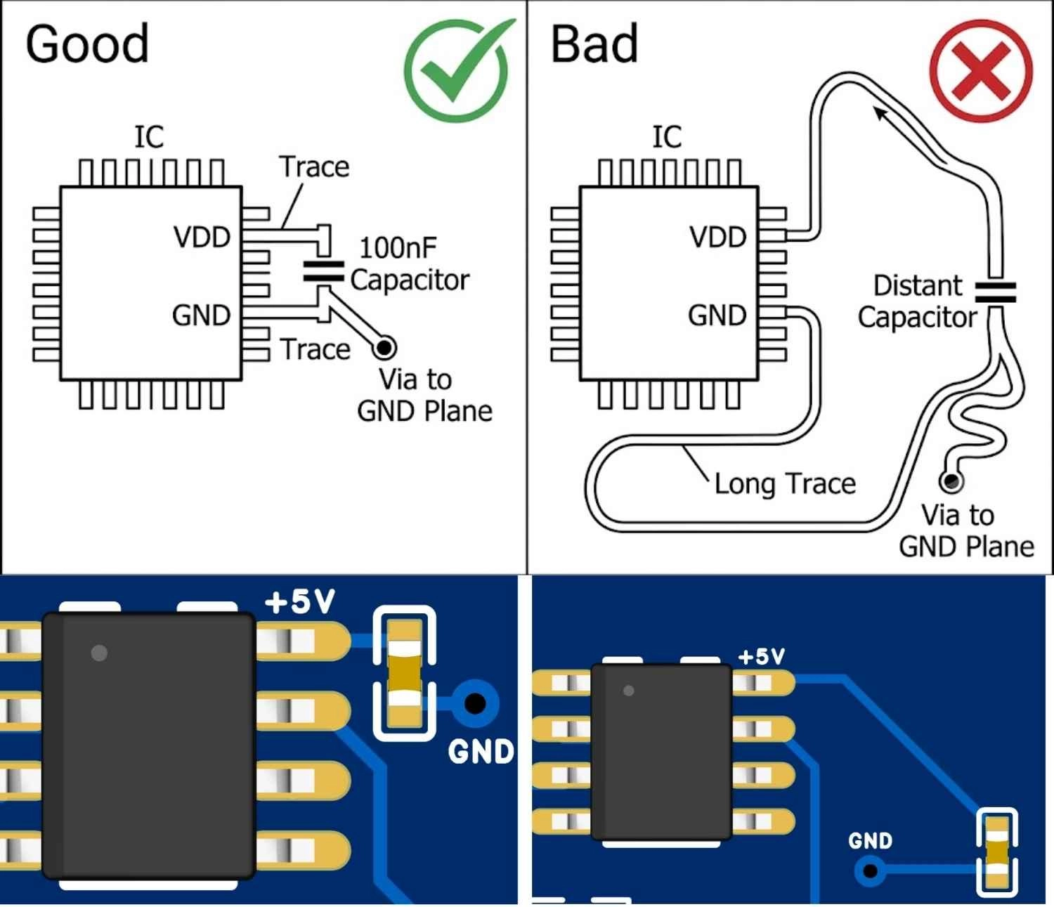
Figure: PCB layout comparison of correct close placement versus incorrect distant placement of a decoupling capacitor.
Decoupling Capacitor Layout Recommendations for Different PCB Types
| PCB Design Scenario | Recommended Decoupling Capacitor Placement |
|---|---|
| Two-layer Board | Place the capacitor as close as physically possible to the IC pin, since there is no dedicated internal ground plane to fall back on. |
| Four-layer Board | Use a solid ground plane directly beneath the capacitor and IC layer for short, low-inductance return paths. |
| High-speed PCB | Use multiple MLCCs of different values (e.g., 10 nF, 100 nF) in parallel to cover a wider frequency range. |
| FPGA / MCU Boards | Consider via-in-pad construction where the via sits inside the capacitor pad itself, minimizing trace inductance. |
Bulk Capacitor vs. Local Decoupling Capacitor
A complete power distribution network needs both capacitor types working together, not one in place of the other:
- Bulk capacitor: Supports slow, high-energy current changes across an entire supply rail, typically 10 to 47 uF or higher near the power input or regulator output.
- Local decoupling capacitor: Handles fast-switching transients at each IC; typically 100 nF, sometimes with an added 1 uF.
- Together: They provide low impedance across a broad frequency range, from low-frequency rail changes up through fast digital switching events.
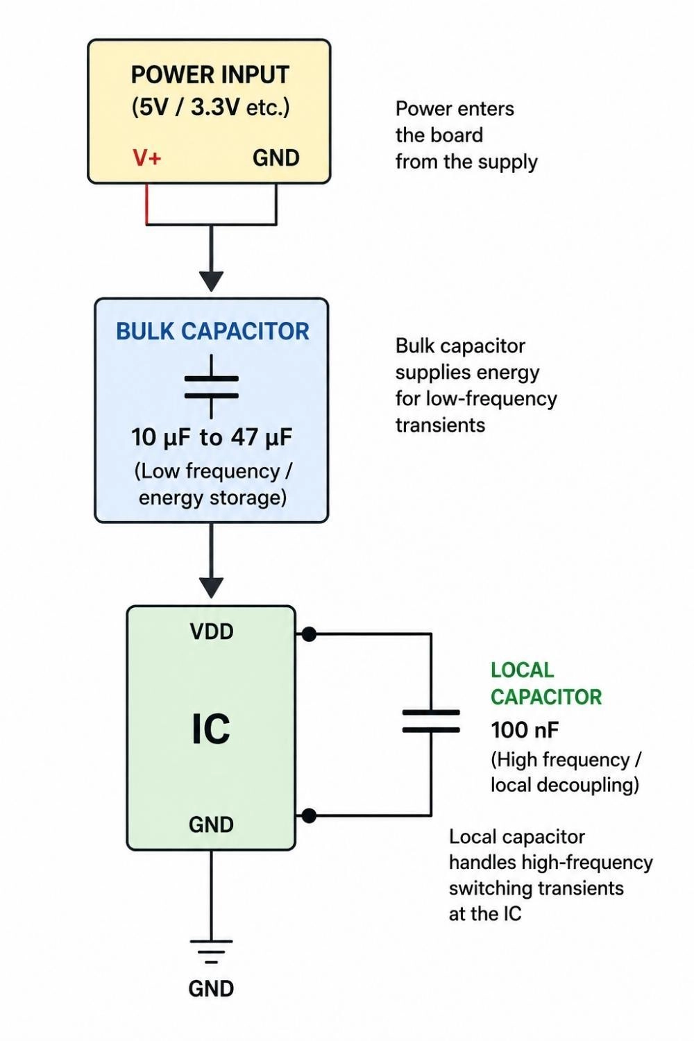
Figure: Power flow diagram from input through a bulk capacitor to an IC with a local 100 nF decoupling capacitor.
Common Decoupling Capacitor Mistakes to Avoid
| Mistake | Engineering Impact |
|---|---|
| Capacitor placed far from the IC | Added trace inductance defeats high-frequency filtering. |
| Long, thin traces to the capacitor | Increases resistance and inductance in the transient current path. |
| One capacitor shared across many ICs | Each IC needs its own local reservoir for fast, independent transients. |
| Wrong dielectric choice (e.g., Y5V) | Capacitance drops sharply with temperature shifts and DC bias. |
| Ignoring the ground plane connection | Long ground return current paths increase loop inductance and EMI. |
| Relying only on electrolytic capacitors | High Equivalent Series Resistance (ESR) and poor high-frequency response compared to ceramic MLCCs. |
| Wrong package size for the layout | Either wastes board space or limits how close it can sit to the pin. |
| Ignoring the self-resonant frequency | A capacitor's SRF limits how high in frequency it remains effective. |
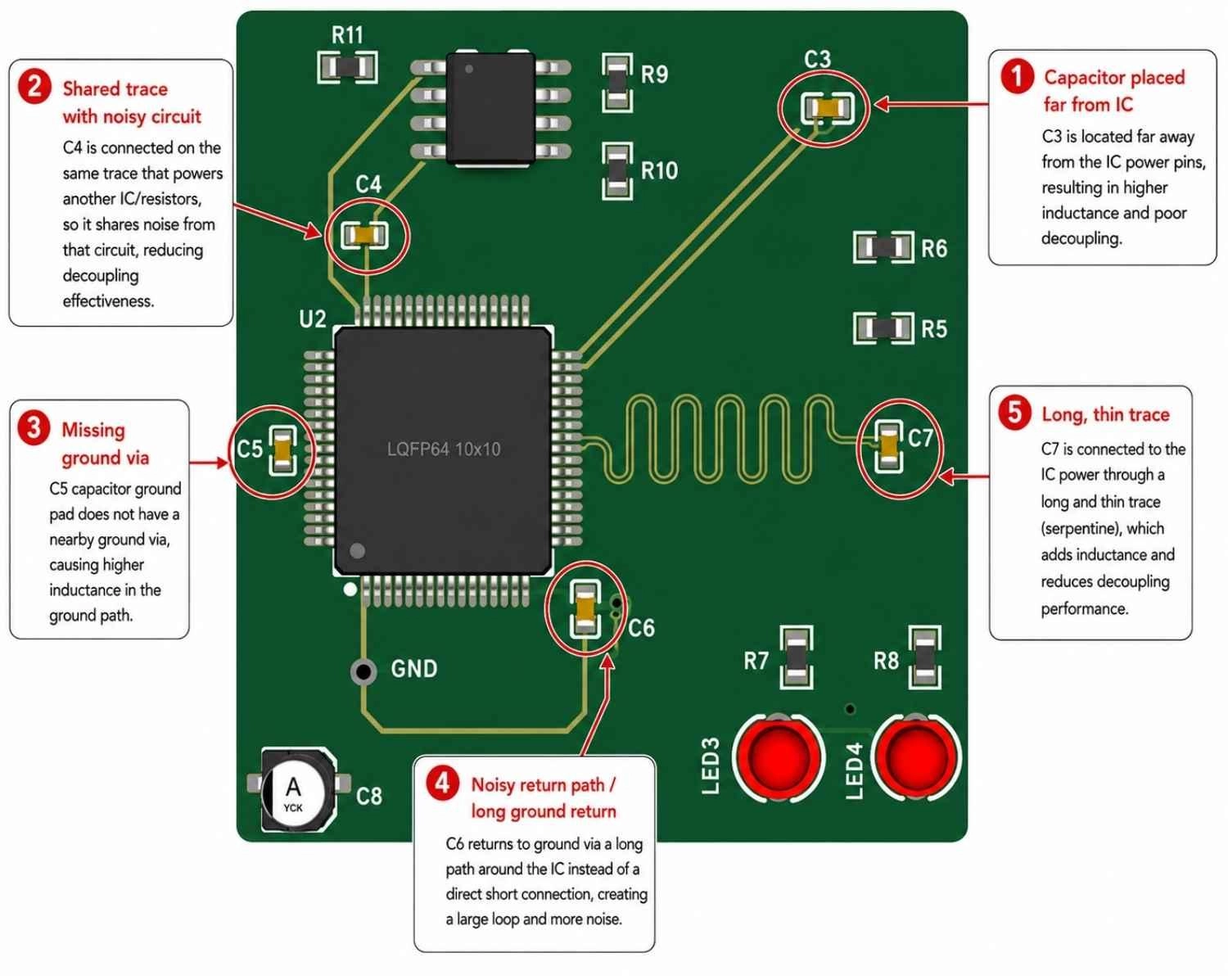
Figure: PCB layout highlighting common decoupling capacitor placement mistakes.
Typical Decoupling Capacitor Configurations for Popular MCUs
Most MCU manufacturers recommend placing a local ceramic decoupling capacitor adjacent to every supply pin, with exact values specified in the device hardware design guidelines.
| Device | Typical Decoupling Setup |
|---|---|
| STM32 Microcontrollers | 100 nF ceramic on every VDD pin, plus a 4.7 uF bulk capacitor near the supply pin, per ST's hardware design guide. |
| ESP32 | 100 nF close to the chip's power pins, plus a 10 uF capacitor near the regulator output, per Espressif's hardware design guidelines. |
| ATmega328 | 100 nF on VCC, plus a 10 uF bulk capacitor near the board's power input. |
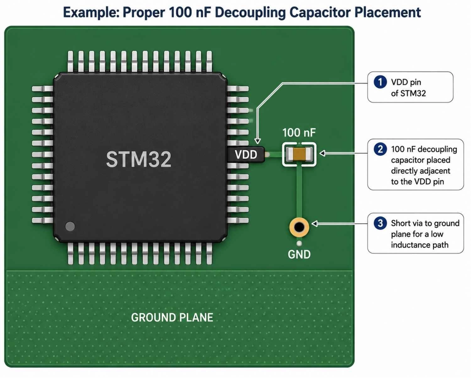
Figure: Example PCB layout showing a 100 nF decoupling capacitor placed next to an STM32 VDD pin with a short via to the ground plane.
Decoupling Capacitor Design Checklist
- Place the capacitor within a few millimeters of the power pin.
- Keep power and ground traces as short and wide as possible.
- Connect directly to a solid ground plane to minimize the return current path loop.
- Use X7R or X5R MLCCs for general digital decoupling.
- Add a bulk capacitor near the regulator or power entry point.
- Always follow the IC datasheet's recommended values and placement.
Conclusion
Selecting the correct capacitance is only half the job. Low-ESL MLCCs, short PCB traces, solid ground planes, and datasheet-recommended placement work together to create a stable power distribution network. Following these practices improves signal integrity, reduces EMI, and increases the reliability of both simple microcontroller boards and complex high-speed digital systems.
Designing an effective decoupling network is only part of building a reliable PCB. Equally important is ensuring your layout can be manufactured exactly as intended.
-
With advanced PCB fabrication, precision SMT assembly, and millions of readily available components, JLCPCB helps you turn proven designs into production-ready hardware. Once your design is complete, simply upload your design files to get an instant online quote and move from prototype to production with confidence.
FAQs about Decoupling Capacitors
Q: How do you calculate the exact decoupling capacitor value for high-speed ICs?
To calculate the capacitor value, determine the transient current demand, the maximum allowed voltage ripple, and the transient duration. Using the formula: Capacitance = (Transient Current × Transient Duration) ÷ Maximum Allowed Ripple Voltage
You can estimate the minimum local capacitance required before bulk power delivery takes over. However, modeling the entire PDN impedance is the industry-standard approach for high-speed boards.
Q: What happens if you place a decoupling capacitor on the opposite side of the PCB?
Placing the capacitor on the opposite side (e.g., the bottom layer) requires vias to connect it to the IC pin. Vias add parasitic inductance (typically around 1 to 2 nH per via). This added inductance can significantly degrade the capacitor's ability to filter high-frequency switching noise. If you must place capacitors on the bottom side, use multiple vias in parallel to reduce inductance.
Q: Why is a low Equivalent Series Resistance (ESR) critical for decoupling capacitors?
A low Equivalent Series Resistance (ESR) allows the capacitor to discharge its stored energy almost instantly. High Equivalent Series Resistance (ESR) limits the transient current flow, causing the capacitor to respond too slowly to the IC's switching demands, which leads to voltage droops and power rail noise.
Q: How does a solid ground plane influence decoupling capacitor performance?
A solid ground plane provides a low-impedance return current path back to the decoupling capacitor. Without a solid ground plane, return currents must travel through long, inductive traces, which increases the loop area, ruins power integrity, and elevates EMI radiation.
Popular Articles
Keep Learning
Navigating the Impedance Landscape: Selecting the Right Impedance for USB, Ethernet, HDMI, and SD Card Interfaces
Introduction In the realm of high-speed digital communication, choosing the right impedance is a critical aspect of successful PCB design. Impedance matching ensures optimal signal integrity, minimizes reflections, and enhances the overall performance of interfaces such as USB, Ethernet, HDMI, and SD Card. In this blog post, we'll explore the importance of impedance, the factors influencing impedance selection, and best practices for ensuring reliable data transmission in these widely used interfaces.......
A Beginners Guide to Impedance Control in PCBs
When a digital signal is transmitted from one point to another, it causes a change in the state of the signal line. This change can be understood as an electromagnetic wave moving through the circuit. Reflection occurs when this wave encounters a boundary between different mediums. At this boundary, some of the wave's energy continues as a signal, while the rest is reflected. This process repeats until the energy is either absorbed by the circuit or dissipated into the environment. For electrical engi......
What is PCB Signal Attenuation: How Signals Weaken Over Distance and How to Mitigate It
Key Takeaways Primary Causes: Signal attenuation is mainly caused by skin effect (conductor loss) and substrate energy absorption (dielectric loss). How to Mitigate: Reduce loss by using wider traces, low-loss materials, controlled impedance, and removing via stubs. JLCPCB Solutions: JLCPCB offers Rogers high-frequency laminates, High-TG FR4, precision impedance control, and backdrilling to protect signal integrity. As a signal travels from the source to the load through PCB conductors, the signal is ......
Understanding Analog and Digital Ground in PCB Design
When working on printed circuit board (PCB) design, proper grounding is crucial for ensuring signal integrity, minimizing noise, and maintaining reliable performance. Two common types of ground planes used in PCB layouts are Analog and Digital ground. In this article, we will explore the differences between analog and digital ground, their significance in PCB design, and best practices for their implementation. Analog Ground vs. Digital Ground Analog ground and digital ground have separate purposes in......
Design Guide for USB-3.0 Differential Signaling
In the world of data transfer, USB 3.0 is the Usain Bolt to USB 2.0’s friendly jogger. USB 2.0 is called “High Speed” and limped along at 480 Mb/s, whereas USB 3.0 SuperSpeed rockets up to 5 Gb/s (over ten times faster). But this speed jump brings full‑duplex operation and new differential transmit (SSTX) and receive (SSRX) pairs on dedicated pins. USB 2.0 D+/D– lines handle enumeration and legacy data, while two new 5 Gb/s high‑speed differential pairs carry SuperSpeed data in each direction. While m......
Understanding Impedance Matching for High-Speed PCB Designs
With the advancement of technology and the ever wider application of integrated circuits, the frequency and speed of electronic signal transmission have been increasing, making it essential for PCB conductors to provide high-performance transmission lines. These transmission lines are responsible for delivering signals from a source to the input of a receiver accurately and completely. This requirement emphasizes the need for impedance matching. Electrical impedance, commonly represented as Z and meas......