
Mastering Split Planes for Cleaner Power Delivery and Better Signal Integrity
11 min
- The Role of Split Planes in Modern PCB Design
- Benefits and Potential Risks of Split Planes
- Best Practices for Effective Split Plane Design
- Manufacturing Considerations for Split Plane PCBs
- JLCPCB's Expertise in Split Plane Implementation
- FAQ about PCB Split Plane
- Conclusion
Key Takeaways
- Split power planes when needed for multiple voltage domains or analog/digital isolation, but never split ground planes — always keep ground continuous for clean return paths.
- Avoid routing high-speed signals across splits; if unavoidable, use stitching capacitors (0.1 µF) and ensure differential pairs cross together.
- Place split power planes next to a solid ground layer, maintain ~10 mil moat width, and use proper decoupling near IC pins.
- Good split plane design significantly reduces noise and EMI, but poor implementation can worsen signal integrity.
Ever had a new board up and running where analog sensor values kept vibrating, or sound output ends up sounding like it has a hum in it when it shouldn't? In 9 out of 10 cases, it is your power distribution that's at fault. Plus, one of the most misunderstood tools to fix it is the Split Plane. As the name suggests, a Split Plane is a copper plane on your PCB that is subdivided into separate areas. When properly implemented, it separates the noisy digital circuits from analog circuits that are sensitive to noise and tidies up multiple voltage rails.
If misapplied, it ruins your return paths and turns your board into an EMI antenna. Balancing the act of splitting planes is a power integrity and signal integrity game. This guide will explain what split planes are, when they are genuinely an asset, and the precautions you must take and must not take to differentiate a clean layout from a noisy mess.
The Role of Split Planes in Modern PCB Design
What Split Planes Are and When They Are Needed
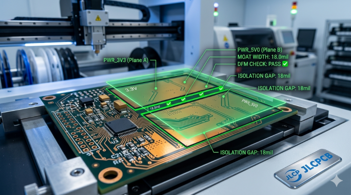
A PCB Split Plane is a one-layer copper board that is etched into one or more electrically isolated areas, referred to as a moat. Different voltages may be applied to each zone, and/or each zone may provide a different functional block. The most valid excuse for splitting a plane is to route two or more separate power rails on a single layer. A split plane is usually required when:
- There are several supply voltages (such as 1.8 V, 3.3 V, and 5 V) on a single power layer.
- The sensitive analog domain needs to be isolated from noisy digital switching currents.
- For a mixed-signal device (ADC or DAC), there are separate analog and digital power pins specified on its datasheet.
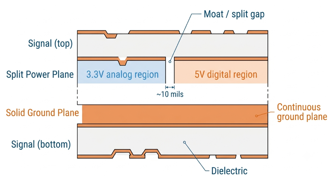
It is a common occurrence that Power Plane Splits are needed. Ground Plane Splits, however, are hazardous, typically not a good idea since a continuous ground provides a clean return path for signals.
Common Use Cases in Power and Ground Distribution
The traditional application is the mixed-signal board. When the analog supply is in its own quiet zone, it is advantageous for an audio codec, a precision data acquisition system, or a medical sensor front-end. You can split the power plane and power that section of the power plane through a ferrite bead or a separate regulator. Other common scenarios are:
Multi-rail power layers: powering an FPGA core at 1.2 V, an I/O layer at 3.3 V, and a peripheral layer at 5 V.
Noise-sensitive instrumentation: where a few millivolts of ripple on a power source will ruin a measurement.
High-frequency designs, which run at frequencies of several hundred megahertz or higher, are where the supply noise directly affects the timing margins.
Benefits and Potential Risks of Split Planes
Improved Noise Isolation and Voltage Domain Management
Domain isolation is the greatest benefit. Switching noise is prevented from leaking from one voltage domain to another via a shared plane impedance by providing each rail with its own copper area. If an analog supply is properly isolated from a digital supply, some mixed-signal designs claim to have a 20 dB noise-coupling reduction. The advantages are pretty nice:
- Less cross-contamination between voltage domains: less voltage contamination seen by each rail from other circuits.
- Lower ground bounce in the areas critical for precision analog.
- Confined EMI: interference remains localized and isn't radiated everywhere.
- Dedicated regions: routing & decoupling are much easier to reason about.
Risks to Return Paths and Signal Integrity
Each high-speed signal creates a return current that would prefer to travel on the plane immediately below the trace. A gap through which the return current cannot flow directly is encountered when a signal crosses a split. The moat then causes the return current to take a longer detour around the moat, thus making the current loop larger. In that loop, you're doing 3 bad things at once.
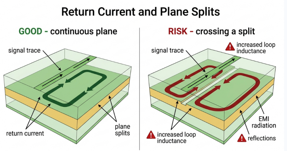
It increases the loop inductance, hence signal integrity is compromised, and there will be reflections at the impedance discontinuity. It turns into a very effective radiator, increasing your EMI figure and endangering your compliance with EN 55032 or FCC part 15. This allows for crosstalk between the signals that share that detour path.
Best Practices for Effective Split Plane Design
Proper Placement, Moating, and Stitching Via Strategies
First, perform the split at the physical split between blocks of function – analog on one side of the moat, digital on the other. The moat itself does not have to be wide; a gap of about 10 mils (0.254 mm) is usually enough to isolate the domains. If the two domains need to be joined, do so with a single controlled bridge, not a leaky boundary. Some techniques that have been proven:
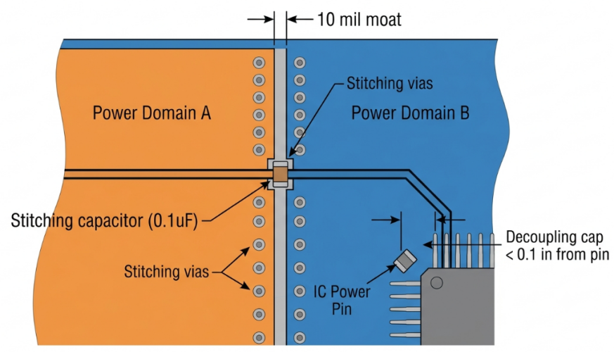
- Stitching vias: connect split power regions to a continuous ground plane on an adjacent layer to keep return currents tightly coupled.
- Stitching capacitors: make sure there is a high-frequency AC return path across which a signal is required to cross by installing a small capacitor, usually 0.1 µF or 1 nF, across the moat.
- Decoupling discipline: Use decoupling capacitors within 0.05 to 0.1 inches (1.3 mm to 2.5 mm) of each IC power pin to keep the local plane impedance in the milliohm range.
Handling Plane Splits with Differential Pairs and High-Speed Signals
High speed and singles/plane, a bad mix. The most basic is to never cross a plane split with your fast signals. If a crossing is unavoidable, follow these guardrails:
- On differential pairs (USB 3.0 at 90 Ω and PCIe and LVDS), both traces of the pair cross the split at the same point, so skew remains matched.
- Add a stitching capacitor next to the crossing to provide a return path for the crossing current.
- Use a pair of continuous ground planes instead of a split power plane as much as possible.
- Layer stack up considerations for optimal performance.
Layer Stackup Considerations for Optimal Performance
How forgiving a split plane will be depends upon your stackup. The basic rule is that whatever layer you split for power should be placed over a solid, continuous ground plane. This will provide a clean return path for each signal, even if the overlying power plane is broken up. Here are a few stackup guidelines to follow:
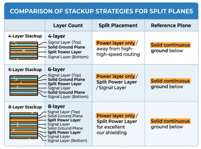
In a 4-layer board, use splits only for the power layer and use one internal layer as a solid ground. For 6-layer and above: Make sure that the high-speed routing layers are sandwiched between solid reference planes, and that any splits are clear away from the high-speed routing layers. Minimize the thickness of the dielectric between the signal layer and the reference plane to make the return current coupling tight and to control the impedance.
Manufacturing Considerations for Split Plane PCBs
Etching Precision and Plane Integrity Control
The moat between domains is totally determined by the etching process. With etching irregularity, it is possible to get a 10 mil gap under-etched (copper bridging two domains) or over-etched (eroding clearances elsewhere). Both of these result in the violation of the isolation you set up. Factors that contribute to the integrity of planes during manufacture are:
- Tight etch tolerance to ensure that the moat width is as per design intent.
- Balancing of copper to avoid warpage at a large plane area split unevenly across the panel.
- Copper edges around the moat should be kept clean, as the copper slivers or debris can cause a short circuit.
Ensuring Reliable Performance During Fabrication
In addition to the etch, the entire fabrication chain has an impact on how a split plane behaves in the field. Lamination registration is the measurement that will tell you if your split power layer is correctly positioned on the ground plane that it relies on. Misregistration is a relationship change between trace, gap, and reference. This is based on some checks to ensure reliable production:
- Layer-to-layer registration has been checked during lamination and drilling.
- Uniformity of plating in stitching vias to maintain a low impedance via-to-plane connection.
- Electrical Testing to verify each isolated Domain is actually isolated, and each connection conducts.
JLCPCB's Expertise in Split Plane Implementation
Advanced DFM Review for Complex Split Plane Layouts
JLCPCB's instant quoting system automatically conducts a Design for Manufacturing (DFM) review on every upload and alerts any problems, such as insufficient clearances or copper slivers around a moa,t before getting into production. For intermediate designers, this early feedback is a safety net that captures plane-integrity issues at an early stage when they can be easily resolved. EasyEDA is directly integrated with JLCPCB, so you can make changes to a split power layer and re-check the manufacturability in the same workflow. Because of the small circle, it is easy to adjust the width of moats and stitching strategies without guesswork.
Precision Manufacturing Ensuring Clean Power Delivery
Accurate copper is the first step in clean power delivery. When you design an isolation, JLCPCB's controlled etching process brings it into reality. The platform spans a variety of different surface finishes (HASL to ENIG), multiple layer counts, and controlled-impedance capabilities, which are essential for split planes. With PCBs starting at $2 and fast turnaround times of 1 to 2 days, you can prototype a split-plane board, measure it, and refine it without having to wait long periods of time. This quick feedback is extremely useful when tuning power and ground distribution.
FAQ about PCB Split Plane
Q: What is a Split Plane in PCB design?
A split plane is a single copper layer divided into two or more electrically isolated regions by an etched gap called a moat. Each region can carry a different voltage rail or serve a different functional block, such as separating analog and digital power domains.
Q:Should I split the ground plane the same way I split a power plane?
Generally, No. Power plane splits are common and often necessary for multiple voltage rails, but ground plane splits break return paths and usually hurt signal integrity. Keep your ground continuous so every signal has a clean path home.
Q: What happens when a high-speed signal crosses a plane split?
The return current is forced to detour around the gap, increasing loop inductance, adding reflections, and raising EMI. If a crossing is unavoidable, place a stitching capacitor right at the crossing and reference the signal to a continuous ground plane.
Q: How wide should the moat between split planes be?
A gap of around 10 mils (0.254 mm) is typically enough to isolate two power domains. The gap behaves as an AC path through plane capacitance and nearby decoupling capacitors, so excessively wide moats provide little extra benefit.
Conclusion
Mastering split planes is one of the most effective ways to achieve cleaner power delivery and superior signal integrity in modern mixed-signal PCB designs. When used correctly, split power planes allow you to isolate sensitive analog circuits from noisy digital domains, minimize crosstalk, reduce ground bounce, and maintain stable voltage rails across multiple supplies.
However, success depends on disciplined implementation. Always keep your ground plane continuous, strategically place stitching capacitors and vias for return current paths, avoid routing high-speed signals across splits whenever possible, and follow proven layer stackup practices. A poorly executed split can easily create more problems than it solves — turning your board into an EMI radiator instead of a precision instrument.
By understanding both the power of domain isolation and the critical importance of return paths, you can confidently design PCBs that perform reliably even in demanding applications such as audio systems, precision sensors, medical devices, and high-speed digital circuits.
Ready to put these principles into practice? Upload your next split-plane design to JLCPCB, take advantage of their instant DFM feedback, and turn your clean power delivery vision into a high-quality, professionally manufactured board.
Popular Articles
Keep Learning
Optimizing Power Nets for Stable and Efficient High-Performance PCBs
Key Takeaways Power Nets as Systems: It is a complete copper network of planes, pours, traces, and vias built to deliver clean, stable voltage. Control IR Drop: Copper resistance causes voltage drop. Use wider traces, solid pours, or heavier copper (2 oz+) to stay within voltage tolerances. Minimize Loop Area: Place decoupling capacitors close to power pins with short, wide traces to handle fast transient currents. Scale Your Vias: A single 0.3mm via carries only 1 to 2A. High-current paths require pa......
Achieving Stable Power Delivery : Mastering PDN Impedance in High-Performance PCBs
Key Takeaways PDN impedance directly determines voltage stability under load. Keep it low and flat. Calculate your target: Z_target = (V_dd × Ripple%) / I_transient — typically single-digit milliohms. Prioritize close power-ground planes, short via connections, and strategic decoupling placement. Avoid anti-resonance peaks; a smooth curve matters more than raw capacitance. Precise manufacturing (copper thickness, dielectric control) is essential to match simulation results. There's no point in using a......
Phase Matching in High-Speed PCB Design: Achieving Signal Integrity with Precision Manufacturing
Key Takeaways Phase matching controls electrical trace length in high-speed PCBs to maintain precise signal timing and phase relationships. Even 10–15 ps skew (roughly 1–2 mm difference) at 10 Gbps can collapse eye diagrams, raise bit error rates, and cause system failures. Dynamic phase matching maintains alignment throughout the entire signal path, accounting for bends, vias, and layer transitions. USB 3.x SuperSpeed interfaces commonly target intra-pair skew below 5 mils (0.13 mm) to maintain relia......
Mastering Split Planes for Cleaner Power Delivery and Better Signal Integrity
Key Takeaways Split power planes when needed for multiple voltage domains or analog/digital isolation, but never split ground planes — always keep ground continuous for clean return paths. Avoid routing high-speed signals across splits; if unavoidable, use stitching capacitors (0.1 µF) and ensure differential pairs cross together. Place split power planes next to a solid ground layer, maintain ~10 mil moat width, and use proper decoupling near IC pins. Good split plane design significantly reduces noi......
Building Stable Power Delivery for High-Performance PCBs with Power Integrity Analysis
Key Takeaways Power integrity analysis is essential for building stable power delivery in high-performance PCBs. By maintaining low PDN impedance, optimizing decoupling capacitors, and designing robust power/ground planes with minimal voltage droop and inductance, engineers can prevent common failures such as voltage droop, ground bounce, and power-induced jitter. Combining thorough PI simulation with smart layout practices and professional manufacturing ensures reliable performance from prototype to ......
How Impedance Controlled Routing Delivers Reliable High-Speed PCB Performance
Key Takeaways Impedance Controlled Routing is essential for reliable high-speed PCB performance above 1 Gbps, eliminating reflections, ringing, and bit errors by precisely targeting interface-specific impedances (USB 90 Ω, PCIe 85 Ω, DDR4 40/80 Ω, HDMI 100 Ω) through field-solver calculations, symmetrical stackups with continuous reference planes, stable low-loss dielectrics, and strict single-ended/differential routing rules. Manufacturing precision in etching, copper profile, and lamination, verifie......