Building Effective ESD Protection Into PCB Design
15 min
- What Is ESD Protection and Why Does a PCB Need It?
- How Does a PCB ESD Protection Circuit Work?
- Which ESD Protection Components Are Used on PCBs?
- How to Design ESD Protection for PCB Layout
- How PCB Manufacturing Affects ESD Protection
- FAQs About PCB ESD Protection
- Conclusion
Key Takeaways
- Layout Rules: ESD spikes rise in nanoseconds; routing layout matters more than part specs alone.
- Clamp First: Place TVS diodes right at the connector using direct, flow-through traces.
- Low-Inductance Ground: Use short, wide traces with immediate ground vias to prevent voltage shifts.
- Capacitance Limits: Use low-capacitance clamps (< 0.5 pF) on high-speed lines like USB 3.x.
- DFM-Ready: Account for standard via and trace tolerances to ensure reliable board fabrication.
ESD protection on a PCB depends less on the protection component than on the surrounding copper. An 8 kV contact discharge under IEC 61000-4-2 reaches about 30 A in under a nanosecond. Because the current rises that fast, every fraction of a nanohenry in its path adds volts to your chip.
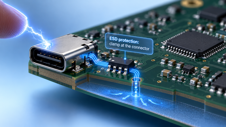
Figure 1: An ESD strike at a USB connector diverted through a TVS array to the ground
The diode is there to prevent a static discharge from picking up the protection. It goes into the board all at once along all paths and is divided into different paths depending on the impedance. This means that both the chip pin and the diode want the same current. The diode is either too far from the connector or grounded through a long, thin trace that leads to the chip. This guide explains how the clamp works, which parts are appropriate for each interface, which layout rules are used to keep the path short, and which checks are performed during fabrication.
What Is ESD Protection and Why Does a PCB Need It?
ESD protection consists of a set of components and copper to provide a lower-resistance path to ground than your ICs offer to ESD. A board requires this protection because the chip's protection level was designed for factory use, not for a person touching a connector while the board is charged.
How Electrostatic Discharge Affects PCBs
By moving, a person amasses charge. Dry air will hold that charge. The ESD Association cites 35,000 V for walking across carpet at 10 to 25% RH, but just 1,500 V at 65 to 90% RH. When that person touches a connector shell or an exposed pin, the charge escapes their body in nanoseconds.
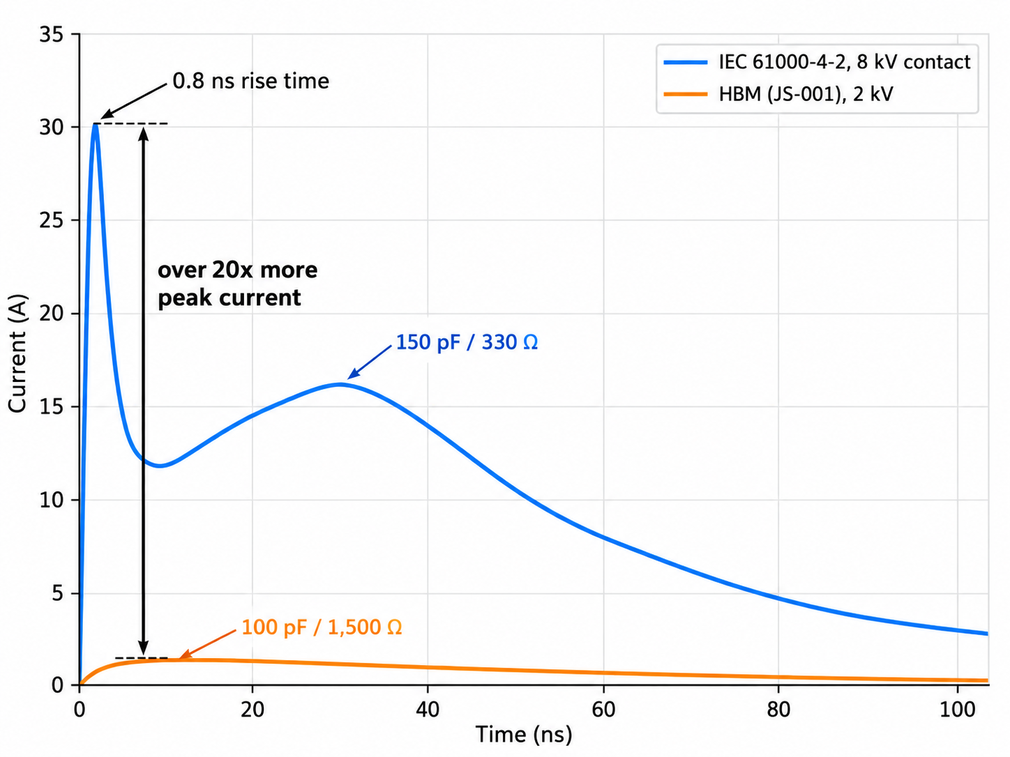
Figure 2: IEC 61000-4-2 8 kV contact discharge current compared with a 2 kV pulse
The current at the 8 kV contact level rises to nearly 30 A with a 0.8 ns rise time. Copper with an edge that fast is inductance and is an antenna. Thus, the pulse also enters traces that do not connect to the connector. We have written in more detail about the effect on electronics in our article. The 2 kV HBM rating equates to a peak current close to 1.3A. This is less than 1/20th of the pulsing power of the 8 kV system. Thus, a chip with an adequate HBM rating can still fail at a USB port.
What ESD Protection Is Designed to Prevent
ESD protection is designed to protect against 3 classes of failure, distinguished from each other in terms of when the failure is detected and its cost:
- Hard Damage: The pulse melts a junction or breaks a gate oxide, and the board is junk from the get-go.
- Latent damage: The part is weakened, but passes the test and fails later in service.
- Soft failures: components fail to operate normally, but the system resets, hangs, or scrambles data.
The cause of hard and latent damage is identical: current-through-silicon that was never sized for it. One fix addresses both: clamp the line below the IC's absolute max. Latent damage is more expensive due to shipping. According to the ESD Association, it is a fault or failure that manifests following a period of normal operation.
How Does a PCB ESD Protection Circuit Work?
A protection circuit is a shunt that remains inactive until the line voltage exceeds its breakdown voltage. For a few nanoseconds, it then becomes a low-impedance path to ground. The amount of the strike that it must take is determined by the surrounding copper.
Directing ESD Energy Away From Sensitive Circuits
A TVS diode is connected between the signal line and ground and is reverse-biased, making it virtually imperceptible at normal operating voltage. When the line is pushed past the breakdown point by a strike, the diode avalanches and conducts. The voltage left on the line is the breakdown voltage plus the pulse current times the dynamic resistance. Thus, the lower the dynamic resistance, the lower the residual will be.
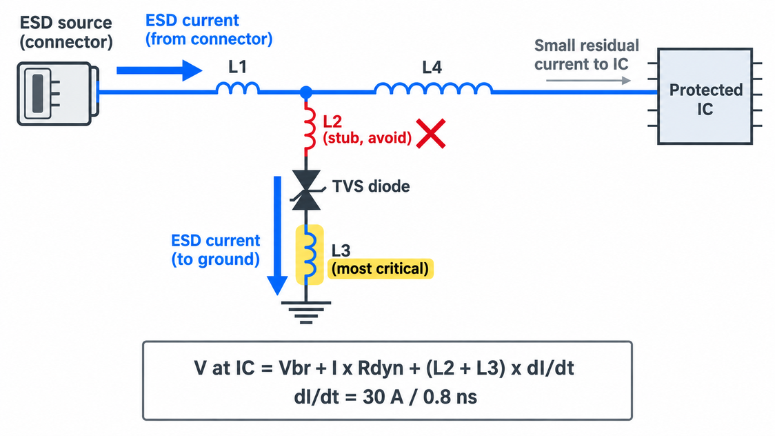
Figure 3: Current paths and parasitic inductances around a single-channel TVS diode
The ratio of the current into the TVS and the IC pin is proportional to the impedances of these branches. The TVS should be placed as close as possible to the connector, according to TI's ESD layout guide (SLVA680A). The protected IC is located far away, and the trace from the diode has more inductance. The pulse then selects the diode, and the process repeats.
Balancing Protection and Signal Performance
Each protection diode creates additional capacitance between the line and ground, since each time a diode conducts current, a real area is required. This is harmless on a slow line. With a fast line, the capacitance reduces the impedance in that area, causing part of each edge to reflect while the rest comes back rounded.
For instance, TI's TPD1E10B06 combines a typical capacitance of 12 pF with a typical dynamic resistance of 0.4 Ω for strong clamping and is rated for data rates up to 400 Mbps.
The diode's stand-off voltage sets the other limit: it should be greater than or equal to the line's peak voltage, or the diode will leak and clip the signal. The clamping voltage should not exceed the IC's absolute max. That right-hand portion is contained within that window.
Which ESD Protection Components Are Used on PCBs?
Nearly all the boards support three families of devices, each with a different capacitance/voltage relationship. The game interface that you are securing determines the trade that you can afford.
TVS Diodes and Other Common Protection Devices
The common board-level devices have different materials; hence, the clamping hardness of them is different:
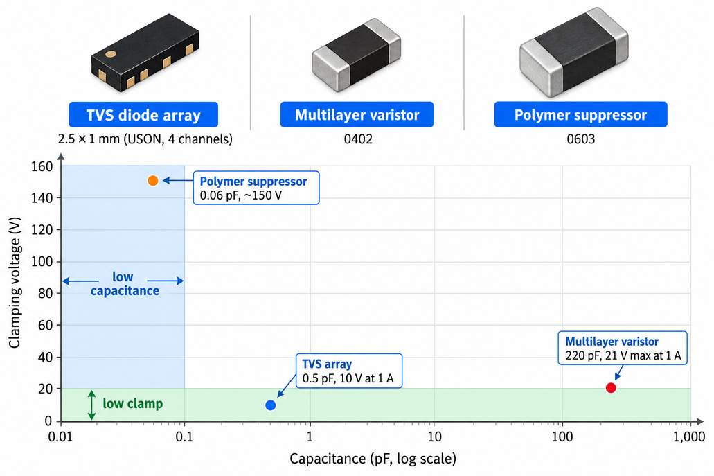
Figure 4: TVS diode, multilayer varistor, and polymer suppressor
- TVS diodes and diode arrays: silicon avalanche clamps with the lowest clamping voltage and sub-nanosecond response.
- Multilayer varistors: zinc oxide ceramic chips that are cheap, rugged, clamp higher, and provide more capacitance.
- Polymer ESD Suppressors: composite devices that have virtually no capacitance and a much higher clamping voltage.
The default is TVS diodes, as silicon will clamp at a very low level (e.g., the TP4E05U06 typically clamps at 10 V for a 1 A pulse). The SMAJ5.0A power TVS dissipates 400 W (10/1000 µs) on a 5 V power rail. Unidirectional parts work best for lines that never dip into the negative, while bidirectional parts, such as the TPD1E10B06, are well-suited for audio. TVS parts are listed under the other diode types in our diode type guide.
Selecting Components for Different Interfaces
Selection runs in a fixed order: working voltage first, then the capacitance the data rate tolerates, then the clamp level the IC survives. TI's USB application note (SLVAF82B) supplies the capacitance limits:
| Interface | Line Voltage or Data Rate | Selection Target | What to Fit |
|---|---|---|---|
| GPIO, buttons, audio | Slow, may swing both ways | Bidirectional TVS, capacitance not critical | TPD1E10B06 (12 pF typical), or an MLV on buttons |
| USB 2.0 D+ and D- | 480 Mbps, 3.3 V signaling | Stand-off of at least 3.3 V, under 4 pF | A low-capacitance TVS channel |
| USB 3.x SuperSpeed, HDMI 2.0 | 5 to 10 Gbps | Under 0.5 pF at 5 Gbps, under 0.3 pF at 10 Gbps | TPD6E05U06 (0.47 pF typical) on 5 Gbps lanes |
| USB VBUS, DC input | 5 V, up to 48 V with USB PD | Stand-off at or above the rail, surge rated | SMAJ5.0A on 5 V, TI TVS2200 on 20 V |
| Antenna feed | RF, any load detunes | Lowest possible capacitance | Polymer suppressor such as PGB1010603 |
The faster the line, the less capacitance you can spend, so the clamp you accept rises. Power rails also need surge capability, because unplugging a loaded cable rings the line.
How to Design ESD Protection for PCB Layout
ESD protection for PCB layout is all about inductance – the same diode can work well or poorly depending on the copper it is connected to. Each control places, grounds, and routes a portion of that inductance.
Component Placement and Short Discharge Paths
The branch with the placement determines which branch the strike reaches first, and the TVS is placed at the connector. JLCPCB's diode guide states that a TVS 15 mm (590 mil) away from a connector offers much less protection than one 2 mm (79 mil) away from the connector. The discharge route is kept short by three placement rules:
- TVS first on the line, meaning it must be placed in front of all other components, and the protected IC must be far removed from the TVS; the trace after the clamp will deter the pulse.
- Flow-through routing: run the signal straight through the TVS pad—since a branch or stub also adds its own inductance in series with the diode, it delays the clamp. That is the purpose of flow-through packages such as TPD4E05U06.
- If it is necessary to place the TVS on another layer, the following rules apply: No via before the clamp. The TI layout guide deems that order acceptable, and the other order is the worst case.
Grounding and Return Path Design
Often, the largest inductance in the protection path is the connection between the TVS ground pin and the plane. The suggested approach is to have a same-layer ground pour stitched to a plane on the next layer, with one via right next to the pin. Each additional millimeter here results in a higher clamp voltage since the entire pulse is delivered through it.
Grind the connector shell down to the same point as the strike first gets to it. A chassis screw adjacent to the TVS ground is provided for the strike to prevent much current from flowing across the logic ground. If none, the tightly coupled ground planes help to keep the ground shift small. Stitching and pour connections are discussed in our copper pour basics article. A slot or split causes the return current to flow around it, thereby introducing inductance where it is least desirable. TI also recommends large ground via pads and drills because a larger plated area reduces impedance at ESD frequencies.
Routing Sensitive Signals and Interfaces
Consider the space between the connector and the TVS a keep-out zone for unprotected traces. The entire ESD current passes through there before the clamp is activated, and it radiates. Then, a neighbor trace collects a pulse with no diode to impede the way.
Corners on the protected line are significant too: TI's simulation of an 8 kV strike shows at least 7 kV of field at corners with a 90° angle. This is sufficient to ionize the air at a radius <~ 2.6 mm (102 mil). Go straight as straight can go, go round where you must, and do not turn any corners tighter than 45°. Reset/clock lines require spacing from the board edge and connectors to prevent soft failures due to an upset. Place them on the board, cover them with ground, and reset the inputs at the IC.
How PCB Manufacturing Affects ESD Protection
The protection path is as good as the copper the fabricator uses, because inductance depends on the dimensions. The widths, vias, and dielectric thicknesses are all within tolerances, so the design should operate throughout that range.
Maintaining Layout, Trace, and Via Accuracy
Etched copper always differs a little from the Gerber, so the protection layout should never depend on an exact figure. These are standard values from the JLCPCB PCB capabilities page:
| Fabrication Parameter | JLCPCB Standard Value | What It Means for the ESD Path |
|---|---|---|
| Track width tolerance | ±20%, so 0.1 mm (4 mil) finishes at 0.08 to 0.12 mm (3.1 to 4.7 mil) | Draw TVS ground connections wide so the tolerance is negligible |
| Hole position tolerance | ±0.075 mm (3 mil) | Give the ground via pads a generous ring so the drill wand never breaks it |
| Average hole plating thickness | 18 µm (0.7 mil) | Several ground vias share the pulse current better than one |
| Via-in-pad | Epoxy or copper paste filled and capped, 0.15 to 0.55 mm (6 to 22 mil) via diameter | Let the ground via sit inside the TVS ground pad |
| Copper to the routed board edge | At least 0.2 mm (8 mil) | Edge copper meets air discharges first, so keep sensitive nets further in |
Via-in-pad matters most for small protection arrays. TI recommends a non-conductive filler, plated over the pad, so the drilled surface stays available for current. JLCPCB's epoxy-filled and capped process matches that description and is the default for boards with 6 or more layers.
Controlling Stackup and Ground Structures
The distance between the surface layer and the first ground plane determines the inductance of the TVS ground loop. In JLCPCB's standard 1.6 mm (63 mil) 4-layer stackup, JLC04161H-7628, the prepreg between the top layer and L2 is 0.2104 mm (8.3 mil). For a 2-layer board of the same thickness, the distance to the nearest plane is approximately 1.5 mm (59 mil).
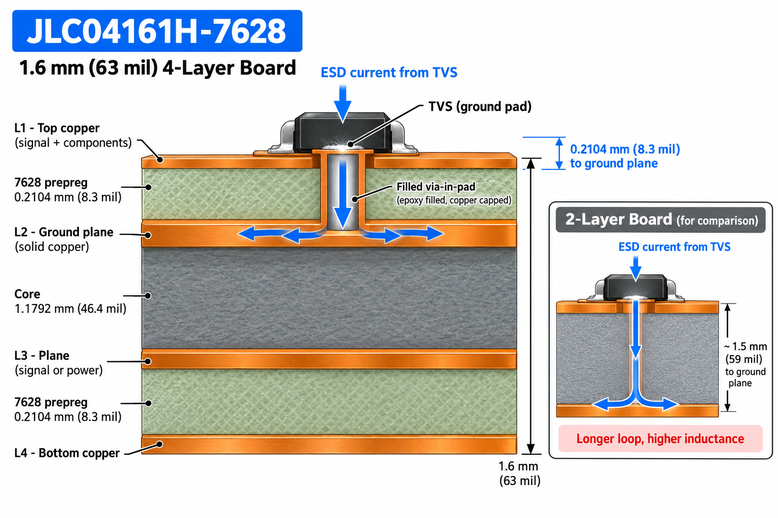
Figure 5: TVS ground path in a 4-layer stackup with a 0.2104 mm (8.3 mil) prepreg to the ground plane
This closer plane shortens the body and connects the upper ground plane to the inner plane. Thus, ground shift remains low throughout. JLCPCB claims that they produce their boards based solely on the published stackup. Therefore, the distance you plan for is the distance you will get. Controlled impedance should be part of the same decision, as the TVS pad introduces a small discontinuity on each protected high-speed line. Impedance control is available for JLCPCB boards with 4 to 32 layers, with a standard tolerance of ±10%. Maintaining target leaves makes more money for the protection device.
Inspection and Manufacturing Quality
A TVS ground that never plated through is a loss for the clamp, but doesn't alter the appearance of a board. According to the quality control page of JLCPCB, the bare-board checks are performed step by step:
- AOI after pattern plating: A camera checks the etched copper in great detail for defects.
- Flying probe electrical testing, which uses moving test probes to test the connectivity of each net.
- Shipping with final piece-by-piece quality checking.
Here, the flying probe step is important, as an open ground via interrupts a net that a camera cannot view. Bare-board testing verifies the path but cannot measure clamp performance.
FAQs About PCB ESD Protection
Q: Can a Zener diode replace a TVS diode for ESD protection?
Does every ESD protection diode need its own ground via?
Q: Does every ESD protection diode need its own ground via?
Ideally, yes, placed immediately beside the ground pin and tied to the adjacent plane. Sharing a via adds other current and extra trace length to the clamp path, which raises the voltage the protected IC sees.
Q: Can one TVS array protect both the USB data lines and VBUS?
It can if its stand-off voltage is at least the VBUS voltage. TI lists the 5.5 V TPD4E05U06 for D+, D-, and VBUS on 5 V USB 2.0 ports. A USB PD port that raises VBUS to 20 V needs a separate surge-rated TVS.
Q: Why does my board still reset during ESD testing with TVS diodes fitted?
The diodes stop damage, but the pulse can still couple into reset, clock, or ground nets. Look for unprotected traces near the connector, a long TVS ground connection, and an unfiltered reset input.
Conclusion
An ESD protection is a way, not a part. The diode sets the clamping behavior. However, it is the placement, a short ground connection, and a continuous plane that determine how much of the strike reaches the plane. This path must then be reproduced on the fabricated board. This is where wide ground copper, filled vias, and thin dielectric to the plane really pay off.
As interfaces transition to higher-speed lanes, the protection capacitance budget will continue to decrease, and layout will bear a greater burden. Once you have your layout, JLCPCB uses the published stackups to create multilayer boards and offers features such as via-in-pad, impedance control, and flying-probe testing.
Popular Articles
Keep Learning
Building Effective ESD Protection Into PCB Design
Key Takeaways Layout Rules: ESD spikes rise in nanoseconds; routing layout matters more than part specs alone. Clamp First: Place TVS diodes right at the connector using direct, flow-through traces. Low-Inductance Ground: Use short, wide traces with immediate ground vias to prevent voltage shifts. Capacitance Limits: Use low-capacitance clamps (< 0.5 pF) on high-speed lines like USB 3.x. DFM-Ready: Account for standard via and trace tolerances to ensure reliable board fabrication. ESD protection on a ......
Managing Skin Effect Loss in High-Frequency PCB Design
Key Takeaways Skin Depth Shrinks: High frequencies force current to the trace surface, shrinking depth to 0.66 µm at 10 GHz. Roughness Adds Loss: Copper foil roughness lengthens current paths, sharply increasing high-speed resistance. Plating Affects Signals: Low-conductive finishes like ENIG nickel increase attenuation on exposed lines. Wider Traces Help: Wider traces and thicker dielectrics lower conductor loss by expanding current surface area. Use Smooth Foils: Pairing low-profile copper foils (VL......
How Impedance Controlled Routing Delivers Reliable High-Speed PCB Performance
Key Takeaways Impedance Controlled Routing is essential for reliable high-speed PCB performance above 1 Gbps, eliminating reflections, ringing, and bit errors by precisely targeting interface-specific impedances (USB 90 Ω, PCIe 85 Ω, DDR4 40/80 Ω, HDMI 100 Ω) through field-solver calculations, symmetrical stackups with continuous reference planes, stable low-loss dielectrics, and strict single-ended/differential routing rules. Manufacturing precision in etching, copper profile, and lamination, verifie......
Getting PCB Characteristic Impedance Right for Reliable Signals
Key Takeaways Impedance Defined: Characteristic impedance is set by trace geometry and the reference plane, not by copper DC resistance. Core Factors: Trace width, copper thickness, dielectric height, and dielectric constant determine the impedance value. Reference Plane: High speed traces need a continuous reference plane to prevent signal reflection. Factory Verification: Fabricators adjust trace width and check impedance using time domain reflectometry on test coupons. Design Approach: Select a sta......
Stop PCB Crosstalk Before It Becomes a Signal Integrity Problem
Key Takeaways NEXT vs FEXT: NEXT saturates with trace length, while FEXT grows linearly with distance. Spacing & Stackup: Apply the 3W rule and keep traces close to reference planes. Edge Rates: Fast rise times drive crosstalk more than clock frequency. Fab Margins: Etching variations reduce gaps, requiring extra layout clearance. Verification: Use DFM checks and TDR coupons instead of basic continuity tests. PCB crosstalk is the noise one trace pushes into its neighbor, even though the two nets are e......
Navigating the Impedance Landscape: Selecting the Right Impedance for USB, Ethernet, HDMI, and SD Card Interfaces
Introduction In the realm of high-speed digital communication, choosing the right impedance is a critical aspect of successful PCB design. Impedance matching ensures optimal signal integrity, minimizes reflections, and enhances the overall performance of interfaces such as USB, Ethernet, HDMI, and SD Card. In this blog post, we'll explore the importance of impedance, the factors influencing impedance selection, and best practices for ensuring reliable data transmission in these widely used interfaces.......