Optimizing High-Voltage Circuit Safety with PCB Dielectric Strength
16 min
- Fundamentals of PCB Dielectric Strength and Insulation
- Key Factors Influencing PCB Dielectric Materials
- Testing and Qualification of PCB Insulation Performance
- Engineering Strategies for High-Voltage PCB Layouts
- JLCPCB's Advanced Material Selection & Quality Testing Standards
- FAQs about PCB Dielectric Strength
- Conclusion
Key Takeaways
- Non-linear Scaling: Dielectric strength drops as thickness increases.
- Safety vs Signals: Dielectric strength ensures safety, while Dk controls signal speed.
- Material Selection: High-voltage safety depends on Tg, CTI, and moisture resistance.
- Spacing Rules: Clearance prevents air arcs, while creepage prevents surface tracking.
- Assembly Testing: Hi-pot testing requires finished assemblies, not bare boards.
Dielectric strength is the number engineers quote to prove a board is safe at mains voltage. It is also the number most often used wrongly. A laminate datasheet lists dielectric strength in kilovolts per millimeter. With a 1.6 mm (63 mil) board, it is tempting to simply multiply the value by the board thickness.
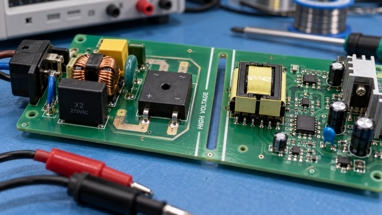
Figure 1: PCB showing an isolation slot milled between primary and secondary copper
And the same arithmetic fails, because breakdown never averages across a material. It hunts for the weakest path through it, and a thicker slab holds more resin, more glass bundles, and more voids along the way. Once kV/mm stops being a multiplier, high-voltage work becomes a spacing and materials problem again. This guide covers how dielectric strength is measured and how it differs from dielectric constant. It then compares FR-4, high-Tg, and ceramic substrates, and turns clearance and creepage rules into millimeters on your layout.
Fundamentals of PCB Dielectric Strength and Insulation
Insulation on a printed board is judged by two numbers that sound alike. They answer different questions, because one belongs to the material and the other belongs to the object you built from it.
What is Dielectric Strength and How Is It Measured?
Dielectric strength is the maximum electric field an insulator holds before it starts conducting. It is a field rather than a voltage, so it carries units of kV/mm or V/mil.
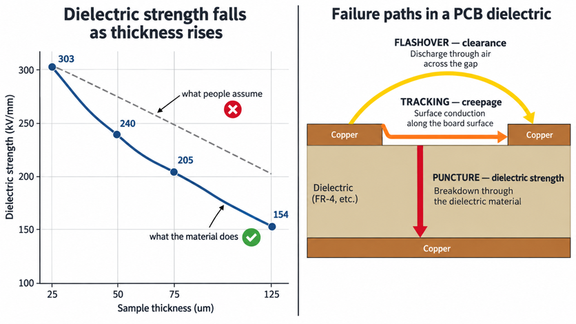
Figure 2: Dielectric strength falling as sample thickness rises
Laminate suppliers measure it two different ways, and confusing them is the most common error in material selection.
- Electric Strength — IPC-TM-650 2.5.6.2: Measures breakdown perpendicular to the laminate layers, through the board thickness. The result is reported as an electric field, usually in kV/mm. IPC-4101 sheets often specify a minimum of 30 kV/mm.
- Dielectric Breakdown — IPC-TM-650 2.5.6: Measures failure parallel to the laminate layers, along the glass and resin. The result is reported as a single voltage in kV. For example, Kingboard KB-6165F lists 65 kV for this test, but that value should not be applied directly to a thin prepreg layer.
Measured values generally decrease as the specimen thickens, even when the material is identical.
| Film Thickness | Dielectric Strength (ASTM D149) | Voltage It Actually Holds | What This Tells You |
|---|---|---|---|
| 25 µm (1 mil) | 303 kV/mm | about 7.6 kV | Thin barriers punch far above their weight |
| 50 µm (2 mil) | 240 kV/mm | about 12 kV | Doubling the thickness adds only 58% more voltage |
| 75 µm (3 mil) | 205 kV/mm | about 15.4 kV | The curve is already flattening hard |
| 125 µm (5 mil) | 154 kV/mm | about 19.3 kV | Five times the thickness, 2.5 times the voltage |
Thickness buys real withstand voltage, but it buys progressively less of it. So a kV/mm figure measured on one sample cannot be scaled to a different geometry.
PCB Dielectric Strength vs. PCB Dielectric Constant
The PCB dielectric constant, denoted as Dk, measures how much charge a material stores per unit voltage. It has nothing to do with insulation safety. Dk sets how fast a signal travels and what impedance a trace presents, which is why it lives in the signal-integrity half of a datasheet. These properties describe different behaviors, so they are measured differently and should not be treated as interchangeable.
- Permittivity (Dk) and loss tangent (Df): Measured using IPC-TM-650 2.5.5 methods. A small AC field is applied, and the material’s electrical response is measured without destroying the sample.
- Electric strength: Measured using IPC-TM-650 2.5.6.2. The voltage is increased until the laminate breaks down, so the test is destructive.
Loss tangent, or Df, tells you how much electrical energy is converted into heat. It is therefore mainly a signal-loss parameter, not an insulation-safety value. Standard FR-4 may have a Dk around 4.4 at 1 GHz, but neither Dk nor Df tells you whether a high-voltage gap will arc.
Higher Dk can even make high-voltage behavior slightly worse by concentrating electric fields around sharp copper edges. The effect is usually much smaller than spacing and geometry, but it is still worth understanding.
Key Factors Influencing PCB Dielectric Materials
Material choice for a high-voltage board is rarely won on kV/mm alone. The substrate with the highest field strength is often the wrong one, because thermal survival and surface tracking usually decide the outcome.
Comparative Analysis of Common PCB Substrates (FR-4, High-Tg, Ceramic)
Standard FR-4 covers most mains-voltage work, and it does so honestly. Woven glass in an epoxy matrix yields a through-thickness field strength of approximately 30-40 kV/mm.
Ceramic is where the intuition breaks most sharply. A 96% alumina substrate, such as CoorsTek AD-96, sits near 8.3 kV/mm, which is well below plain FR-4. It is still the material of choice in demanding power modules, because it wins on thermal conductivity, dimensional stability, and the fact that inorganic ceramics do not carbon-track at all.
| Substrate | Typical Electric Strength | Dk (approx.) | Tracking Behaviour | Where It Earns Its Place |
|---|---|---|---|---|
| Standard FR-4, Tg 130 to 150 | 30 to 40 kV/mm | 4.4 to 4.6 | Group IIIa, CTI 175 to 249 V | Almost all mains-connected consumer and industrial boards |
| High-Tg FR-4, Tg 170 | 30 to 40 kV/mm | 4.3 to 4.5 | Group IIIa unless a high-CTI grade is specified | Hot enclosures, thick multilayers, long thermal life |
| Polyimide film, flex | 154 to 303 kV/mm by gauge | 3.4 to 3.5 | Excellent, but thin and easily damaged | Thin isolation barriers and flex tails inside power products |
| Aluminium IMS | The dielectric layer withstands nearly 3 kV | not specified | Dielectric is buried, so tracking is not a risk | LED and power stages where heat matters more than voltage |
| 96% alumina ceramic | about 8.3 kV/mm | about 9 | Does not track, being inorganic | Power modules, high temperature, harsh chemistry |
Impact of Operating Temperature, Moisture, and Layer Thickness
Temperature attacks insulation through the resin rather than the glass. Once the board runs near its glass transition temperature, the epoxy softens, and insulation resistance falls with it. Keeping the continuous operating temperature 20 to 30 °C below Tg is the practical guard band, which is why selecting the Tg of your PCB belongs early in a high-voltage project.
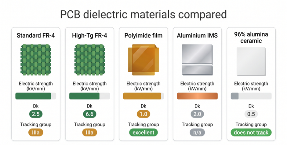
Figure 3: Field strength, Dk, and tracking behavior compared
- Moisture is the quieter problem: FR-4 absorbs only about 0.1-0.2% of its weight in water. That water sits in the resin, and along the glass interfaces where the field is strongest, and published work puts the resulting loss of dielectric strength as high as 20%. So a board qualified in a dry lab can behave differently inside a humid pump housing.
- Layer thickness matters in a way the datasheet hides: Your real insulation between two inner-layer nets is one or two prepreg plies, often 0.1 mm (4 mil) rather than the full board. A resin-poor style, such as 7628, fills differently from a thin 1080 ply, so the pressed result varies with the copper above and below it.
Testing and Qualification of PCB Insulation Performance
Testing insulation splits into two jobs that get confused constantly. One measures a material property in a laboratory, while the other proves that a finished assembly survives a defined stress.
Executing a Standardized Dielectric Strength Test (Hi-Pot Testing)
A hi-pot test, short for high potential, is a dielectric withstand test rather than a measurement. You apply a defined voltage across an isolation barrier for a defined time and watch the leakage current. The answer is a pass or a fail, so it never produces a kV/mm figure and was never meant to.
The actual test voltage comes from the applicable safety standard, but a common rule for mains equipment is 2× the working voltage + 1000 V AC. Qualification testing typically applies that voltage for 60 seconds. Production testing often uses a shorter test to avoid repeatedly stressing otherwise good insulation.
The basic test sequence is the same for a bare PCB or a finished assembly.
- Identify the barrier under test and short every net on each side together, so the tester sees two nodes rather than a hundred.
- Set the leakage trip threshold before applying voltage, typically a few milliamps, once the Y-capacitors are removed.
- Ramp the voltage rather than switching it on, since a hard step delivers a capacitive surge that trips a healthy board.
- Hold at the target voltage for the specified dwell, watching for leakage that climbs rather than settling.
- Ramp back down and confirm the barrier is discharged, because a 1.6 mm (63 mil) board is still a capacitor.
Identifying Insulation Breakdown and Creepage Risks
Insulation fails along three separate paths, each with its own rule. Puncture goes straight through the dielectric, which is what dielectric strength describes. Flashover jumps through the air and is governed by clearance, while tracking crawls across the surface and is governed by creepage.
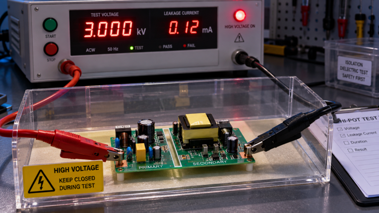
Figure 4: A hi-pot tester performing a dielectric withstand test on a mains-input PCB
The comparative tracking index (CTI) measures how well an insulating material resists surface tracking, using the IEC 60112 test. IEC 60664-1 then places materials into four groups based on their CTI value. That material group is used to determine the required creepage distance for the insulation system.
- Group I, CTI of 600 V and above, allows the shortest creepage distances for a given working voltage.
- Group II, CTI from 400 V up to 600 V, sits between the extremes and covers many upgraded laminates.
- Group IIIa, CTI from 175 V up to 400 V, is where ordinary FR-4 lands, so it is your default unless you specify otherwise.
- Group III b, CTI from 100 V up to 175 V, also applies whenever a material has no declared CTI at all.
Flux residue and dust accelerate all of it, which is what the pollution degree exists to capture, so choosing the right CTI value matters as much as choosing a thickness.
Engineering Strategies for High-Voltage PCB Layouts
All of this becomes useful only when it turns into millimeters in your design rules. Two standards do that job; they answer different questions, and a safe layout satisfies both.
Clearance and Creepage Distance Optimization Rules
Clearance is the shortest distance through air between two conductors. Creepage is the shortest distance along the surface of the insulation between the same two conductors. They are set by different physics, so they take different inputs.
Clearance is dimensioned against a short transient, whereas creepage is dimensioned against the working voltage that sits there for years. So clearance depends on rated impulse voltage, pollution degree, and altitude, while creepage depends on RMS working voltage, pollution degree, and material group. Creepage must never be smaller than clearance, so on a compact board, the creepage rule usually determines the gap. The table below carries the three columns you will actually use, and treating PCB voltage clearance as a per-layer rule is what makes it workable.
| Working Voltage | B1 Internal Conductors | B2 External, Uncoated | B4 External, Under Solder Mask | What It Means on Your Layout |
|---|---|---|---|---|
| 0 to 15 V | 0.05 mm (2 mil) | 0.10 mm (4 mil) | 0.05 mm (2 mil) | Your default DRC clearance already covers this |
| 31 to 50 V | 0.10 mm (4 mil) | 0.60 mm (24 mil) | 0.13 mm (5 mil) | First point where bare outer copper needs its own rule |
| 101 to 150 V | 0.20 mm (8 mil) | 0.60 mm (24 mil) | 0.40 mm (16 mil) | Rectified 120 V rail, where the mask buys back most of the space |
| 171 to 250 V | 0.20 mm (8 mil) | 1.25 mm (49 mil) | 0.40 mm (16 mil) | 230 V mains input on a charger or appliance board |
| 301 to 500 V | 0.25 mm (10 mil) | 2.50 mm (98 mil) | 0.80 mm (31 mil) | 400 V DC link behind a PFC front end |
| Above 500 V | add 0.0025 mm per volt | add 0.005 mm per volt | add 0.00305 mm per volt | An 800 V bus needs about 4 mm (157 mil) of bare outer spacing. |
Inner-Layer Isolation Protocols in Multi-Layer Boards
Inner layers are governed by dielectric spacing rather than creepage. There is no air path and no contamination between the two buried layers. A typical four-layer stackup leaves roughly 0.1 mm (4 mil) of prepreg between an outer layer and the adjacent plane.
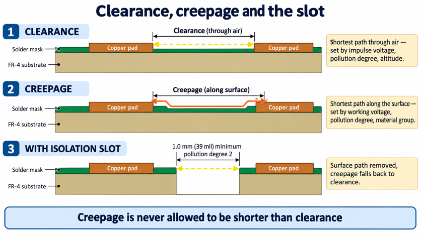
Figure 5: Clearance, creepage, and the effect of a milled isolation slot
For example, a 400 V potential across that gap produces a field near 4 kV/mm, which is comfortable for FR-4 but far tighter than the board thickness suggests. Two prepreg plies instead of one is the standard defense, because a single ply can develop a resin-starved region over dense copper.
Copper on every layer has to respect the same barrier, and this is the mistake that survives review most often. A ground plane poured to the board edge quietly bridges an isolation gap you drew carefully on the top layer. So the keepout has to be cut through all layers, including planes, thermal reliefs, and any stitching vias near the boundary.
JLCPCB's Advanced Material Selection & Quality Testing Standards
A manufacturer contributes two things to insulation performance. One is the laminate that presses into your board, and the other is the evidence it can hand you about that laminate.
High-Quality Insulating Laminates and Rigorous Material Traceability
JLCPCB builds standard FR-4 orders on Grade A laminates from Nan Ya, Kingboard, and Shengyi. It publishes the actual datasheets rather than describing them generically, so you can read the numbers yourself. The JLCPCB certifications page carries sheets for Nan Ya NP-140F and NP-155F, Kingboard KB-6164 and KB-6165F, and Shengyi S1141, S1000H, and S1000-2M at Tg 170.
That matters because those sheets contain what a safety file needs. KB-6165F is a mid-Tg grade at 150 °C, with a comparative tracking index above 175 V and a dielectric breakdown of 65 kV on the parallel test. Writing that grade into your fabrication notes is meaningfully different from writing FR-4 and hoping.
Comprehensive High-Voltage Insulation and Dielectric Testing
Every bare board is electrically tested before it ships, using a flying probe for prototypes and a fixture for volume runs. That test drives every net against the netlist and checks continuity and isolation. It is not a hi-pot test, and treating it as one would be a mistake. Bare-board electrical test confirms that the two nets are separate at low voltage. A dielectric withstand test confirms that the separation holds at several kilovolts, which is a different question, and JLCPCB does not publish that as a service on customer boards.
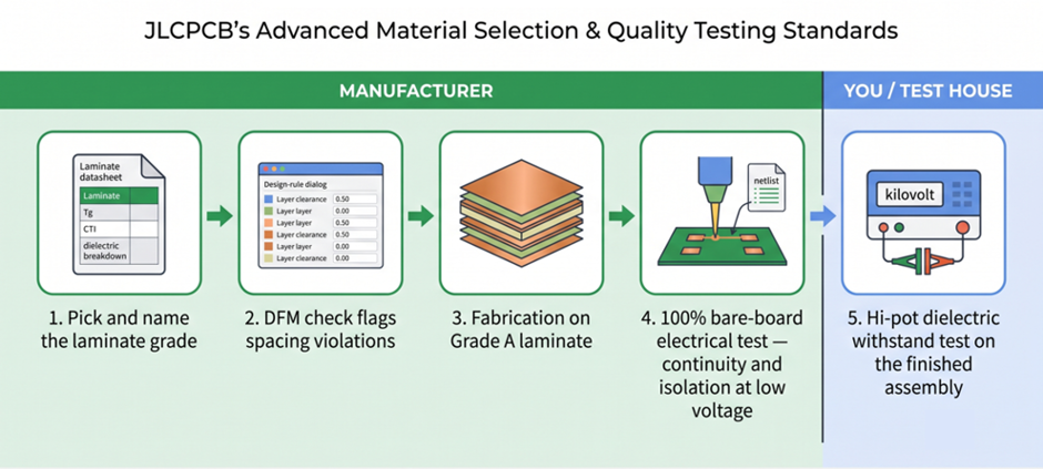
Figure 6: Showing where fab testing ends and compliance testing begins
So the routine hi-pot on your finished assembly belongs to you or to a compliance test house. The design work described earlier is what makes it pass. The rest is a design decision you can make today. Set your clearance rules per layer, draw the isolation barrier across the whole stackup, name the laminate grade in your notes, then upload your high-voltage design and read the DFM report before you commit to a build.
FAQs about PCB Dielectric Strength
Q: Can I multiply a laminate's kV/mm rating by my board thickness to get a working voltage?
No, because dielectric strength falls as the sample gets thicker. The figure only applies to the geometry it was measured on. Size your gaps from IPC-2221C and IEC 60664-1, then confirm the barrier with a hi-pot withstand test.
Q: Does a higher PCB dielectric constant mean better insulation?
No. Dielectric constant describes how much charge the material stores, so it controls signal speed and trace impedance rather than breakdown. A higher Dk slightly concentrates the field at sharp copper edges, which works against you at high voltage.
Q: Does solder mask count as insulation when I calculate creepage?
It depends on which standard you are answering to. IPC-2221C allows reduced spacing under a permanent polymer coating, but IEC 60664-1 measures creepage across the bare surface unless the coating qualifies under IEC 60664-3. For safety-critical barriers, design as if the mask is not there.
Q: Does JLCPCB hi-pot test my boards?
No. JLCPCB runs a full bare-board electrical test, which checks continuity and isolation against your netlist at low voltage, plus automated optical inspection. A dielectric withstand test at kilovolt levels is a separate operation, carried out by you or a compliance test house on the finished assembly.
Conclusion
Dielectric strength earns its reputation as a safety number only when you read it as a material property. The laminate tells you how hard the resin resists a field, while the geometry decides what field it will actually see. Those two only meet through the spacing tables, which is why a 1.6 mm board and a 0.1 mm prepreg ply can share a datasheet and behave nothing alike.
The habits that follow are cheap to adopt. Separate clearance from creepage in your design rules, and name the laminate grade instead of writing FR-4. Treat the solder mask as manufacturing protection rather than safety insulation, and keep the operating temperature well below Tg. JLCPCB's published laminate datasheets and DFM checks make the material half straightforward, so your attention can go to the spacing.

Keep Learning
Optimizing High-Voltage Circuit Safety with PCB Dielectric Strength
Key Takeaways Non-linear Scaling: Dielectric strength drops as thickness increases. Safety vs Signals: Dielectric strength ensures safety, while Dk controls signal speed. Material Selection: High-voltage safety depends on Tg, CTI, and moisture resistance. Spacing Rules: Clearance prevents air arcs, while creepage prevents surface tracking. Assembly Testing: Hi-pot testing requires finished assemblies, not bare boards. Dielectric strength is the number engineers quote to prove a board is safe at mains ......
How Copper Foil Shapes PCB Performance and Manufacturing Quality
Key Takeaways Weight: 1 oz copper ≈ 35 µm thickness; higher weight increases current capacity. Types: ED for standard rigid boards, RA for dynamic flex circuits. DFM & Loss: Smoother foil lowers RF loss; thicker foil requires wider trace spacing. The part of a PCB that actually carries the electrical signal is the copper foil. The strength comes from the glass weave, the resin is used to keep the layers together, and the solder mask is used to provide protection and separation of exposed copper. But w......
A Complete Guide to Copper Clad Laminate (CCL) in PCB Manufacturing
Key Takeaways CCL is the base material: a cured resin-reinforcement sheet with copper foil bonded to one or both sides. Three parts control performance: Resin affects heat and loss, reinforcement controls stability, and copper foil affects conductor behavior. Choose by the main design stress: Heat, frequency, and cost usually determine the best laminate family. Slash sheets define the material: IPC-4101 uses numbered slash sheets to specify rigid PCB base materials. Tg alone is not enough: Td and time......
Buried Vias in Advanced PCBs: Enabling Higher Density, Better Signal Integrity, and Compact Designs
Key Takeaways Hidden Routing: Buried vias connect only inner layers, keeping outer surfaces clear for dense components and traces. Better Signal Integrity: They eliminate via stubs, reducing parasitics and signal loss in high-speed designs. Higher Density: Essential for HDI boards, dense BGAs, and small form factors like wearables. Higher Cost: Sequential lamination and extra drilling steps make them ~3×-4× more expensive than standard through-holes. Ever wondered how a modern smartphone mainboard can......
Unlocking Higher Density and Better Performance with Blind Vias in HDI PCBs
Key Takeaway Higher Density: Connects surface to inner layers without penetrating the whole board, freeing routing channels under fine-pitch BGAs. Improved Signal Integrity: Reduces via stub length to minimize impedance discontinuities in high-speed designs. Aspect Ratio Rule: Keep the depth-to-diameter ratio near 0.75:1 (max 1:1) for reliable laser drilling and void-free plating. Thermal Efficiency: Supports via-in-pad setups for better heat dissipation and compact component placement. Ever wonder ho......
How to Select Tg of PCB ?
What is the Tg of PCB? In PCB manufacturing, "Tg" stands for Glass Transition Temperature. It is the temperature at which the PCB substrate material transitions from a rigid, glassy state to a soft, rubbery state. PCBs are flame-retardant (UL94 V-0) and do not burn easily; instead, they soften above Tg. The Critical Correlation Between Tg and Z-Axis CTE (Coefficient of Thermal Expansion) When the temperature exceeds the Tg point, the PCB substrate material (such as standard FR-4) undergoes a physical ......