Stop PCB Crosstalk Before It Becomes a Signal Integrity Problem
19 min
- What Is Crosstalk in a PCB?
- Understanding Crosstalk in PCB Design
- The Design Factors That Increase PCB Crosstalk
- How to Evaluate PCB Crosstalk
- Practical PCB Crosstalk Prevention Techniques
- From Crosstalk Control to Manufacturable PCB Design
- How Professional PCB Manufacturers Support Crosstalk-Sensitive Designs
- FAQ About PCB Crosstalk
- Conclusion
Key Takeaways
- NEXT vs FEXT: NEXT saturates with trace length, while FEXT grows linearly with distance.
- Spacing & Stackup: Apply the 3W rule and keep traces close to reference planes.
- Edge Rates: Fast rise times drive crosstalk more than clock frequency.
- Fab Margins: Etching variations reduce gaps, requiring extra layout clearance.
- Verification: Use DFM checks and TDR coupons instead of basic continuity tests.
PCB crosstalk is the noise one trace pushes into its neighbor, even though the two nets are electrically isolated. You never draw that connection, and it never appears in the netlist, but the copper creates it anyway.
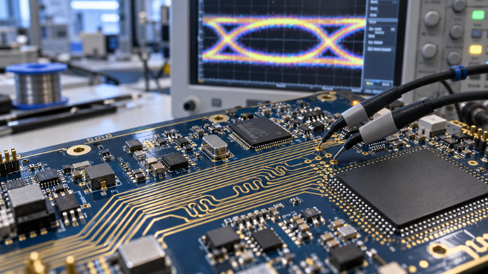
Figure 1: Densely routed high-speed PCB
A trace does not really carry a signal on its own. It carries a time-varying electric and magnetic field that wraps around the copper. Those fields do not stop at the edge of the trace, so any conductor sitting inside them takes a share. This guide covers the two coupling mechanisms and why near-end and far-end crosstalk behave in opposite ways. It also covers what a crosstalk calculator can and cannot tell you, plus the spacing, stack-up, and fabrication rules that keep coupled noise inside your budget.
What Is Crosstalk in a PCB?
Two traces that never touch can still share energy. The amount they share scales with how fast your signals switch.
What Is Crosstalk and Why Does It Occur?
Crosstalk is the unwanted transfer of energy from an active net into a quiet one. Engineers call the active net the aggressor and the quiet one the victim. The transfer happens through the fields around the copper, not through any conductive path, so no design rule check will ever flag it.
Because it is field coupling, only a changing signal couples anything. For example: A steady 3.3 V rail beside a clock line injects nothing into that clock. The clock injects noise into the rail on every edge. Stop the switching, and the crosstalk stops with it. Mutual capacitance links the traces through the electric field between them. Mutual inductance links them through the magnetic loop that the aggressor's current creates. Every parallel pair on your board has both, but most layout tools model neither.
How PCB Crosstalk Affects Signal Quality
Coupled noise attacks a digital receiver in two ways at once. It eats the static noise margin between the logic threshold and the signal level. It also shifts the moment the victim's edge crosses that threshold, so it shows up as timing jitter.
Modern interfaces have far less margin to give away than older ones did. A 3.3 V LVCMOS receiver sits about 1.3 V above its 2.0 V input high threshold, so a 50 mV glitch is harmless there. The failures crosstalk causes are the ones that look random on the bench:
- Jitter on a clock that only appears while the neighboring memory bus is active
- An eye diagram that closes vertically and horizontally at the same time
- A reset or interrupt line that glitches during a burst transfer, but never in idle
- An ADC whose bottom one or two bits rattle when nothing analog has changed
- A design that worked as a prototype and fails once the final revision is routed densely
Every symptom in that list is intermittent because the aggressor has to be switching for the fault to exist. That is why crosstalk gets diagnosed late, and usually after boards have shipped.
Understanding Crosstalk in PCB Design
Crosstalk arrives through two physical paths and leaves through two different doors. Knowing which door the noise leaves by tells you whether more spacing or a shorter parallel run is the fix.
Capacitive and Inductive Coupling
Capacitive coupling comes from the small capacitance between two adjacent traces. When the aggressor's voltage changes, that capacitance passes a current into the victim. The size of that current is the mutual capacitance multiplied by the rate of change of voltage. It has no preferred direction, so it splits evenly toward both ends of the victim.
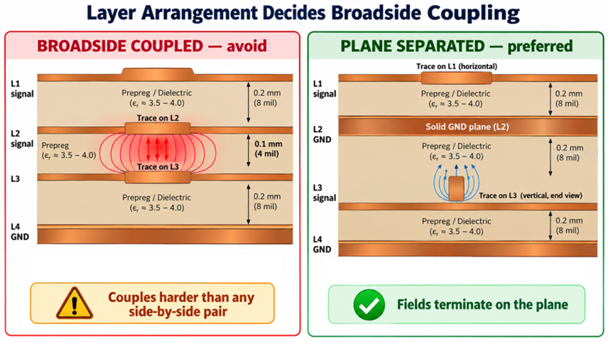
Figure 2: Cross-section showing mutual capacitance and mutual inductance
Inductive coupling works on current instead of voltage. The aggressor's current wraps the trace in a magnetic field. Part of that field threads the loop formed by the victim and its return path, so Faraday's law induces a voltage in the victim. The faster the aggressor's current changes, the larger that voltage gets.
Near-End and Far-End Crosstalk
Near-End Crosstalk:
Near-end crosstalk (NEXT) travels backward along the victim toward its driver. Its amplitude comes from the sum of the capacitive and inductive coupling ratios. It remains roughly constant while the aggressor's edge is within the coupled region. NEXT stops growing past a certain parallel length, which surprises people the first time they meet it. Noise generated at each point travels back and arrives spread over twice the one-way delay. Once the coupled length passes half the physical length of the rise time, extra length only widens the pulse.
Example: A signal covers about 6 ps per mm on FR-4 microstrip, so a 500 ps edge occupies roughly 83 mm (3.3 in) of copper. NEXT therefore, saturates near 42 mm (1.65 in) of parallel run. Beyond that point, doubling the run widens the pulse without raising its height.
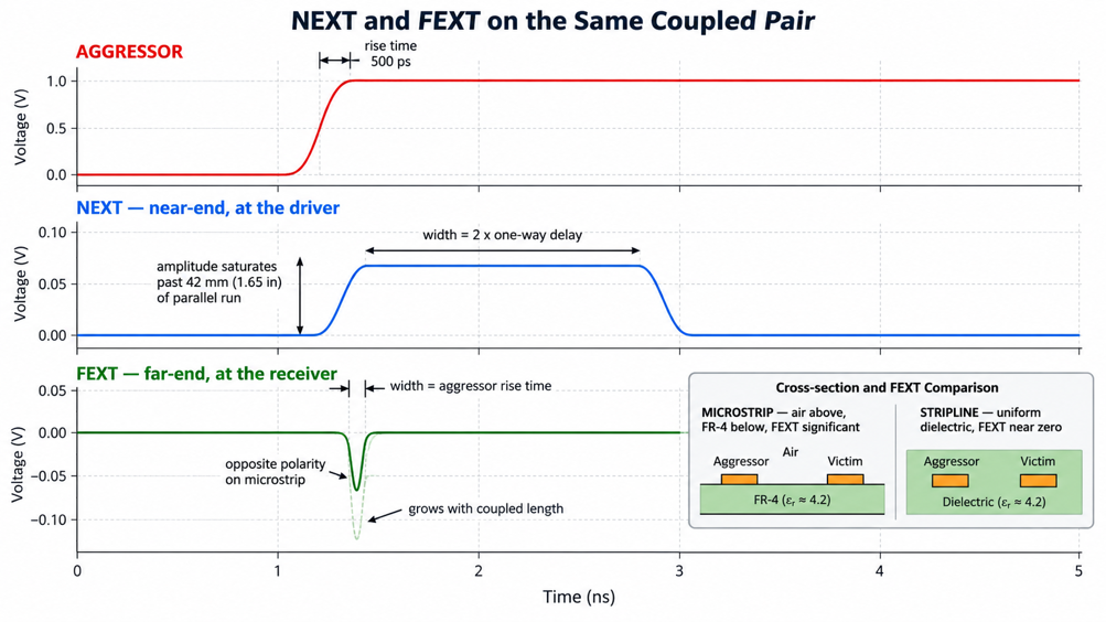
Figure 3: Timing diagram comparing a saturated NEXT pulse against a growing FEXT
Far-End Crosstalk:
Far-end crosstalk, or FEXT, behaves in the opposite way. It travels alongside the aggressor's edge at the same velocity, so every contribution reaches the receiver together and adds. FEXT therefore grows with the coupled length and shrinks with a slower edge. Its pulse is only as wide as that edge. FEXT depends on the difference between the inductive and capacitive coupling ratios, not on their sum. A stripline trace is buried in one uniform dielectric, which makes those two ratios essentially equal. The difference collapses, so far-end crosstalk on an inner layer approaches zero.
Example: A microstrip has FR-4 below the trace and air above it. That asymmetry leaves inductive coupling dominant, so the two terms no longer cancel. FEXT survives on an outer layer as a narrow pulse of opposite polarity to the aggressor's edge.
| Behaviour | Near-End Crosstalk (NEXT) | Far-End Crosstalk (FEXT) | What These Changes Mean in Your Layout |
|---|---|---|---|
| Where it appears | At the driver's end of the victim | At the receiver end of the victim | Probe the correct end before you trust a measurement |
| Coupling terms | Capacitive and inductive add | Capacitive and inductive subtract | FEXT can vanish entirely, NEXT never does |
| Effect of parallel length | Saturates past about 42 mm (1.65 in) for a 500 ps edge | Grows linearly with length, with no ceiling | Shortening a 200 mm (7.9 in) run fixes FEXT, not NEXT |
| Pulse width | Twice the one-way delay of the coupled section | Equal to the aggressor's rise time | A long run turns NEXT into a wide, slow disturbance |
| Microstrip vs stripline | Present in both, at a similar magnitude | Near zero in stripline, significant in microstrip | Bury long parallel high-speed runs between planes |
| Strongest lever | Spacing relative to dielectric height | Spacing, coupled length, and edge rate together | Spacing helps the bot; length only helps one |
The Design Factors That Increase PCB Crosstalk
Coupling is set by geometry and by edge rate. A router will happily wreck both while reporting a clean design rule check, so these are the parameters worth watching.
Trace Spacing, Parallel Routing, and Layer Arrangement
Spacing has the strongest effect on crosstalk. Once two traces are separated by more than about one trace width, coupling drops quickly. Doubling the gap can reduce coupled noise by roughly four times rather than two.
Figure 4: Coupling between adjacent signal layers versus a plane-separated stack-up
Parallel length also matters, but not equally for every type of crosstalk. Near-end crosstalk eventually reaches a limit, while far-end crosstalk continues to increase with length. That makes a long parallel run on an outer layer more troublesome than the same run in stripline. Layer arrangement can be even more important on dense boards. Traces placed directly above each other on adjacent signal layers can couple across their full width, especially when the dielectric between them is thin.
Two simple rules help:
- Route adjacent signal layers in different directions to minimize overlap.
- If parallel routing on adjacent layers is unavoidable, offset the traces laterally instead of stacking them directly above each other.
Signal Rise Time, Impedance, and Reference Planes
Edge rate matters more than clock frequency. A 74HC244 may switch with edges around 5 ns, while a 74LVC244 can switch in under 2 ns. The faster edge can produce much more crosstalk even if the PCB layout and clock frequency stay unchanged.
- Characteristic impedance also affects coupling: Higher-impedance traces usually sit farther from the reference plane relative to their width, allowing more of the electric field to spread sideways. Lower-impedance traces keep more of that field close to the plane.
- Dielectric height is especially important: Crosstalk depends strongly on trace spacing relative to the distance from the trace to its reference plane. Reducing that distance can greatly reduce coupling. This is why moving from two layers to four often gives a major improvement. A four-layer board can place a solid reference plane much closer to the signal traces.
- None of this works well with a broken return path: A slot or gap in the reference plane forces return current to detour, increasing shared impedance and coupling. Keep a continuous reference plane beneath high-speed signals whenever possible.
How to Evaluate PCB Crosstalk
You can put a number on crosstalk before the board exists, provided you know where the number came from. A calculator answers a narrow question in seconds, while a field solver answers a much broader one.
Using a PCB Crosstalk Calculator
A PCB crosstalk calculator is a form sitting on top of a two-dimensional field solver. You supply the cross-section: trace width, copper thickness, edge-to-edge spacing, dielectric height, and dielectric constant. The solver extracts the per-unit-length capacitance and inductance, then reports NEXT and FEXT as a percentage of the aggressor's swing.
JLCPCB does not publish a crosstalk calculator. Its two public calculators are the impedance calculator and the PI stiffener calculator. Settle your cross-section first with the JLCPCB Impedance Calculator, since it works from real pressed stack-ups. Then feed those dimensions into your EDA suite's field solver or a reputable third-party estimator.
Whichever tool you use, the answer rests on assumptions your board will break:
- Exactly two conductors, one aggressor and one victim, parallel for the whole coupled length
- A perfectly continuous reference plane beneath both traces
- A rectangular trace cross-section, so no etch taper is modeled
- One dielectric constant at one frequency, with no glass weave texture
- Ideal terminations at both ends of the victim, and no vias, bends, or connectors
The two-conductor assumption is the one that bites hardest. A DDR4 byte lane puts eight aggressors around one victim, and their contributions add. A calculator reporting a comfortable 3% for a single neighbor can therefore understate the real figure several times over.
When Simulation and Engineering Analysis Are Needed
A crosstalk budget turns a vague worry into a pass-or-fail number. Allocate a fixed share of the receiver's noise margin to coupled noise, typically around 5% of the swing for 50-ohm single-ended buses. Everything after that becomes a comparison against one figure.
A calculator is enough while the situation stays simple. Escalate to a full simulation once any of these appear.
- Several aggressors surrounding one victim, as on any parallel bus
- A coupled region that passes through a via field, a connector, or a package escape
- A victim that is a clock, a reset line, or an analog input, where one glitch is fatal
- A guard structure whose stitching you need to verify, rather than assume
- A noise budget already spent, leaving under about 2% of the swing for coupling
A 2D solver handles long, uniform coupled sections quickly and cheaply. A 3D solver is what you need for breakout regions, via transitions and package escapes, because those structures vary in all three dimensions.
Practical PCB Crosstalk Prevention Techniques
Prevention comes down to three levers: more distance between the traces, less distance to the reference plane, and less time running in parallel.
Increasing Trace Spacing and Reducing Parallel Runs
The 3W guideline is the rule everyone quotes and few state precisely. In its usual form, the 3W spacing is measured center-to-center. That works out as an edge-to-edge gap of twice the trace width, which is the convention used throughout this article.
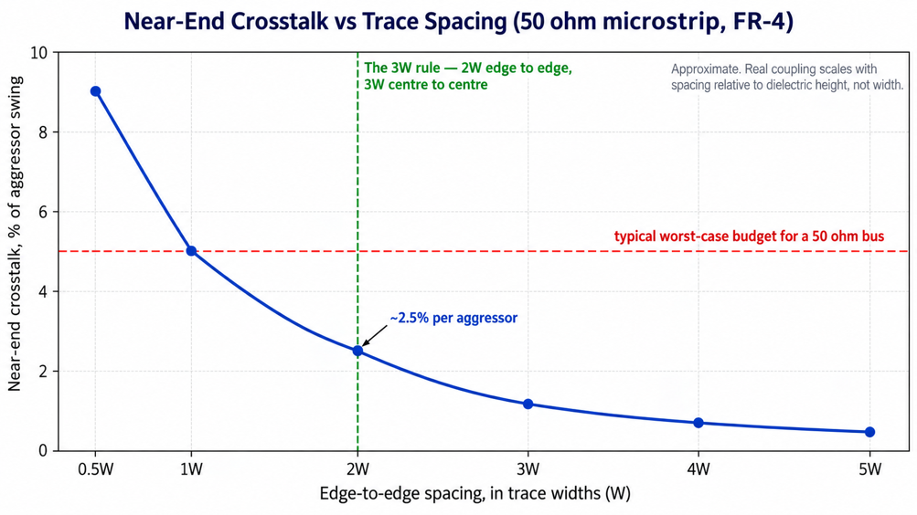
Figure 5: Chart of near-end crosstalk against edge-to-edge spacing in trace widths
Trace width is only standing in for the variable that matters. Coupling is governed primarily by the spacing relative to the dielectric height. Width serves as a proxy because a fixed 50-ohm impedance already determines the width-to-height ratio. Change the impedance target or the plane distance, and the proxy quietly drifts. The more durable habit is keeping every trace close to its reference plane. Shrinking the field is easier than fighting it with spacing. Pulling a signal layer to within 0.1 mm (4 mil) of a plane buys more isolation than another trace width of gap ever will.
| Signal Class | Minimum Edge-to-Edge Gap | Example for a 0.15 mm (6 mil) Trace | What This Buys You |
|---|---|---|---|
| Slow logic below 10 MHz, edges above 5 ns | 1W | 0.15 mm (6 mil) | Coupling stays far below any CMOS noise margin |
| General digital control, SPI, and I2C | 2W | 0.30 mm (12 mil) | The classic 3W rule, worst case near 5% |
| 50 ohm single-ended high-speed nets | 2W, plus a plane within 0.20 mm (8 mil) | 0.30 mm (12 mil) | Roughly 2.5% NEXT per aggressor on FR-4 |
| Differential pair to differential pair | 4W between the nearest traces | 0.60 mm (24 mil) | Keeps pair-to-pair coupling out of the eye budget |
| Clock, reset, or analog beside a switching bus | 5W, or a properly stitched guard | 0.75 mm (30 mil) | Protects the nets where one glitch is fatal |
Controlling Impedance and High-Speed Routing Parameters
Termination reduces how much coupled noise reaches the receiver. An unterminated victim can reflect the noise pulse and make it appear larger.
- Slew rate also matters: A small series resistor, often 22–33 Ω at the driver, slows the edge and reduces far-end crosstalk.
- Differential pairs need consistent spacing: Keep the gap within the pair tight and uniform to maintain impedance, but leave more space between separate pairs to reduce coupling.
- Serpentine routing needs care too: Tight meanders run parallel to themselves and can create extra coupling. Keep the loops well separated—around four trace widths where possible—to preserve clean timing.
From Crosstalk Control to Manufacturable PCB Design
A crosstalk margin that lives only in your head does not survive fabrication. It has to become a design rule, a fabrication note, and a tolerance you already budgeted for.
Turning Signal Integrity Requirements Into Fabrication Rules
Net classes are how spacing intentions become enforceable. A single global clearance rule guarantees the router takes the tightest legal gap everywhere. Give clocks, differential pairs, and analog nets their own classes, each with its own clearance, and let density come from the nets that can afford it.
Fabrication notes carry the half of your design that Gerber's cannot express. A request for a plain 1.6 mm (63 mil) four-layer board leaves every dielectric height to the fab. Spell out what you actually calculated against:
- The full layer order, with each signal layer's intended reference plane named
- The impedance target for every controlled layer, together with its tolerance
- The exact stack-up and prepreg you calculated against, marked as no substitution
- The signal-to-plane height that your spacing rules assumed
- Any net class whose clearance must not be reduced during CAM optimization
Locking the stack-up decides whether your spacing survives. Suppose you designed a 0.1 mm (4 mil) signal-to-plane height, and the panel presses at 0.2 mm (8 mil).
How PCB Manufacturing Accuracy Affects Crosstalk Performance
Etching does not produce the shape your field solver assumed. The etchant attacks sideways as fast as it attacks downward, so a finished trace is trapezoidal with a narrower top. That shifts both the impedance and the effective gap away from nominal.
Width tolerance eats your spacing directly. JLCPCB publishes a track width tolerance of ±20 %, so a 0.10 mm (4 mil) track can finish at 0.12 mm (4.7 mil). Both traces grow toward each other, and a 0.20 mm (7.9 mil) designed gap can arrive at 0.18 mm (7.1 mil).
| Fabrication Variable | JLCPCB Published Tolerance | How It Shifts Coupling | Margin to Design In |
|---|---|---|---|
| Finished track width | ±20%, so 0.10 mm (4 mil) finishes 0.08 to 0.12 mm (3.1 to 4.7 mil) | Wider tracks close the gap from both sides at once | Draw the gap about 10% wider than the solver asked for |
| Controlled impedance | ±10% standard, ±5% on request | Impedance and coupling track the same width and height drift | Check the noise budget at the corner, not at nominal |
| Board and dielectric thickness | ±10% at 1.0 mm (39 mil) and above, ±0.1 mm (4 mil) below | A thicker press lifts the trace away from its plane | Do not spend the last 10% of your spacing-to-height ratio |
| Prepreg dielectric constant | Published per glass style, 3.91 for 1080 up to 4.4 for 7628 | Dk changes how the field splits between traces and plane | Calculate against the fab stack-up, not a generic 4.5 |
| Layer-to-layer registration | Held by tooling, and never exactly zero | Shifts a stripline off center, so one plane sits closer | Treat stripline symmetry as approximate, not exact |
How Professional PCB Manufacturers Support Crosstalk-Sensitive Designs
No fab measures crosstalk on your board, since coupling belongs to your layout rather than to their process.
Engineering Review, DFM, and Impedance Control
Automated DFM analysis is the first filter. It compares your clearances against process minimums and flags anything the etching line cannot resolve. That matters because a carefully specified 3W gap is worthless if the router squeezes it below the manufacturable limit inside a fanout.
In controlled impedance, crosstalk work becomes an order parameter. It is available from four layers upward, with plus or minus 10% tolerance, or plus or minus 5% on request. The free calculator returns the trace width and the qualifying stack-ups, built from real pressed thicknesses and per-prepreg Dk values. Once you have picked one, you can send your stack-up straight to production.
Manufacturing Inspection and Electrical Verification
Automated optical inspection is the check that protects your spacing. Cameras compare the etched copper against your Gerber data. They flag traces that came out narrow, gaps that came out tight, and any nick in a conductor edge, so the gaps you drew get verified before the panel moves on.
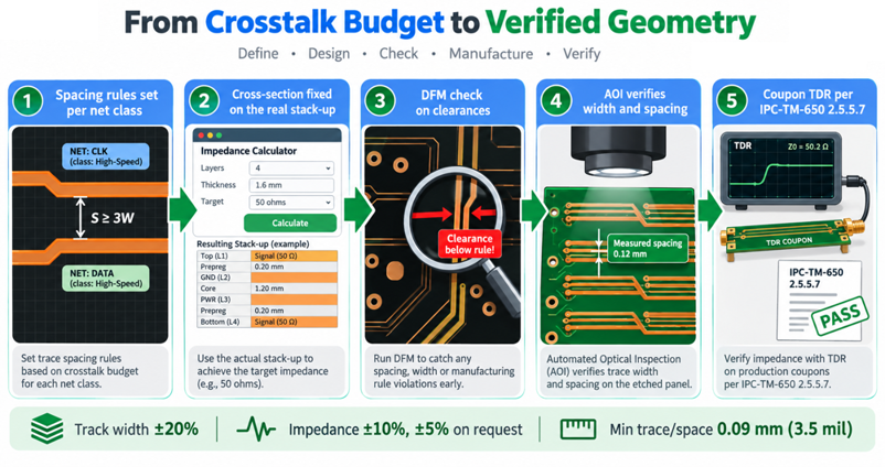
Figure 6: How fabrication tolerances feed back into a crosstalk-safe stack-up
Electrical test proves something different from what people assume. Flying probe and fixture testing confirm that every net is continuous and that no two nets are shorted. Neither says anything about how strongly two isolated nets couple, so passing the electrical test is not evidence that your crosstalk budget holds.
FAQ About PCB Crosstalk
Q: What is the difference between NEXT and FEXT in a PCB?
Near-end crosstalk appears at the driver end of the victim trace. It stops growing once the parallel run exceeds about half the physical length of the rise time. Far-end crosstalk appears at the receiver end and grows with coupled length. It is almost absent on inner stripline layers, because the surrounding dielectric is uniform.
Q: Does JLCPCB provide a PCB crosstalk calculator?
No. JLCPCB publishes an impedance calculator and a PI stiffener calculator, but not a crosstalk tool. Use the impedance calculator to fix your real trace width and dielectric height first. Then feed those dimensions into your EDA suite's field solver or a third-party crosstalk estimator.
Q: Is a guard trace better than simply increasing trace spacing?
Usually not on outer layers. A guard trace only helps when vias stitch it to the reference plane at close intervals, well under a quarter wavelength of the highest frequency present. An unstitched guard can carry energy from the aggressor to the victim and make things worse. Spending the same board width on plain separation is often more reliable.
Q: Does widening my traces reduce PCB crosstalk?
Not by itself, because coupling is governed by the gap between traces measured against the height to the reference plane. Widening a trace at a fixed routing pitch actually shrinks the gap. Lowering the trace closer to its plane, or opening the gap, is what reduces crosstalk.
Conclusion
Crosstalk is not a defect that appears in your board. It is a consequence of geometry that existed from the first trace you routed. The aggressor's changing fields couple into whatever sits inside them, so the only questions are how much, at which end, and whether the receiver can absorb it.
- Near-end crosstalk (NEXT): Saturates with length, so the main controls are greater trace spacing and a closer reference plane.
- Far-end crosstalk (FEXT): Increases with parallel length on microstrip, is greatly reduced in stripline, and decreases when edge rates are slowed.
NEXT and FEXT respond differently, so each needs a different routing strategy.
Edge rates keep getting faster while supply voltages keep falling, so the margin available to absorb coupled noise thins with every generation. JLCPCB's free impedance calculator, published stack-ups, and coupon TDR reports make that loop cheap enough to run on every revision.

Popular Articles
Keep Learning
Stop PCB Crosstalk Before It Becomes a Signal Integrity Problem
Key Takeaways NEXT vs FEXT: NEXT saturates with trace length, while FEXT grows linearly with distance. Spacing & Stackup: Apply the 3W rule and keep traces close to reference planes. Edge Rates: Fast rise times drive crosstalk more than clock frequency. Fab Margins: Etching variations reduce gaps, requiring extra layout clearance. Verification: Use DFM checks and TDR coupons instead of basic continuity tests. PCB crosstalk is the noise one trace pushes into its neighbor, even though the two nets are e......
Navigating the Impedance Landscape: Selecting the Right Impedance for USB, Ethernet, HDMI, and SD Card Interfaces
Introduction In the realm of high-speed digital communication, choosing the right impedance is a critical aspect of successful PCB design. Impedance matching ensures optimal signal integrity, minimizes reflections, and enhances the overall performance of interfaces such as USB, Ethernet, HDMI, and SD Card. In this blog post, we'll explore the importance of impedance, the factors influencing impedance selection, and best practices for ensuring reliable data transmission in these widely used interfaces.......
A Beginners Guide to Impedance Control in PCBs
When a digital signal is transmitted from one point to another, it causes a change in the state of the signal line. This change can be understood as an electromagnetic wave moving through the circuit. Reflection occurs when this wave encounters a boundary between different mediums. At this boundary, some of the wave's energy continues as a signal, while the rest is reflected. This process repeats until the energy is either absorbed by the circuit or dissipated into the environment. For electrical engi......
What is PCB Signal Attenuation: How Signals Weaken Over Distance and How to Mitigate It
Key Takeaways Primary Causes: Signal attenuation is mainly caused by skin effect (conductor loss) and substrate energy absorption (dielectric loss). How to Mitigate: Reduce loss by using wider traces, low-loss materials, controlled impedance, and removing via stubs. JLCPCB Solutions: JLCPCB offers Rogers high-frequency laminates, High-TG FR4, precision impedance control, and backdrilling to protect signal integrity. As a signal travels from the source to the load through PCB conductors, the signal is ......
Understanding Analog and Digital Ground in PCB Design
When working on printed circuit board (PCB) design, proper grounding is crucial for ensuring signal integrity, minimizing noise, and maintaining reliable performance. Two common types of ground planes used in PCB layouts are Analog and Digital ground. In this article, we will explore the differences between analog and digital ground, their significance in PCB design, and best practices for their implementation. Analog Ground vs. Digital Ground Analog ground and digital ground have separate purposes in......
Design Guide for USB-3.0 Differential Signaling
In the world of data transfer, USB 3.0 is the Usain Bolt to USB 2.0’s friendly jogger. USB 2.0 is called “High Speed” and limped along at 480 Mb/s, whereas USB 3.0 SuperSpeed rockets up to 5 Gb/s (over ten times faster). But this speed jump brings full‑duplex operation and new differential transmit (SSTX) and receive (SSRX) pairs on dedicated pins. USB 2.0 D+/D– lines handle enumeration and legacy data, while two new 5 Gb/s high‑speed differential pairs carry SuperSpeed data in each direction. While m......