
BJT vs MOSFET: Differences, Advantages, Applications and When to Use Each
22 min
- What is the Difference Between BJT and MOSFET?
- When to Use BJT vs MOSFET (Quick Answer)
- BJT vs MOSFET: Key Differences Explained
- How to Choose Between BJT and MOSFET (Practical Guide)
- What Is a BJT (Bipolar Junction Transistor)?
- What Is a MOSFET?
- How Does a BJT Work?
- How Does a MOSFET Work?
- Advantages of BJT
- Disadvantages of BJT
- Advantages of MOSFET
- Disadvantages of MOSFET
- BJT vs MOSFET in Switching Applications
- BJT vs MOSFET in Amplifier Circuits
- BJT vs MOSFET in SMD Packages (SOT-23, SOT-223, DPAK)
- BJT vs MOSFET in PCB Design and Assembly
- BJT and MOSFET in Real Applications
- Common Mistakes When Choosing MOSFET or BJT
- Conclusion: BJT vs MOSFET: Which Should You Choose?
- FAQ about BJT vs MOSFET
In modern electronics, choosing between a BJT and MOSFET directly impacts switching speed, power efficiency, and PCB layout - especially in SMD designs. While BJTs are current-controlled devices ideal for analog circuits, MOSFETs are voltage-controlled and dominate high-speed switching applications.
In this guide, we compare BJT vs MOSFET in terms of switching speed, SMD packaging, thermal performance, and real-world PCB applications to help you choose the right component.
What is the Difference Between BJT and MOSFET?
The main difference between a Bipolar Transistor vs MOSFET is that a BJT is a current-controlled device, while a MOSFET is voltage-controlled. This makes MOSFETs faster and more efficient for switching applications, while BJTs are better suited for analog amplification where linearity and low noise matter more than switching speed.
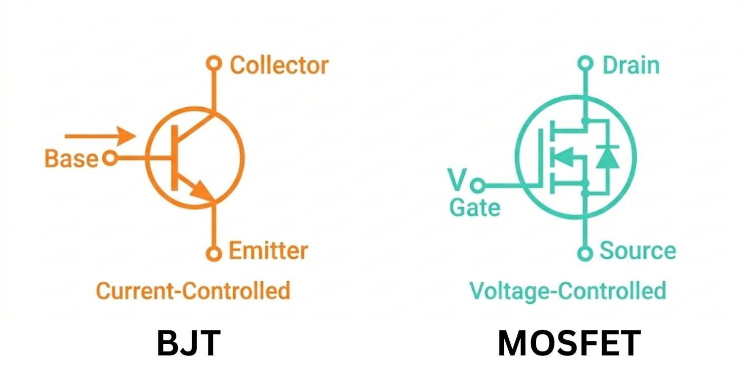
Figure: BJT vs MOSFET showing NPN transistor current-controlled symbol versus N-channel MOSFET voltage-controlled symbol
When to Use BJT vs MOSFET (Quick Answer)
- Use MOSFET → switching, MCU control, PWM, power circuits
- Use BJT → analog amplification, audio, RF, current mirrors
- Not sure? → MOSFET is the safer default in modern SMD PCB design
BJT vs MOSFET: Key Differences Explained
| Feature | BJT | MOSFET |
|---|---|---|
| Control | Base current (IB) | Gate voltage (VGS) |
| Switching speed | Slower (10-100 ns) | Faster (1-10 ns small-signal; 10s of ns for power devices) |
| Input impedance | Low (~kΩ) | High (~MΩ) |
| On-state drop | VCE(sat) ≈ 0.1-0.3V | V = I × RDS(on) (<10mΩ possible) |
| Body diode | None | Present (intrinsic) |
| EMI / dv/dt | Lower - easier on EMI | Higher - needs filtering |
| Best use | Analog, audio, RF | Switching, power, digital |
MOSFET vs BJT Transistor: Key Differences Summary
- BJT uses base current (IB) to control collector output - current in, current out
- MOSFET uses gate voltage (VGS) to open or close a conduction channel - voltage in, no steady current
- BJT draws continuous input current while conducting - adds drive circuit power cost
- MOSFET has near-zero steady-state gate current - only charges/discharges gate capacitance during transitions
- MOSFET has an intrinsic body diode (PN junction between source and body); BJT has none
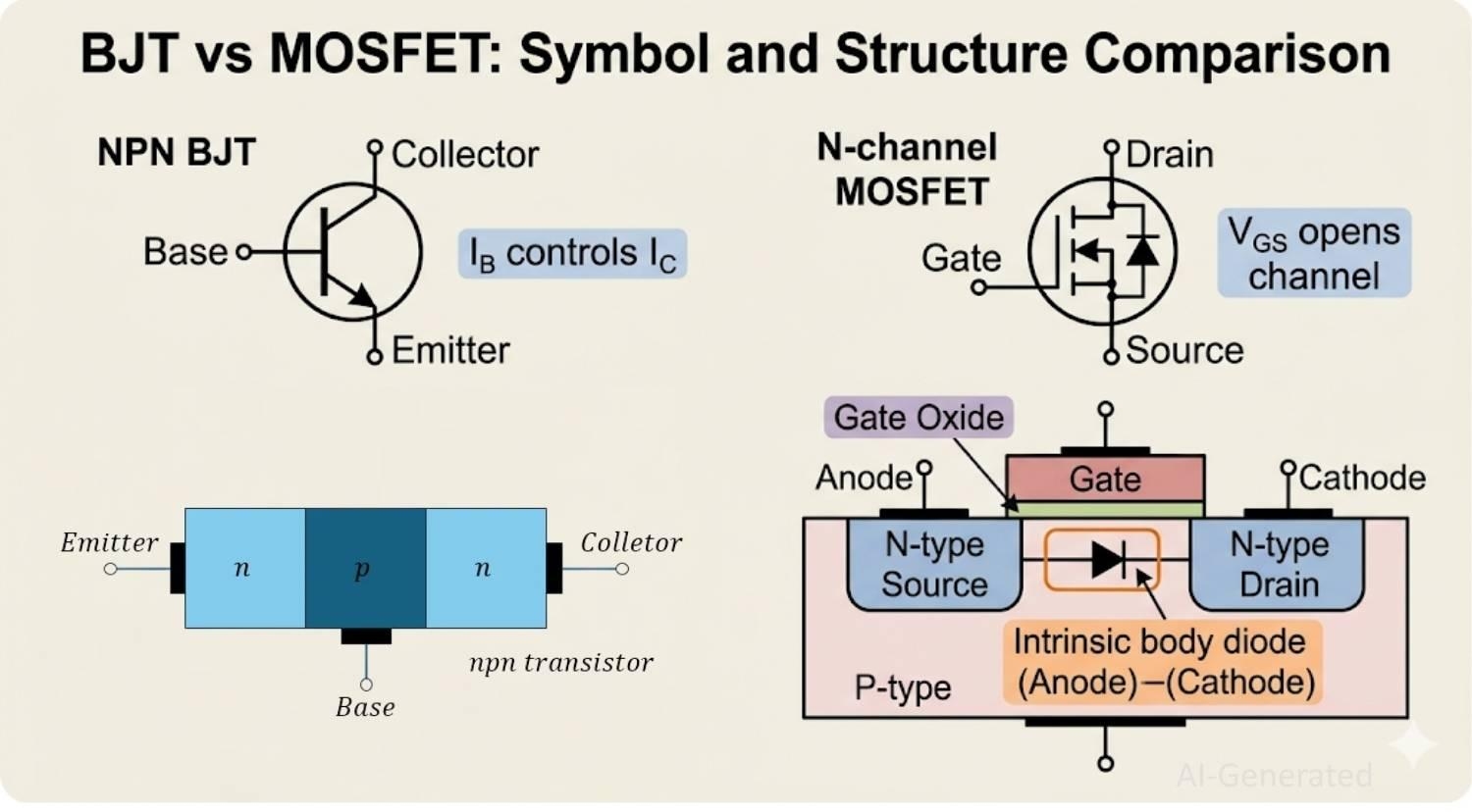
Figure: BJT vs MOSFET schematic symbols and semiconductor structure comparison showing NPN transistor base-emitter-collector and N-channel MOSFET gate-source-drain with body diode
How to Choose Between BJT and MOSFET (Practical Guide)
Follow this decision logic to eliminate ambiguity in most PCB design scenarios.
Is the application ANALOG (amplifier, audio, RF)?
→ YES → Use BJT
→ NO ↓
Is it a DIGITAL SWITCH or POWER STAGE (>10 kHz)?
→ YES → Use logic-level MOSFET
→ NO ↓
Voltage > 200V at LOW power (<500mW)?
→ YES → BJT may be more cost-effective
→ NO → Use MOSFET (verify Vth for your drive voltage)
Driving from a 3.3V MCU GPIO?
→ YES → Logic-level MOSFET (Vth < 2V, full enhancement at 3.3V)
→ NO → Standard MOSFET or BJT per above
What Is a BJT (Bipolar Junction Transistor)?
A BJT (Bipolar Junction Transistor) is a three-terminal semiconductor device with a Base (B), Collector (C), and Emitter (E). It comes in two polarities: NPN (most common) and PNP. The name "bipolar" refers to the fact that both electrons and holes participate in current conduction - unlike MOSFETs, which rely on a single carrier type.
BJTs are available in small-signal variants (e.g., MMBT3904, BC817) for amplification and switching at low currents, and in power variants (e.g., TIP31, MJE13003) for higher-current applications. In SMD designs, SOT-23 and SOT-89 cover the vast majority of BJT use cases.
What Is a MOSFET?
A MOSFET (Metal-Oxide-Semiconductor Field-Effect Transistor) is a three-terminal device with a Gate (G), Drain (D), and Source (S). It comes in N-channel and P-channel types, and within those, enhancement mode (normally off - the standard for switching) and depletion mode (normally on - less common). An intrinsic body diode between source and drain is a structural feature of all MOSFETs.
MOSFETs dominate modern switching design because the gate draws no DC current, enabling direct interface with microcontroller outputs. In SMD form, they range from compact SOT-23 logic-level devices (e.g., 2N7002, IRLML2502) to high-current power packages like DPAK and SO-8.
How Does a BJT Work?
BJT Working Principle
A BJT operates by using a small base current (I_B) to control a much larger collector current (IC). The relationship between the two is the DC current gain: β (hFE) = IC / IB, typically 50–300 for small-signal devices.
When a sufficient forward voltage is applied to the base-emitter junction (VBE ≈ 0.6-0.7V for silicon), the device enters the active region - collector current flows proportionally to base current. This is the basis of BJT amplification. When driven into saturation (both junctions forward-biased), the transistor acts as a closed switch with a low VCE(sat) of ~0.1-0.3V. When the base drive is removed, the device enters cutoff, and no collector current flows.
The key limitation for switching: charge stored in the base region during saturation must be swept out before the device turns off, creating a storage time (ts) that limits switching speed to the 10-100 ns range.
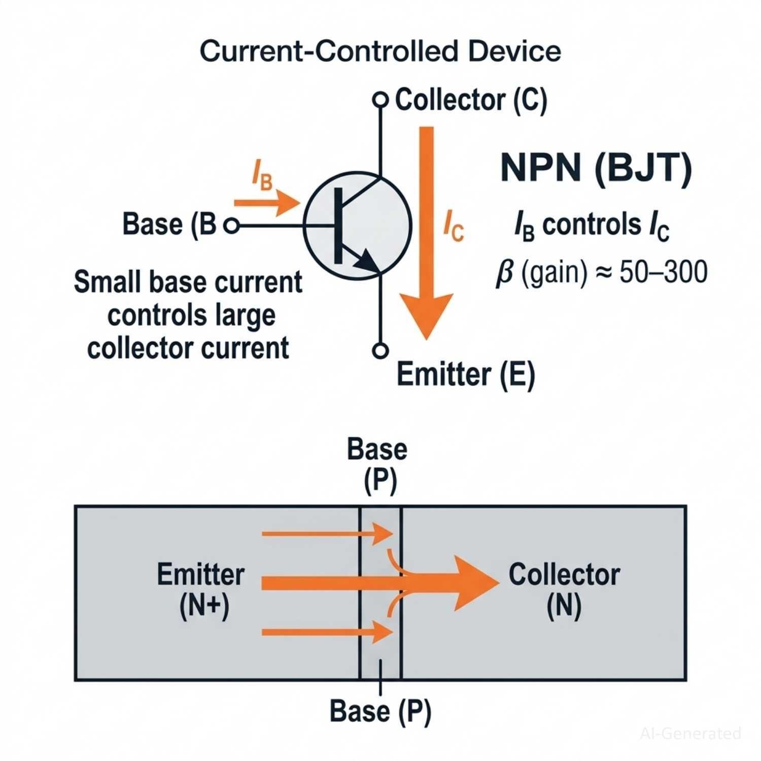
Figure: BJT working principle diagram showing NPN transistor with base, collector, and emitter, illustrating how small base current controls large collector current through semiconductor layers
How Does a MOSFET Work?
MOSFET Working Principle
A MOSFET operates by applying a voltage between Gate and Source (VGS) to create or deplete a conduction channel between Drain and Source. No current flows into the gate in steady state - the gate is isolated from the channel by a thin layer of silicon dioxide (gate oxide), giving it near-infinite DC input impedance.
When VGS exceeds the threshold voltage (Vth), the channel forms and current can flow from Drain to Source. The device resistance in this on-state is characterized by RDS(on) - modern low-voltage MOSFETs can achieve RDS(on) below 10mΩ. When VGS drops below V_th, the channel disappears, and the device turns off with no charge storage delay, enabling nanosecond-range switching transitions.
The body diode, formed by the PN junction between the body (substrate) and drain, conducts in the reverse direction regardless of gate state - a design consideration in H-bridges, synchronous rectifiers, and any topology with bidirectional current paths.
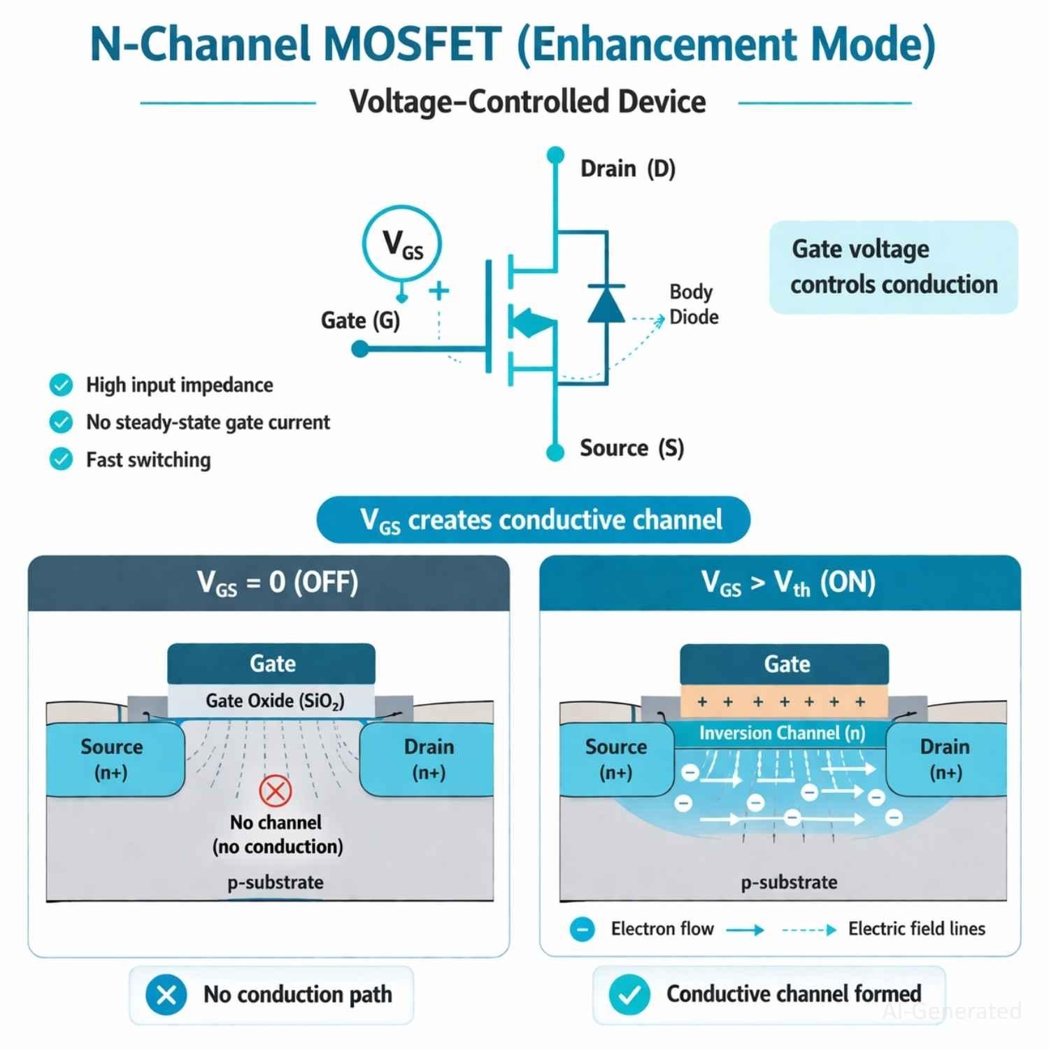
Figure: MOSFET working principle diagram showing an N-channel enhancement mode transistor with gate, source, and drain, illustrating channel formation when gate voltage VGS exceeds threshold
Advantages of BJT
- High DC current gain (β = 50-300) makes signal amplification straightforward
- More linear I-V relationship - preferred in Class A/AB audio amplifiers
- No gate oxide - more robust against ESD than MOSFETs (though not completely immune)
- Lower cost at high voltages (>200V), where MOSFET process complexity adds cost
- Lower 1/f noise in certain analog and RF applications (MOSFETs may outperform in high-frequency or CMOS-based designs)
- No body diode - avoids unintended reverse conduction
Disadvantages of BJT
- Requires continuous base current while on - adds drive circuit power consumption
- Slower switching (10-100 ns) due to minority carrier storage time (ts)
- More complex biasing for linear applications (VBE stabilization needed)
- Lower input impedance (~kΩ) - harder to drive from high-impedance sources
Advantages of MOSFET
- Voltage-controlled with near-zero DC gate current - simple logic interfacing; note that fast switching at high frequency still requires significant transient gate drive current due to gate capacitance
- Much faster switching - typically 1-10 ns for small-signal devices; power MOSFETs may be in the tens of nanoseconds range depending on Qg and driver strength
- Very low RDS(on) (<10mΩ) in modern devices - minimal conduction loss at high current
- High input impedance (~MΩ) - compatible with direct MCU GPIO driving
- Body diode provides freewheeling in inductive load applications
Disadvantages of MOSFET
- Gate oxide is sensitive to ESD - requires handling precautions and PCB protection
- Higher dv/dt during switching - can range from a few V/ns to tens of V/ns depending on gate drive and circuit conditions, increasing EMI
- Gate capacitance (Ciss = 100pF-nF range) requires a strong driver for high-frequency operation
- A body diode can cause unwanted reverse conduction in some topologies
- Higher cost in high-voltage (>200V) designs compared to BJTs
BJT vs MOSFET in Switching Applications
Switching Speed of BJT vs MOSFET
Switching speed is the biggest performance difference between BJTs and MOSFETs in modern PCB design.
Key Takeaway:
- MOSFET: typically 1-10 ns for small-signal devices; power MOSFETs often 10s of ns depending on gate charge
- BJT: 10-100 ns switching → limited by minority carrier storage time (ts)
- Above ~50 kHz → MOSFET is almost always required for acceptable efficiency
MOSFETs can switch in the nanosecond range - typically 1-10 ns for small-signal devices, but often tens of nanoseconds for power MOSFETs, depending on gate charge (Qg) and driver strength. BJTs typically take 10-100 ns because of minority carrier storage: when a BJT saturates, charge builds up in the base region and must be physically swept out before the device can turn off. This storage time (ts) directly limits maximum switching frequency.
Power Loss of BJT vs MOSFET
For DC-DC converters, gate drivers, or any design running above ~50 kHz, that difference translates directly into switching losses:

At 500 kHz with identical load conditions, a MOSFET can produce 5-10× lower switching losses than a comparable BJT. However, faster switching produces steeper dv/dt edges - which can range from a few V/ns to tens of V/ns depending on gate drive and circuit conditions - radiating more EMI and stressing adjacent traces. BJTs' slower di/dt is actually a design advantage in some industrial or motor-drive contexts where EMI filtering costs more than efficiency gains.
In practice, engineers add gate resistors (10-47Ω) to slow edges and tame EMI without sacrificing much efficiency. While MOSFETs require no steady-state gate current, fast switching at high frequency still demands significant transient current from the gate driver due to gate capacitance - a MOSFET gate (Ciss = 100pF to several nF for power devices) cannot be driven fast from a logic pin alone at frequencies above a few hundred kHz. BJT base networks are simpler at low frequencies but become inefficient above ~100 kHz.
For SMT assembly, the SMD reflow soldering process for PCB assembly handles both device types equally - the real design work is in the drive circuit and layout, not the soldering.
Thermal Performance of BJT vs MOSFET
Switching losses and conduction losses both contribute to junction temperature, and the two devices generate heat in fundamentally different ways.
BJT conduction loss is determined by VCE(sat) × IC. At light loads, this is predictable and relatively low - a BJT saturated at 200mA with VCE(sat) of 0.2V dissipates only 40mW. However, at higher currents or frequencies, the slower switching transitions add significant dynamic loss on top of static conduction loss.
MOSFET conduction loss is governed by I² × RDS(on). At low currents, this is negligible - a 10mΩ MOSFET carrying 1A dissipates just 10mW. At higher currents, the I² relationship becomes significant, which is why selecting the lowest practical RDS(on) matters for power stages. The advantage is that dynamic (switching) losses remain low thanks to fast transitions.
In both cases, SMD packages dissipate heat through PCB copper - there is no external heatsink. A larger drain or collector pad, combined with thermal vias on multilayer boards, is the primary tool for keeping junction temperatures within spec.
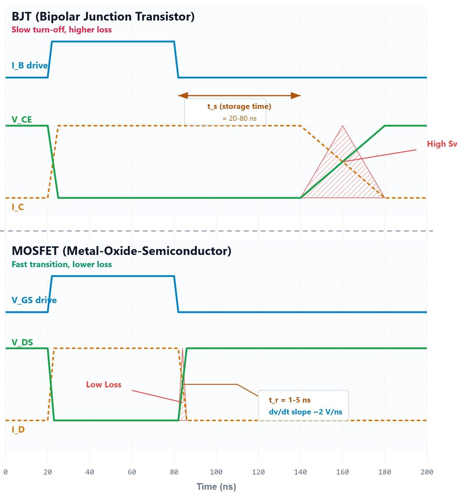
Figure: BJT vs MOSFET switching waveform comparison showing BJT storage time delay of 20 to 80 nanoseconds versus MOSFET fast 1 to 5 nanosecond switching transition with dv/dt annotation
BJT vs MOSFET in Amplifier Circuits
When designing amplifier circuits, the choice between BJT and MOSFET depends on gain behavior, linearity, and noise characteristics. While both devices can operate in linear regions, BJTs are generally preferred for small-signal analog amplification, whereas MOSFETs are more common in power or switching-oriented designs.
Gain Characteristics
BJTs offer higher transconductance (gₘ) for a given current compared to MOSFETs. Since BJT collector current is exponentially related to base-emitter voltage, even small input changes produce significant output variation.
- BJT: Higher gain at low currents → ideal for small-signal amplification
- MOSFET: Lower intrinsic gain → often requires additional stages
In practical terms, a BJT amplifier can achieve higher voltage gain with simpler circuit design, especially in low-power analog applications.
Linearity
Linearity determines how accurately an amplifier reproduces the input signal without distortion.
- BJT: More linear in active region due to exponential I-V behavior
- MOSFET: Less linear, especially near the threshold region
BJTs are widely used in Class A and Class AB amplifiers because they maintain better linearity over a wide operating range. MOSFETs, while usable in linear mode, often introduce more distortion unless carefully biased.
Noise Performance
Noise is critical in sensitive analog and RF circuits.
- BJT: Lower 1/f (flicker) noise → better for low-frequency and precision analog
- MOSFET: Higher flicker noise but better in some high-frequency CMOS designs
For applications like:
- microphone preamplifiers
- RF front-end stages
- sensor signal conditioning
BJTs are typically the preferred choice due to their superior low-noise performance.
BJT vs MOSFET in SMD Packages (SOT-23, SOT-223, DPAK)
Package selection is where electrical performance meets physical PCB constraints - and where many design errors begin.
| Package | Typical PD | Common Use |
|---|---|---|
| SOT-23 (3-pin) | 150-300 mW | Signal switching, logic interfaces |
| SOT-89 | 500 mW-1W | Small power stages |
| SOT-223 | 1-2W | Medium power with PCB heat spreading |
| DPAK (TO-252) | 2-3W | Motor drive, power rails |
| D2PAK (TO-263) | 3-5W | High-current SMD power stages |
| PowerSO-8 / SO-8 | Up to 5W+ | H-bridges, synchronous rectifiers |
Watch out for SOT-23 pinout differences - this is one of the most common PCB spin causes. For an NPN BJT (e.g., MMBT3904): pin 1 = Base, pin 2 = Emitter, pin 3 = Collector.
For an N-channel MOSFET (e.g., 2N7002): pin 1 = Gate, pin 2 = Source, pin 3 = Drain.
The packages look identical on a reel. Always verify against the component datasheet - not generic pinout diagrams. Understanding how to identify SMD transistors and their codes is essential before placing an order.
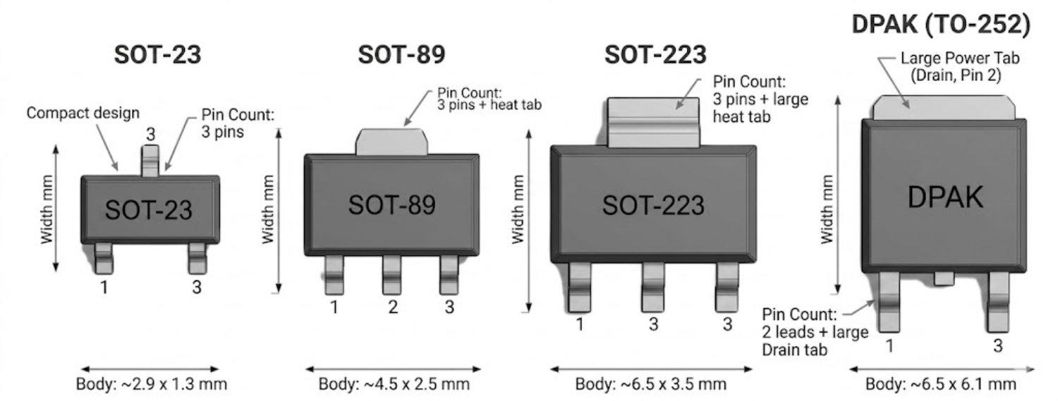
Figure: SMD transistor package size comparison showing SOT-23, SOT-89, SOT-223, and DPAK.
Common SMD part numbers:
Small-signal BJTs (SOT-23):
- MMBT3904 - NPN, 40V, 200mA, β ≈ 100-300
- MMBT3906 - PNP complement to MMBT3904
- BC817-40 - NPN, 45V, 500mA, high-gain variant
Logic-level MOSFETs (SOT-23):
- 2N7002 - N-channel, 60V, 115mA, Vth ~1-2.5V
- IRLML2502 - N-channel, 20V, 3A, RDS(on) 45mΩ @ 4.5V
- FDN306P - P-channel, 30V, 2.5A
Power MOSFETs (SOT-223 / DPAK / SO-8):
- IRF7301 - Dual N-channel, 40V, 14A, SO-8
- STN6NF06 - N-channel, 60V, 32A, PowerSO-8
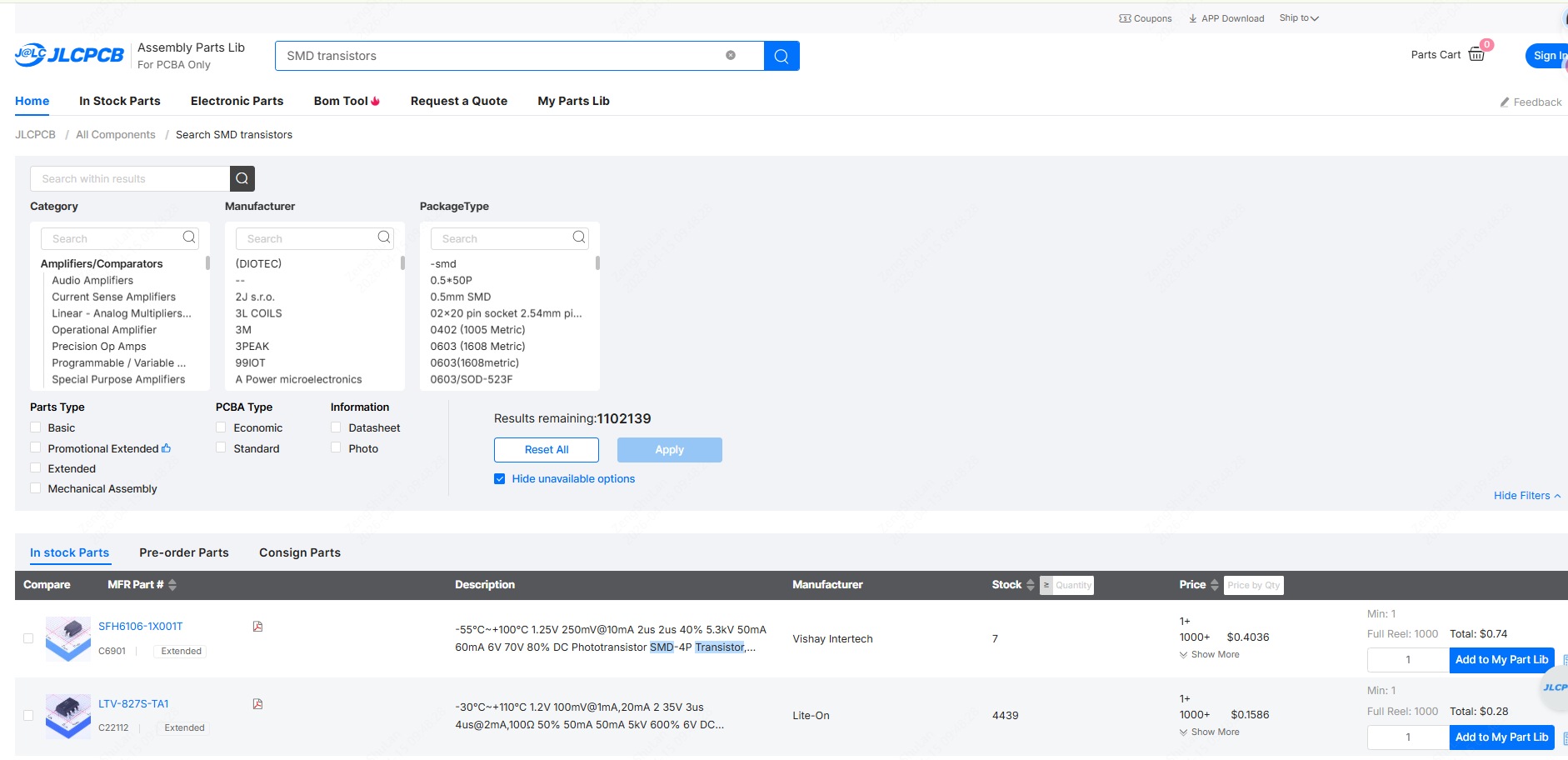
Browse available SMD transistors in the JLCPCB parts library for turnkey BOM sourcing.
BJT vs MOSFET in PCB Design and Assembly
Your BJT vs MOSFET selection doesn't just affect circuit performance - it directly shapes how your PCB is laid out, assembled, and sourced.
Impact of BJT vs MOSFET Selection on PCB Design
The device you choose determines several downstream PCB design decisions that are easy to underestimate early in a project.
# Footprint and pad design: Both BJTs and MOSFETs are available in identical SMD packages (SOT-23, SOT-89, SOT-223, DPAK), but their pin assignments differ. A SOT-23 NPN BJT (MMBT3904) has Base on pin 1, Emitter on pin 2, Collector on pin 3. A SOT-23 N-channel MOSFET (2N7002) has Gate on pin 1, Source on pin 2, and Drain on pin 3. Using the wrong footprint is one of the most common causes of a PCB spin. Always use NSMD (non-solder-mask-defined) pads per IPC-7351 for stronger solder joints and better thermal contact - the solder pad design guide covers this in detail.
# Thermal design: In SMD, there is no external heatsink - PCB copper is the heatsink. For BJTs, conduction loss is VCE(sat) × IC; for MOSFETs, it is I² × RDS(on). Both require adequate copper area on the drain or collector pad to dissipate heat. For power packages (SOT-223, DPAK), use a copper pour of at least 1cm² and add a grid of thermal vias (0.3mm drill, 1mm pitch) on multilayer boards to conduct heat to inner layers or the bottom ground plane. For large exposed pads, apply solder paste at ~60-80% area coverage using a segmented aperture to prevent voiding.
# Power routing: MOSFETs typically handle higher switched currents than comparable BJTs in the same package. Power traces to the drain and source pads should be sized for the full load current - a minimum of 1mm trace width per amp as a starting rule, wider with copper pours for high-current stages. For BJTs in linear or amplifier applications, base resistor and biasing network placement affects noise and stability; keep base leads short and away from high-current paths.
# Gate and base drive layout: MOSFETs require a low-impedance gate drive path - keep the gate resistor close to the device and the drive loop area small to minimize parasitic inductance. For BJTs, the base resistor sets the drive current; place it directly between the drive source and the base pin with no long traces.
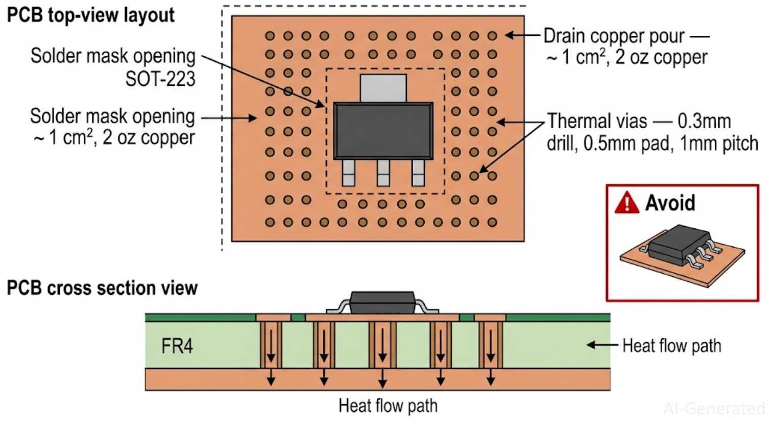
Figure: SMD MOSFET PCB thermal layout showing SOT-223 package with drain copper pour and thermal vias connecting top layer to bottom ground plane for PCB heat dissipation
Component Sourcing and Availability
Standard packages with broad supply: Both BJTs and MOSFETs in SOT-23, SOT-223, and DPAK are among the most widely stocked SMD components in the industry. General-purpose parts like the MMBT3904 (NPN BJT) and 2N7002 (N-channel MOSFET) are available from dozens of distributors and are rarely subject to supply disruptions.
Sourcing stability: For cost-sensitive or high-volume designs, BJTs in standard packages (SOT-23, SOT-89) are often the most stable in terms of cross-vendor availability - multiple manufacturers produce pin-compatible versions. Logic-level MOSFETs have slightly more variation in Vth and RDS(on) between manufacturers, so component verification against the specific datasheet is important when qualifying an alternate source.
Part interchangeability: Many BJT types (e.g., MMBT3904/MMBT3906) have direct equivalents across Nexperia, ON Semiconductor, Diodes Inc., and others with identical specs and footprints. MOSFET equivalents exist but require careful verification of Vth, RDS(on) vs VGS curves, and gate charge (Qg) before substitution - these parameters vary more between vendors than BJT β.
BOM planning: For designs going to SMT assembly, confirm component stock before finalizing your BOM. Short lead times on standard transistor packages make last-minute substitutions rare, but specialty parts (e.g., dual MOSFETs in SO-8, high-voltage BJTs in SOT-223) can have longer lead times.
Reliable PCB Assembly with JLCPCB
Getting MOSFET vs BJT transistor selection right on paper only matters if the SMT assembly process executes it correctly. Key manufacturing reliability factors include:
Component verification: Before SMT assembly begins, each component is verified against the BOM - part number, package, and orientation. For SOT-23 devices especially, correct BJT vs MOSFET orientation and pin mapping is confirmed against the pick-and-place file to prevent placement errors that wouldn't be caught until functional test.
Quality control: Assembled boards go through automated optical inspection (AOI) and, for power transistor pads, X-ray inspection can identify solder voiding on thermal pads - voids increase thermal resistance and can cause devices to run hotter than expected in the field.
BJT vs MOSFET selection support: JLCPCB's parts library includes thousands of stocked BJTs and MOSFETs across SOT-23, SOT-89, SOT-223, DPAK, and SO-8 packages, with real-time stock visibility. This means your BJT vs MOSFET selection can be validated against actual available inventory before the board is fabricated, reducing the risk of last-minute BOM changes.
Manufacturing reliability: JLCPCB's PCB assembly service uses controlled SMT reflow profiles matched to component thermal specifications - critical for power MOSFETs and BJTs in exposed-pad packages where solder joint quality directly affects thermal performance. Browse components and confirm availability at the JLCPCB parts library before submitting your design.
BJT and MOSFET in Real Applications
Real circuit examples clarify which device performs better where performance actually matters.
| Application | Better Choice | Reason |
|---|---|---|
| Audio amplifier (Class A/AB) | BJT | Linear I-V, low noise, stable V_BE |
| DC motor driver (PWM) | MOSFET | Fast switching, low RDS(on) |
| LED dimmer (digital PWM) | MOSFET | Direct MCU drive, efficient |
| LED dimmer (analog/linear) | BJT | Better linearity, lower noise |
| Buck / boost converter | MOSFET | Sub-ns switching, low Esw |
| H-bridge (robotics) | MOSFET | Body diode handles freewheeling |
| Current mirror | BJT | VBE matching, linear behavior |
| Load switch (3.3V rail) | Logic-level MOSFET | Direct GPIO drive, near-zero input current |
| High-voltage (>300V) low-power | BJT | Lower cost, simpler process |
| RF small-signal amplifier | BJT (or SiGe) | Low noise, better linearity |
Common Mistakes When Choosing MOSFET or BJT
These errors cause the majority of transistor-related PCB respins - and all of them are avoidable.
#1. Using a non-logic-level MOSFET with a 3.3V MCU:
Many MOSFETs require VGS of 4.5-10V to reach rated RDS(on). At 3.3V, they may sit partially on and dissipate excess heat. Always check the RDS(on) vs VGS curve - look for "logic-level" types with full enhancement at VGS = 2.5-3.3V.
#2. Ignoring SOT-23 pinout differences
BJT and MOSFET SOT-23 packages have different pin assignments. Installing a MOSFET in a BJT footprint gives a non-functional or damaged circuit. Always reference the component datasheet - never a generic pinout diagram.
#3. Insufficient thermal copper on power packages
A DPAK or SOT-223 on minimal copper without thermal vias limits the device to a fraction of its rated power. A 2W device on a 5mm × 5mm copper pour runs significantly hotter than the same device on a 20mm × 20mm pour with via grid. Size the pour first - don't leave it to the autorouter.
#4. Forgetting the MOSFET body diode
In synchronous rectifier or H-bridge designs, the body diode conducts during dead time, generating heat and reducing efficiency. A parallel Schottky diode with faster reverse recovery is often needed alongside the MOSFET.
#5. Choosing BJT for a 500 kHz converter
At that frequency, BJT switching losses and storage time are prohibitive. MOSFET switching losses at 500 kHz remain manageable with proper gate drive - BJT losses at the same frequency can be 5-10× higher.
#6. Skipping ESD protection on MOSFET gates
Gate oxide can fail from static discharge during handling or from inductive spikes on the PCB. A 100kΩ gate pull-down resistor and an optional TVS diode between gate and source are cheap insurance.
Conclusion: BJT vs MOSFET: Which Should You Choose?
For switching, PWM, and MCU-driven circuits, MOSFETs are the clear winner - faster switching, lower losses, and direct logic interfacing make them the default choice in modern SMD PCB design. For analog amplification and precision circuits, BJTs remain the better choice due to their linearity, noise characteristics, and ESD robustness.
FAQ about BJT vs MOSFET
Q: What is the main difference between BJT and MOSFET?
A BJT is controlled by base current; a MOSFET is controlled by gate voltage. This makes MOSFETs easier to drive from logic circuits, faster switching, and more efficient in switching applications. BJTs offer better linearity and lower noise in analog circuits.
Q: What is the difference between MOSFET and a transistor?
"Transistor" covers both BJTs and MOSFETs. In common usage, "transistor" often refers to a BJT. MOSFETs are technically also transistors - field-effect transistors - controlled by voltage rather than current.
Q: Are BJTs outdated compared to MOSFETs?
No. BJTs remain widely used in audio amplifiers, RF circuits, current mirrors, and high-voltage power supplies. MOSFETs have displaced them in high-frequency power switching, but BJTs remain the right choice for many analog applications.
Q: MOSFET vs BJT - which is better for switching?
MOSFETs are better for switching in nearly all modern applications. They switch faster - typically 1-10 ns for small-signal devices (power MOSFETs may be slower depending on gate charge) - have lower switching losses, and require no DC drive current. Logic-level MOSFETs switch directly from 3.3V MCU outputs without additional circuitry.
Q: MOSFET vs BJT - which is better for an amplifier?
BJTs are generally better for analog amplifiers. Their more linear I-V response, predictable VBE (~0.6V), and lower 1/f noise make them preferred in audio, RF, and precision analog stages.
Q: How does SMD packaging affect thermal performance for MOSFETs vs BJTs?
In SMD designs, PCB copper is the primary heatsink. Larger drain or collector pad areas dissipate more heat. For power packages (SOT-223, DPAK), thermal vias on multilayer boards are essential to move heat away from the junction and prevent thermal shutdown.
Q: Can I replace a through-hole transistor with an SMD equivalent?
Yes, in most cases. The MMBT3904 is the direct SOT-23 replacement for the 2N3904 BJT. Logic-level SMD MOSFETs exist for virtually all common TO-92 MOSFET types. Always verify the pinout - it typically differs between through-hole and SMD packages.
Popular Articles
• SMD Diode Code Lookup: Full List, Marking Guide & Identification [2026 Guide]
• SMD Resistor Package Sizes: Complete Size Chart, Footprints & How to Choose
• SMD Capacitor Codes: Identification, Markings, and Polarity
• SMD Capacitor Sizes: Complete Size Chart and Selection Tips for PCB Design and Assembly
• How to Solder SMD Components Like a Pro [2026 Updated]
Keep Learning
PoP Package (Package on Package) Explained: Architecture, Assembly, and SMT Challenges
In the race for miniaturization, fitting more processing power into smaller footprints is the ultimate challenge for PCB designers. Package on Package (PoP) technology answers this by integrating logic and memory vertically, becoming the standard for modern mobile processors. However, this 3D architecture demands advanced SMT assembly capabilities beyond standard fabrication. JLCPCB specializes in the high-precision manufacturing required to master these complex stacks. This guide covers how PoP packa......
What Is a PQFP Package? Plastic Quad Flat Package Design, Footprint, and Assembly Guide
The Plastic Quad Flat Package (PQFP) is a widely used IC package in industrial, automotive, and embedded designs. This article provides a practical, engineering-focused guide to PQFP package. It explains how PQFP is built, when it makes sense to use it, how it compares with newer package types, and what designers should consider in terms of footprint design, thermal performance, signal integrity, manufacturing, and reliability. What Is a PQFP Package (Plastic Quad Flat Package)? A Plastic Quad Flat Pa......
Small Outline Integrated Circuit (SOIC): Package, Specs & Uses
As designs transition from legacy through-hole components to high-density Surface Mount Technology (SMT), the Small Outline Integrated Circuit (SOIC) remains the industry standard for operational amplifiers, flash memory, sensors, and microcontrollers. It stands as a testament to balanced engineering, offering a perfect compromise between the miniaturisation demanded by modern consumer electronics and the ruggedness required for industrial applications. This article serves as a definitive engineering ......
A Complete Guide to Surface Mount Device (SMD)
Imagine holding a smartphone in your hand. Inside that sleek device lies a complex network of thousands of miniature components — resistors smaller than a grain of rice, capacitors thinner than a fingernail, and integrated circuits containing millions of transistors. Without Surface Mount Technology (SMT) and its compact Surface Mount Devices (SMDs), none of this would exist. Just a few decades ago, electronics were bulky. Radios filled desks, computers filled rooms, and assembling a circuit meant dri......
Circuit Breaker Types Explained: MCB, MCCB, RCCB, RCBO, ACB, VCB & SF6 Circuit Breakers
A circuit breaker automatically disconnects power when it detects faults such as overloads or short circuits, protecting equipment and reducing fire risk. Different circuit breaker types are designed for different voltage levels, current ratings, and applications, from household distribution boards to high-voltage substations. This guide explains the most common types - including MCBs, MCCBs, RCCBs, RCBOs, ACBs, VCBs, and SF6 breakers and helps you choose the right one for your application. Figure: Ci......
Quad Flat Package (QFP): The Engineer's Guide to Design, Assembly and Thermal Management
What is QFP Package? The Quad Flat Package (QFP) is one of the most popular surface mount technology (SMT) package formats throughout the history of electronic manufacturing. After it became standard in the 1980s, the QFP has been the industry standard for integrated circuits (ICs) with moderate to high pin counts that typically range from 32 to 304 pins, so it was a good alternative for simple SOIC packages and complex Ball Grid Arrays (BGAs) at the same time. Defined by its "gull-wing" leads extendi......