
PCB vs PCBA: What Are the Differences and How to Choose the Right Service for Your Project
10 min
- PCBA vs PCB: Comprehensive Comparison Table At a Glance
- Choose PCBA vs PCB Services
- Choosing a Reliable PCB/PCBA Manufacturer
- PCB vs. PCBA: The Core Relationship
- FAQs
- Conclusion
In the electronics industry, PCBs and PCBAs are frequently confused with one another, but the two represent distinct stages in the hardware production sequence. Engineers and product designers need to maintain a clear distinction between the meaning of a bare Printed Circuit Board (PCB) and a fully assembled Printed Circuit Board Assembly (PCBA).
So here’s the deal:
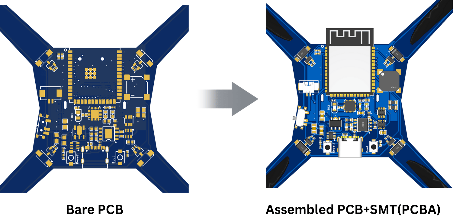
- A PCB is a blank board—etched copper, no components.
- A PCBA is a fully assembled board—ready to test, ready to ship.
The distinction is important—much more than one would suspect. The choice between procuring just the PCB versus an entire PCBA can affect every single element of your workflow—stack-up preference, component source availability, test coverage and cost modeling, along with logistics and yield.
If you skip planning, it's going to get expensive: a board that passes E-test on a bench could fail in the assembly line, fail due to unacceptable land patterns, thermal management, or component source differences. A quality PCBA partner will identify the design issues early on, provide alternatives and recommendations, and stabilize the production process before ramping to production.
PCBA vs PCB: Comprehensive Comparison Table At a Glance
To understand the core differences between PCBA and PCB in a practical context, this table provides a direct comparison of a bare Printed Circuit Board (PCB) and a fully assembled Printed Circuit Board (PCBA) across key technical and logistical parameters.
| Category | PCB (Printed Circuit Board) | PCBA (Printed Circuit Board Assembly) |
|---|---|---|
| Definition | Fabricated laminate board with patterned copper; no components | PCB populated with SMD/THT parts, soldered, inspected, and tested |
| Function | Provides mechanical support and interconnects | Executes designed functionality as an electronic circuit |
| Composition | Core/prepreg (FR‑4, Rogers, etc.), copper, solder mask, silkscreen, surface finish | PCB + components (ICs, passives, connectors), solder joints, flux residues cleaned per spec |
| Manufacturing Flow | Imaging/etch, drilling, plating, lamination, surface finish, profiling, bare‑board test | Solder paste print → SPI → PnP → reflow (or wave/selective) → AOI/X‑ray → ICT/FCT |
| Equipment | LDI, CNC drill/router, PTH plating, AOI for bare board, flying probe test | Stencil printer, SPI, pick‑and‑place, reflow oven, wave/selective solder, AOI, AXI, ICT |
| Design Emphasis | Stack‑up, impedance, clearances, copper balancing, thermal reliefs | BOM health, component availability, land pattern, DFM/DFT, process windows |
| Testing Level | Electrical continuity/isolation (E‑test), visual inspection | AOI/AXI, ICT, flying probe, boundary‑scan, FCT, burn‑in (as needed) |
| Typical Lead Time | 1– 2 days (Achievable with JLCPCB) | 2-3 days (Achievable with JLCPCB) |
| Cost Drivers | Layer count, materials, trace/space, vias, finish (ENIG/OSP/HASL), yield | PCB cost + components + assembly steps + yield loss + testing coverage |
| Packaging/Logistics | Vacuum‑sealed, desiccant, flat stacks | Bubble wrap, palletizing, and anti-static bags. |
| Use Stage | Pre‑assembly validation, mechanical fit, basic continuity | Functional prototypes, EVT/DVT/PVT, production, service spares |
Also Read:
How to Run a Design Rule Check (DRC) for Your PCBs
What is PCB Via and Which Type Should You Choose?
Choose PCBA vs PCB Services
Understanding the technical differences between a PCB and a PCBA is the first step. The next step is applying that knowledge to make the right procurement decision. Ultimately, your selection will be driven by what your project requires in terms of stage of development, complexity, and scale.
When to Order Bare PCBs
Bare PCBs may be the appropriate choice when you plan to procure and assemble your own components. These are often preferred in the following situations:
- Manual Prototyping & R&D: For engineers who are near the beginning of their project development cycle, ordering bare boards affords the greatest amount of flexibility. This option allows for manual debugging, cycling through different strategies for components, and having the capability to change a circuit quickly without the lead time of a whole board assembly.
- Educational, or Hobbyist, Projects: For students or electronics enthusiasts who are learning soldering and building circuits, manually assembling a board is a truly valuable experience. It helps one to further understand how electronic components work together to form device functionality.
- High-security, or proprietary, Assembly: In industries such as aerospace, or medical devices, assembly may need to occur in-house on a certified and secured manufacturing line. In these cases, the overall company will procure bare board from a fabricator and then will conduct the proprietary assembly in-house.
When To Use Turnkey PCB Assembly Services
Turnkey PCB assembly service is a supplier-managed service for a PCB assembly that includes PCB fabrication, component sourcing, and assembly as a single vendor service. This is the typical process for professional product development and is generally recommended in the following situations:
- Large Scale Manufacturing: If the goal is no longer assembling a few prototypes but starting a production run of hundreds or thousands of product units, manual assembly is no longer practical or efficient. Turnkey PCB Assembly services use automated machinery to accomplish these tasks with speed, consistency, and scalability.
- Complex Designs: As electronics become more complex, they often include fine-pitch components, Ball Grid Arrays (BGAs), and 0201 packages, which make placement and soldering almost impossible by hand. Automated Surface Mount Technology (SMT) assembly is often required to achieve the precision necessary to meet the specifications of these complex designs.
- Supply Chain Management: One of the biggest benefits of a turnkey service is the huge reduction in logistical overhead. Instead of having to manage multiple vendors for boards and dozens of component distributors, it is all one point of contact. This represents the most valuable engineering time saved, decreased lead times, and decreases the risk of supply chain disruption.
To simplify the decision, consider the following matrix:
PCBA vs. PCB Services
| Scenario/Requirement | Best Choice: Bare PCB | Best Choice: Turnkey PCBA |
|---|---|---|
| Project Stage | R&D, one-off prototypes, educational projects | Small-batch production, mass production |
| Assembly Complexity | Simple designs with large, easy-to-solder THT components | Designs with fine-pitch SMDs, BGAs, or high component density |
| Supply Chain Preference | You prefer to source and manage all components yourself | You want a single vendor to handle all logistics and assembly |
Choosing a Reliable PCB/PCBA Manufacturer
The dependability and quality of your final electronic product can be guaranteed only through the capabilities of your manufacturing partner. This is a vitally important engineering decision beyond just finding the best price, as a truly dependable manufacturing partner provides a combination of demonstrated technical capabilities, proven quality certifications (ISO, UL, etc.), reliable sourcing for components, and integrated workflows to minimize friction between fabrication and assembly.
Navigating these requirements, though, can be complicated, and this is the reason an integrated one-stop manufacturing partner has become the standard in the industry for efficient product development.
JLCPCB's Integrated PCB Fabrication and Assembly Services
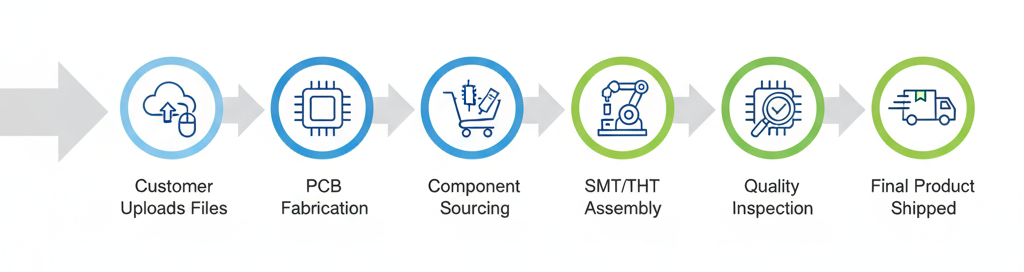
JLCPCB's one-stop turnkey PCB assembly service workflow from file upload to final shipment.
JLCPCB offers a truly one-stop solution, combining high-precision PCB fabrication with professional prototype and PCB assembly services under one roof.
From board manufacturing, global component sourcing, and final assembly to quality inspection, JLCPCB streamlines every stage of your workflow — transforming your PCB design into an assembled circuit board quickly and reliably.
As a leading PCB manufacturer, JLCPCB specializes in producing complex, multi-layer PCBs and high-quality Flexible PCBs for compact designs without sacrificing performance.
In addition to PCB fabrication and assembly, JLCPCB also provides professional PCB layout services, backed by extensive development of the EasyEDA PCB design software to help engineers and product developers bring their ideas to life more efficiently.
See More: Capabilities of JLCPCB PCBA Service
PCB vs. PCBA: The Core Relationship
The easiest way to think about the relationship is like building a house. A PCB is the foundation, frame, and pre-laid wiring paths. It’s essential, but it can’t do anything on its own. A PCBA is the finished house with the power on, plumbing working, and appliances installed—it's fully functional and ready to be used.
Their relationship is both sequential and inclusive:
- Foundation vs. Function: A PCB is the bare, non-functional foundation. A PCBA is a PCB that has been fully populated with components, bringing the circuit design to life.
- Process Flow: The process always flows in one direction: PCB fabrication to PCBA assembly. You simply can't have a PCBA without first manufacturing the bare PCB it's built on.
- Inclusivity: A PCBA includes a PCB. The final cost and complexity of a PCBA are always greater because it is the sum of the PCB + All Sourced Components + Assembly Labor.
FAQs
Q: What's the difference between a PCBA and an Integrated Circuit (IC)?
An Integrated Circuit (IC) is a single electronic component, like one brick in a building. A PCBA (Printed Circuit Board Assembly) is the complete functioning circuit board containing many components, including ICs, resistors, capacitors, connectors, and more. The IC is only one part of the overall PCBA.
Q: How does the choice between SMT and THT affect the final PCBA cost?
The cost difference mainly comes down to automation versus manual labor. SMT (Surface Mount Technology) assembly is highly automated and more cost-effective for mass production. THT (Through-Hole Technology) assembly often requires more manual soldering and labor, increasing production costs, although it can be easier for prototyping and high-strength applications.
Q: What are the three primary files needed for a turnkey PCBA order?
A turnkey PCBA order typically requires three essential manufacturing files:
- Gerber Files – The PCB manufacturing blueprint
- Bill of Materials (BOM) – The complete component list
- Centroid (Pick-and-Place) File – Component placement coordinates used by SMT machines
Q: What are common defects in PCBA and how are they tested for?
Common PCBA defects include solder bridges, open circuits, insufficient solder joints, and incorrect component placement. Manufacturers typically detect these problems using:
- AOI (Automated Optical Inspection) for visual inspection
- ICT (In-Circuit Testing) for electrical testing and fault detection
Conclusion
Understanding the key differences between a PCB and a PCBA empowers anyone involved in electronics to plan projects more effectively, create accurate budgets, and communicate with PCB manufacturers like a professional.
Knowing whether you need a bare printed circuit board or a complete turnkey PCB assembly is essential for a smooth and efficient product development process.
Popular Articles
• How to Identify SMD LED Polarity: Markings, Testing, and PCB Tips
• How to Create a Bluetooth-Controlled Car With Arduino: A Step-by-Step Guide
• How to Design and Assemble a Reliable ESP32 Module PCB on a 2-Layer Board
• The Ultimate Guide to Relay Symbol: Coil, Contacts, Diagrams, and Circuit Applications
• The Ultimate Guide to PCBA: Process,Types and Techniques for the Electronics Enthusiast
Keep Learning
How to Design an ESP32-S3 Development Board from Scratch: A 4-Layer PCB Design Tutorial
Designing your own ESP32-S3 development board gives you complete control over your hardware architecture while preparing your IoT projects for commercial production. Instead of relying on bulkier, off-the-shelf boards, building a custom design allows you to optimize the board space, expose only the required GPIO pins, and integrate peripherals directly onto a single substrate. In this tutorial, we will design a 4-layer ESP32-S3 development board from scratch. We will walk through the entire hardware d......
Circuit Breaker Symbols Explained: IEC, ANSI, MCB, and Pole Configuration Symbols
Electrical schematics are the universal language of power systems, control circuits, and printed circuit boards. Within these diagrams, the circuit breaker symbol is one of the most critical elements. Getting it right is essential for safety, troubleshooting, and manufacturing. An error as simple as mixing up a circuit breaker with a manual switch or an isolator can lead to catastrophic misinterpretations on the factory floor or during field maintenance. This guide provides a complete, technically acc......
How to Identify SMD LED Polarity: Markings, Testing, and PCB Tips
Surface-mount LED components are ubiquitous in electronics design, serving as everything from simple power indicators to complex lighting arrays. Unlike standard resistors, LEDs are polarized diodes. Identifying SMD LED polarity correctly is critical for prototype troubleshooting and high-volume PCB assembly. A reversed LED results in no light output, broken circuit paths, and potential diode breakdown if the reverse voltage exceeds the component's maximum rating (typically 5V or less for most indicat......
Arduino LED Driver Tutorial: Control More LEDs with 74HC595 and MAX7219
Arduino GPIO pins run out quickly in larger LED projects. By utilizing dedicated LED drivers and expansion ICs, you can drastically reduce pin usage, eliminate processor-heavy multiplexing loops, and simplify display wiring. In this guide, you will learn the operational architecture, wiring configurations, cascading techniques, and optimization strategies for the 74HC595 shift register and the MAX7219 LED driver. Why Arduino Projects Need LED Driver ICs Arduino GPIO and Current Limitations An ATmega32......
How to Create a Bluetooth-Controlled Car With Arduino: A Step-by-Step Guide
This tutorial walks through the complete engineering and implementation of a two-wheel Bluetooth RC car with an Arduino Nano module on a specially designed PCBA (Printed Circuit Board Assembly). While many hobbyists start by wiring motors and Bluetooth modules with jumper cables on a breadboard, this approach is prone to disconnection and signal noise. This guide upgrades that process by teaching you how to design a professional mainboard. Key Design Features Controller: Arduino Nano used as a plug-in......
Fiducial Marks in PCB and SMT Assembly: A Complete Guide to Accuracy and Design Rules
Modern Printed Circuit Boards (PCBs) are complex, integrating high-density components like 0.4mm pitch Ball Grid Arrays (BGAs), 0201 passives, and fine-pitch Quad Flat No-Lead (QFN) packages. In this advanced manufacturing environment, achieving placement accuracy measured in micrometers is crucial. A significant challenge in automated manufacturing is how pick-and-place machines, which handle thousands of components per hour, precisely locate the PCB. A board on a conveyor system is never in the perf......