How to Design an ESP32-S3 Development Board from Scratch: A 4-Layer PCB Design Tutorial
13 min
- Custom ESP32-S3 Development Board Hardware Specifications
- Step 1: Design the ESP32-S3 Development Board Schematic
- Step 2: Plan a 4-Layer PCB Stack-Up for ESP32-S3 Development Board
- Step 3: Place Components on the PCB
- Step 4: Route the ESP32-S3 PCB
- Step 5: Add Ground Copper Pours and Via Stitching
- Step 6: Run Final PCB Checks and Design Rule Check (DRC)
- Step 7: Generate ESP32-S3 PCB Manufacturing Files
- Step 8: Order Your ESP32-S3 Development Board from JLCPCB
- Step 9: Assemble the ESP32-S3 Development Board
- ESP32-S3 Development Board PCB Manufacturing Workflow
- Conclusion
- FAQs about ESP32-S3 PCB Design

Designing your own ESP32-S3 development board gives you complete control over your hardware architecture while preparing your IoT projects for commercial production. Instead of relying on bulkier, off-the-shelf boards, building a custom design allows you to optimize the board space, expose only the required GPIO pins, and integrate peripherals directly onto a single substrate.
In this tutorial, we will design a 4-layer ESP32-S3 development board from scratch.
We will walk through the entire hardware development pipeline: structuring the ESP32-S3 schematic, planning a robust 4-layer stack-up, applying routing best practices, and preparing manufacturing-ready files for fabrication and assembly through JLCPCB.
The completed board features:
- ESP32-S3-WROOM module (Wi-Fi and Bluetooth LE 5.0)
- CP2102 USB-to-UART interface for standard programming and debugging
- Native USB OTG Type-C connector for high-speed USB applications
- Automatic boot/download circuit (no manual button pressing required)
- AMS1117-3.3 V regulator with proper thermal and noise filtering
- Tactile Reset and Boot buttons for manual hardware control
- Onboard status LEDs (Power indicator and a user-programmable GPIO2 LED)
- TVS diode arrays for robust ESD protection on both USB interfaces
- Dual 20-pin headers rail spaced for breadboard compatibility
- 4-layer PCB architecture featuring dedicated internal ground and power planes
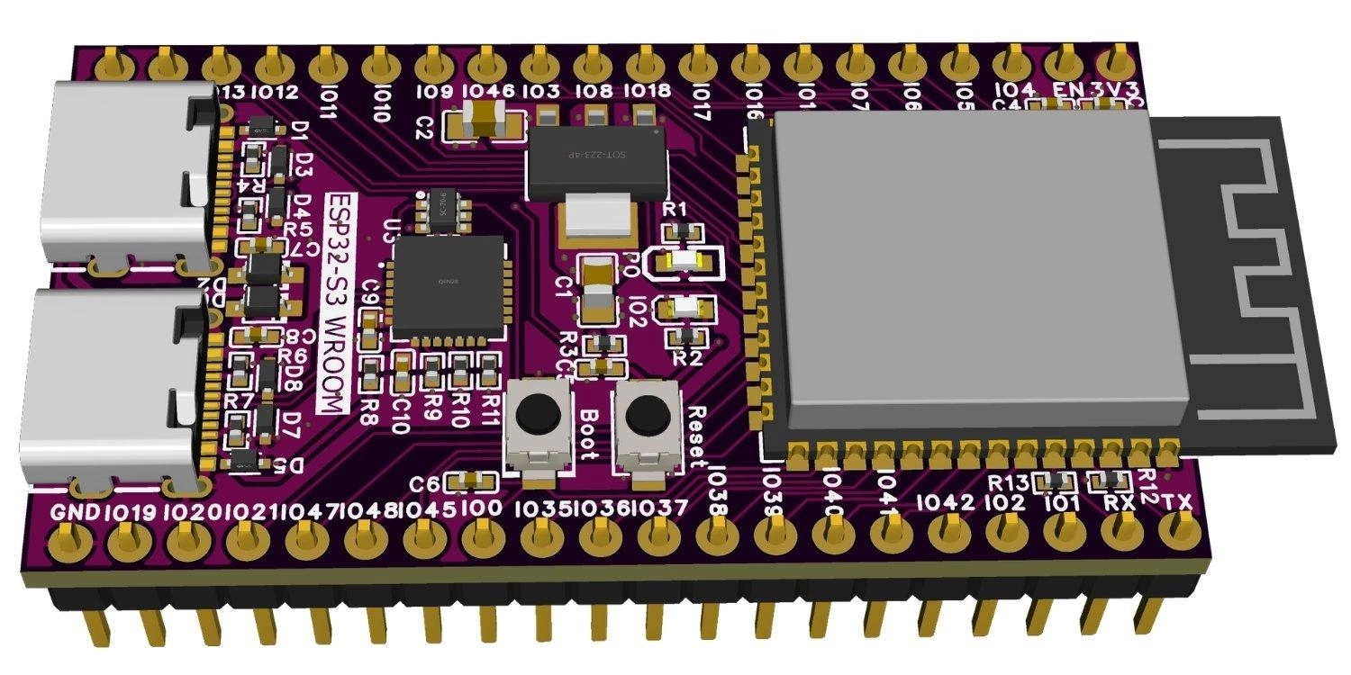
Figure: Finished 4-layer ESP32-S3 development board with dual USB Type-C connectors.
Custom ESP32-S3 Development Board Hardware Specifications
| Feature | Specification |
|---|---|
| MCU | ESP32-S3-WROOM |
| PCB Layers | 4 Layers (Signal - GND - PWR - Signal) |
| Programming Interface | CP2102 USB-to-UART Bridge |
| Native USB Support | USB Type-C OTG Interface |
| Power Input | USB Type-C (5 V nominal) |
| Voltage Regulator | AMS1117-3.3 V Low Dropout (LDO) |
| GPIO Headers | 2 x 20 Pins (2.54 mm pitch) |
| Form Factor | Breadboard Compatible |
Step 1: Design the ESP32-S3 Development Board Schematic
Before diving into the PCB layout, we must establish a robust schematic. Breaking the schematic down into modular, functional blocks simplifies design verification and future troubleshooting.
If you have previously explored how to design an ESP32-S2 module PCB, you will find the core ESP32-S3 setup highly intuitive, though the S3 architecture introduces distinct pin allocations and dual-core capabilities that make precise schematic planning crucial.
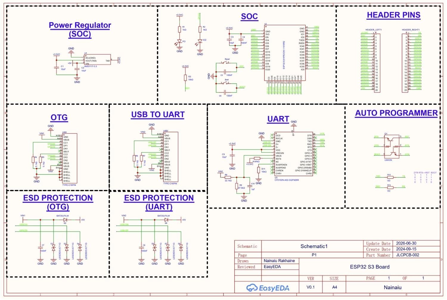
Figure: Complete schematic of the ESP32-S3 development board.
ESP32-S3 Core Circuit
The heart of our board is the ESP32-S3-WROOM module. Following Espressif’s hardware design guidelines, we configure the core module with:
- An RC delay circuit on the EN (CHIP_PU) pin to ensure a stable startup delay.
- Necessary pull-up resistors on GPIO0 to keep the boot mode configuration predictable.
- Tactile tactile buttons for manual hardware reset and boot selection.
ESP32 Power Supply
The board is powered via the 5V VBUS line of our USB-C ports. An AMS1117-3.3 linear regulator steps down this 5 V input to a clean 3.3 V system rail.
To prevent voltage drops during high-power Wi-Fi TX bursts, we place a 10 uF bulk electrolytic or tantalum capacitor on the regulator's input, paired with a 10 uF ceramic capacitor at the 3.3 V output. A dedicated red LED is connected in series with a current-limiting resistor directly to the 3.3 V rail as a visual power indicator.
USB Programming Interface
For effortless firmware deployment and serial monitoring, we include a dedicated USB-to-UART bridge using the CP2102 IC. The CP2102 handles USB-to-serial conversion, bridging the RX/TX pins of the ESP32-S3's UART0.
To easily source passives, transistors, and ICs like the CP2102 for this portion of your design, you can browse verified inventories directly in the JLCPCB Parts Library.
Automatic Programmer Circuit
To eliminate the inconvenience of manually pressing buttons, an automatic programmer circuit is integrated. Using two generic NPN transistors driven by the DTR and RTS signals, the circuit pulls EN and GPIO0 low to enter bootloader mode.
Native USB OTG
The ESP32-S3 features an internal, full-speed USB OTG peripheral. We route these native lines directly to a secondary USB Type-C connector, using 5.1 kOhm pull-down resistors on CC pins.
USB Protection
Since USB ports are targets for static discharge, we place low-capacitance ESD protection diode arrays immediately behind the VBUS, D+, and D- pins to shunt transient voltage spikes to ground.
GPIO Headers
To expose the ESP32-S3’s functional pins, we route them to two 20-pin male headers. The pin rows are spaced exactly 0.9 inches (22.86 mm) apart, leaving one row of breadboard holes exposed on each side of the board when inserted.
Status LEDs
Two onboard LEDs are included to assist in visual debugging:
| LED | Function | Configuration |
|---|---|---|
| Power LED | 3.3 V Supply Indicator | Connected to the 3.3 V rail via a 1 kOhm resistor. |
| GPIO2 LED | User-Programmable LED | Active-high LED tied to GPIO2 for quick "Blink" tests. |
Table: Onboard status LEDs used in the ESP32-S3 development board.
Decoupling Capacitors
To maintain stable power delivery, decoupling capacitors must be placed across the power inputs of every IC on the board:
| Capacitor | Purpose | Placement |
|---|---|---|
| 100 nF | Local High-Frequency Decoupling | Placed immediately next to every VCC/3.3V pin. |
| 1 uF | Intermediate Frequency Filtering | Placed adjacent to the main ESP32-S3 VDD pin. |
| 10 uF | Bulk Energy Storage | Placed near the output of the LDO and main power inputs. |
| AMS1117 Capacitors | Regulator Stability | Placed as close as possible to the input/output pins of the regulator. |
Table: Decoupling capacitors used throughout the ESP32-S3 development board.
Step 2: Plan a 4-Layer PCB Stack-Up for ESP32-S3 Development Board
With the schematic finalized, the design transitions to the ESP32-S3 PCB layout phase.
For high-speed wireless microcontrollers like the ESP32-S3, a 4-layer PCB stack-up is highly recommended over a traditional 2-layer design. The internal planes provide continuous return paths for high-frequency signals, reducing Electromagnetic Interference (EMI) and maintaining impedance control for the USB data lines.
The stack-up configuration for this board is as follows:
| Layer | Type | Function |
|---|---|---|
| Top Layer | Signal | Component footprints, RF antenna clearance, and primary signal routing. |
| Layer 2 | Plane | Solid, uninterrupted Ground (GND) plane for shielding and short return paths. |
| Layer 3 | Plane | Dedicated 3.3 V Power Plane to simplify power distribution. |
| Bottom Layer | Signal | Secondary routing, return-path stitching, and auxiliary test points. |
Table: Four-layer PCB stack-up for the ESP32-S3 development board.
Step 3: Place Components on the PCB
Strategic component placement is the foundation of a clean, noise-free board design. All active and passive components on this board are placed on the Top Layer to streamline manufacturing and significantly lower assembly costs.
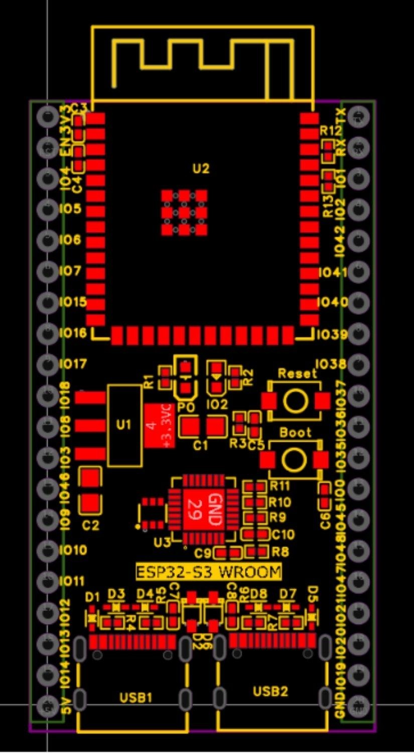
Figure: Component placement of the ESP32-S3 development board before routing.
Key Component Placement Rules:
- The ESP32-S3 Module: Position the module at one end of the PCB. The PCB copper planes and tracks must not extend underneath the module's onboard PCB antenna. Leave this "keep-out" zone completely free of copper across all four layers to avoid degrading wireless signal range.
- USB-C Connectors: Align both USB Type-C connectors flush with the board edge. Place the CP2102 closely behind the programming USB port to keep the USB differential signals as short and direct as possible.
- Power Circuitry: Keep the AMS1117 regulator and its decoupling capacitors in close proximity to the USB 5 V input. This keeps high-current loops localized to a small area of the board.
- Decoupling Capacitors: Place every 100 nF bypass capacitor directly next to its target power pin. The trace must run from the power source, through the capacitor pad, and then into the IC pin, with a ground via located immediately next to the capacitor's ground pad.
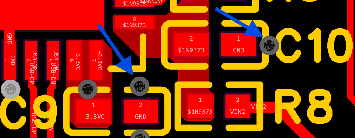
Figure: Place the decoupling capacitor close to the target IC, with a ground via next to the capacitor's ground pad for the shortest return current path.
Step 4: Route the ESP32-S3 PCB
Routing translates your schematic connections into physical copper traces. We must pay special attention to differential pairs and power routing.
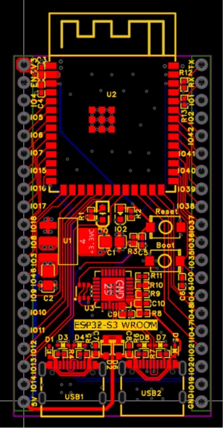
Figure: Routed ESP32-S3 PCB showing signal traces and power routing.
1. Route Critical Signals First
Route the USB differential pairs before the remaining signals. Use the JLCPCB PCB Impedance Calculator to determine the required trace width and spacing for your PCB stack-up. In this design, a 6 mil trace width and 10 mil gap achieve the target 90 Ω differential impedance. Keep the D+ and D− traces parallel with matched lengths, and avoid vias whenever possible.
.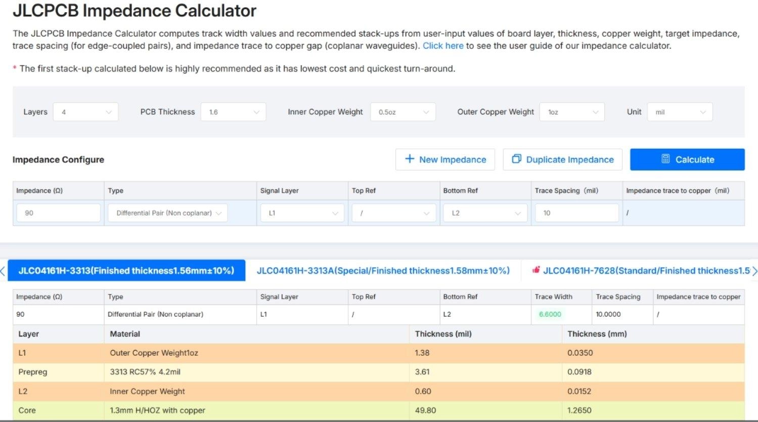
Figure: JLCPCB PCB Impedance Calculator configured for a 90 Ω USB differential pair with 6 mil traces and a 10 mil gap.
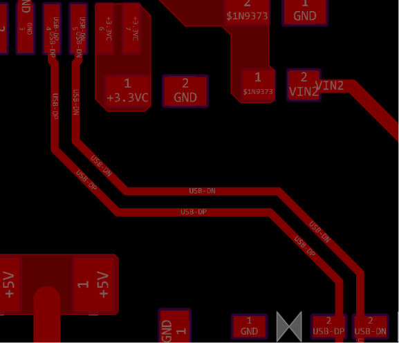
Figure: 90 ohm impedance Differential Pair Routing for USB
Try to maintain equal length for differential routing. If not equal, you have to manually perform equal length tuning through the software.
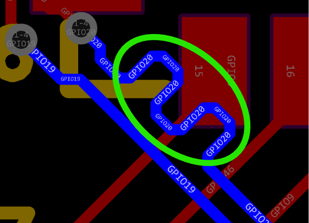
Figure: Equal length tuning to match the differential pair traces length
2. Connect to the Power and Ground Planes
Instead of routing thin 3.3 V traces across the entire board, we use vias to drop directly down to the Layer 3 power plane. For the ground connections, drop vias directly to the Layer 2 ground plane. This low-impedance connection dramatically decreases parasitics.
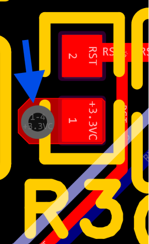
Figure: 3.3v Via with traces connecting with power plane
3. Size PCB Traces for Current Carrying Capacity
Ensure signal traces are kept at a standard width (typically 6 to 8 mils). Power lines must be routed with thicker traces (at least 15 to 25 mils) or handled entirely via dedicated polygon pours to safely carry up to 500 mA during wireless transmission.
Step 5: Add Ground Copper Pours and Via Stitching
Once routing is complete, we add solid ground copper pours to the Top and Bottom signal layers.
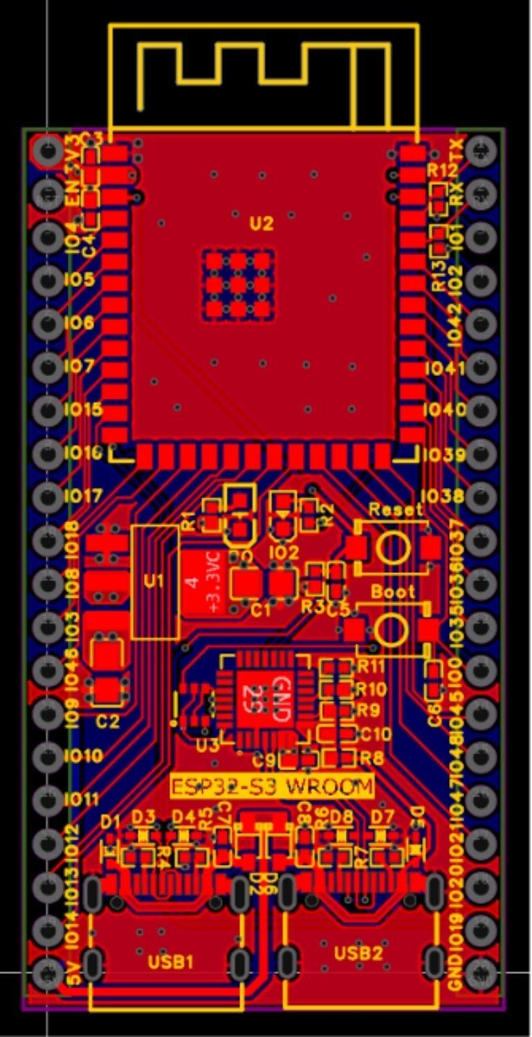
Figure: Completed ESP32-S3 PCB with ground pours and stitching vias.
These copper pours act as shielding. To tie all ground regions together, perform via stitching. Add ground vias around the board perimeter every 2 to 3 mm to create a Faraday cage effect that minimizes EMI.
Step 6: Run Final PCB Checks and Design Rule Check (DRC)
Before outputting any fabrication files, complete the following visual and automated checks:
- Silkscreen Cleanup: Label all GPIO pins with clear, legible text on the top silkscreen. Mark the Reset (RST) and Boot (BOOT) buttons, and add polarity markings for status LEDs.
- Design Rule Check (DRC): Run your PCB design software's DRC using the exact clearance, minimum trace width, and drill hole constraints provided by your manufacturer. This guarantees the board falls within standard fabrication tolerances.
Step 7: Generate ESP32-S3 PCB Manufacturing Files
After the layout passes DRC, you need to export the files required for production.
For standard PCB fabrication, generate:
- Gerber Files
- Excellon Drill Files
If you plan to utilize an automated assembly service to save hours of manual soldering, you will also need to export:
- Bill of Materials (BOM): A spreadsheet detailing part numbers, designators, and packages.
- CPL / Centroid File: A file containing the exact X-Y coordinates and rotation angles of every component on the board.
Before finalizing your exports, double-check that your component footprints match the specific part packages in your BOM.
Step 8: Order Your ESP32-S3 Development Board from JLCPCB
With files in hand, the ordering process is simple:
- Go to the JLCPCB Quote Page and upload your compiled Gerber zip file.
- The online Gerber viewer will parse your files and display a real-time visual preview of your board layers, drill holes, and dimensions.
- Configure your physical manufacturing specifications:
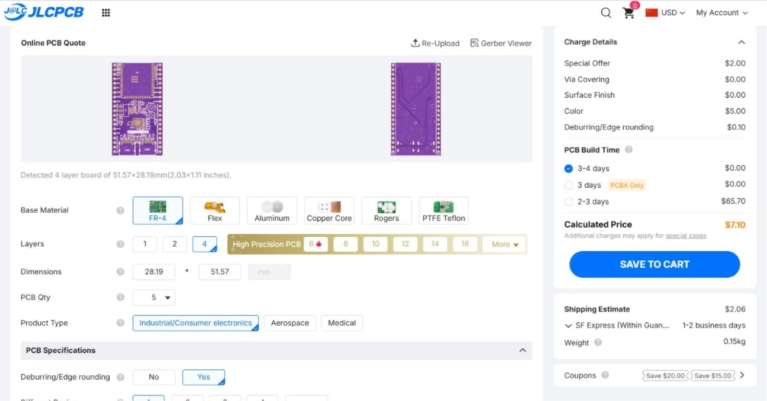
Figure: Uploading Gerber files to JLCPCB for PCB fabrication.
For most prototyping runs, standard settings work best:
- PCB Thickness: 1.6 mm (or 1.2 mm for a slightly thinner profile)
- Solder Mask Color: Green, Blue, Black, Red, or Yellow (does not affect price)
- Surface Finish: HASL (with lead) for basic prototypes, or ENIG (Electroless Nickel Immersion Gold) for flat pads and superior solderability.
Step 9: Assemble the ESP32-S3 Development Board
Rather than hand-soldering fine-pitch components like the CP2102 and the USB-C connectors, opting for JLCPCB PCB Assembly is highly recommended.
Rather than hand-soldering fine-pitch components, opting for JLCPCB PCB Assembly is highly recommended. Upload your generated BOM and Pick and Place (CPL) files.
During assembly, the factory runs a highly automated SMT line where solder paste is applied through a precision steel stencil, parts are accurately positioned using pick-and-place machines, and the board is processed in a multi-zone reflow soldering oven to form perfect electrical connections.
ESP32-S3 Development Board PCB Manufacturing Workflow
| Step | Action | Key Deliverable / Outcome |
|---|---|---|
| 1 | Schematic Design | Define circuitry, ESP32 connections, and ESD protection. |
| 2 | PCB Layout & Routing | Place parts, route 90 Ohm USB differential pairs, run DRC. |
| 3 | Manufacturing Export | Generate Gerber, NC Drill, BOM, and Pick & Place (CPL) files. |
| 4 | Quote & Upload | Upload Gerbers to the JLCPCB Quote Page. |
| 5 | Parameter Selection | Select layer count, board thickness, and solder mask color. |
| 6 | PCBA Setup (Optional) | Upload BOM/CPL files to set up automated SMT assembly. |
| 7 | Production & Quality | Stencil printing, automated placement, reflow soldering, and AOI inspection. |
| 8 | Delivery | High-quality, fully assembled development boards delivered to your door. |
Table: Complete workflow from PCB design to manufacturing through JLCPCB.
Conclusion
Designing your own custom ESP32-S3 development board is a highly rewarding milestone in your hardware engineering journey. Transitioning from a simple 2-layer layout to a robust 4-layer architecture ensures your wireless application has clean power rails, excellent thermal performance, and superb wireless range.
By following this systematic design workflow - from careful schematic blocks to optimized component placement, proper trace sizing, differential routing, and design rule verification - you reduce the risk of board spins and hardware bugs. With the convenience of automated assembly services, taking your prototypes from the screen to a fully assembled board in your hands is faster and more reliable than ever before.
FAQs about ESP32-S3 PCB Design
Q: Why is a 4-layer PCB design preferred over a 2-layer design for the ESP32-S3?
The ESP32-S3 is a high-frequency system-on-chip with on-board Wi-Fi and Bluetooth. A 4-layer PCB provides dedicated ground and power planes directly underneath the signal layers, which drastically reduces electromagnetic interference (EMI), minimizes loop inductance, and helps control trace impedance.
Q: Do I need to route the USB-C data traces with precise impedance?
Yes. The ESP32-S3 native USB and CP2102 USB lines operate as high-speed differential pairs. To prevent signal reflections and data corruption, these lines should be routed as a differential pair with a target differential impedance of 90 Ohms.
Q: Why is there an antenna keep-out area under the ESP32-S3 module?
The ESP32-S3-WROOM module uses an onboard inverted-F PCB antenna. Any copper planes, tracks, or components underneath or near this antenna area will shield or detune the RF signals, severely reducing your Wi-Fi and Bluetooth wireless range.
Q: How do I verify that my custom PCB footprints are correct before ordering?
You should always cross-check the physical footprints against the manufacturer's datasheet. Additionally, exporting your design as a 3D model (STEP file) or using your CAD software's 3D viewer is an excellent way to visually confirm component sizes and alignment before submitting your files for manufacturing.
Popular Articles
• Logic Gate Symbols: The Complete Chart, Truth Tables [2026]
• How to Design and Assemble a Reliable ESP32 Module PCB on a 2-Layer Board
• How to Identify SMD LED Polarity: Markings, Testing, and PCB Tips
• The Ultimate Guide to Relay Symbol: Coil, Contacts, Diagrams, and Circuit Applications
• Power Supply Symbols Chart: A Complete Guide to AC, DC, Ground, Battery, and Source Symbols
Keep Learning
How to Read Resistor Color Code: Complete Guide with Chart and Examples
4-Band Resistor Color Code Explained A 4-band resistor color code is one of the most common methods used to indicate resistance values in electronic components. It is widely used to help engineers and hobbyists quickly determine resistance values without using a resistor color code calculator. In a standard 4-band resistor: First Band (Digit 1): Represents the first significant digit Second Band (Digit 2): Represents the second significant digit Third Band (Multiplier): Indicates the factor by which t......
Solder Paste vs Flux: What's the Difference and When Should You Use Each?
Solder paste and flux are not interchangeable. Solder paste contains solder alloy powder and flux, while flux contains no solder alloy. This difference matters when choosing materials for SMT, reflow soldering, or manual soldering. Flux removes metal oxides and prevents re-oxidation, allowing molten solder to wet copper pads and component leads properly. Solder paste combines flux with fine solder alloy powder. During reflow, the flux activates to improve wetting while the solder alloy melts to form t......
Fiducial Marks in PCB and SMT Assembly: A Complete Guide to Accuracy and Design Rules
Modern Printed Circuit Boards (PCBs) are complex, integrating high-density components like 0.4mm pitch Ball Grid Arrays (BGAs), 0201 passives, and fine-pitch Quad Flat No-Lead (QFN) packages. In this advanced manufacturing environment, achieving placement accuracy measured in micrometers is crucial. A significant challenge in automated manufacturing is how pick-and-place machines, which handle thousands of components per hour, precisely locate the PCB. A board on a conveyor system is never in the perf......
Ground Symbols Explained: Earth, Chassis, Signal, Analog, Digital Ground & More
Key Takeaways ⬇ Download the Ground Symbol Cheat Sheet (PDF) Keep all six ground symbols and their standard numbers on one page for quick reference. Four IEC 60417 symbols: IEC 60417 defines symbol 5017 for earth, 5018 for functional earth, 5019 for protective earth, and 5020 for frame/chassis. Protective earth is safety-related: IEC 60417-5019 identifies the protective earth connection and is used for safety-related protective bonding. Signal ground uses a different convention: IEEE Std 315 defines t......
How to Choose an ESP32 Development Board: A Beginner-Friendly Guide
The leap from blinking a simple LED to building a cloud-connected smart home device is a thrilling milestone for any electronics beginner. At the heart of this transition is often one undisputed champion: the ESP32. However, when you first search for an ESP32 development board, you are instantly met with a dizzying array of models, shapes, and specifications. How do you know which one is right for your first IoT (Internet of Things) project? In this beginner's guide, we will break down what makes thes......
How to Design an ESP32-S3 Development Board from Scratch: A 4-Layer PCB Design Tutorial
Designing your own ESP32-S3 development board gives you complete control over your hardware architecture while preparing your IoT projects for commercial production. Instead of relying on bulkier, off-the-shelf boards, building a custom design allows you to optimize the board space, expose only the required GPIO pins, and integrate peripherals directly onto a single substrate. In this tutorial, we will design a 4-layer ESP32-S3 development board from scratch. We will walk through the entire hardware d......