Mastering PCB Plating Types and Process Control in High-Yield Fabrication
17 min
- Fundamental Principles of Plating on PCBs
- Major PCB Plating Types and Fabrication Techniques
- Step-by-Step Breakdown of the PCB Plating Process
- Preventing Critical Plating Defect Risks
- JLCPCB's Precision Plating Infrastructure & Quality Assurance
- FAQs about PCB Plating
- Conclusion
Key Takeaways
- Two-Step Plating: Chemical seed layer comes first, electrolytic copper adds structural strength.
- Process Choice: Pattern plating enables fine tracks; panel plating suits heavy copper.
- Via Integrity: Keep aspect ratio ≤ 10:1 to prevent thinnest-point barrel cracking.
- Surface Finishes: Use ENIG for flat BGA pads and hard gold for high-wear contacts.
- IPC Standards: Class 2 mandates 20μm copper wall thickness; Class 3 requires 25μm with zero voids.
PCB plating turns a stack of drilled laminate into a working circuit. It is also the one step you can never inspect from the outside. Every via on your board is a hole with a copper tube grown inside it. Once the solder mask goes down, you will never see that tube again. Here is the intuition that makes the rest of the subject click into place. Copper does not stick to cured epoxy, and epoxy does not conduct, so the fab has to grow a chemical seed layer on the bare resin first.
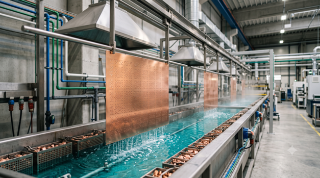
Figure 1: Panels moving through a vertical continuous copper plating line
Only then can electric current be carried through the thickness that actually matters. That two-stage trick, chemistry first and current second, explains almost every plating type, defect, and inspection rule you will meet. This guide covers how those two mechanisms differ and what separates pattern plating from panel plating. It also covers how finishes such as ENIG and hard gold are deposited. Bath chemistry and current density come last, because they decide whether a deep via survives reflow.
Fundamental Principles of Plating on PCBs
Plating does two jobs that look like one from the outside. It forms vertical connections through drilled holes and protects the exposed copper. Because those two jobs face very different surfaces, the two halves of the process use completely different chemistry.
Chemical Deposition vs. Electroplating Mechanism
A fresh hole that is drilled is an insulating tube. The drill has sliced through the copper layers, but the wall that it has left behind is epoxy resin and glass fiber, and neither is conductive. It cannot be electroplated as it does not conduct electricity yet.
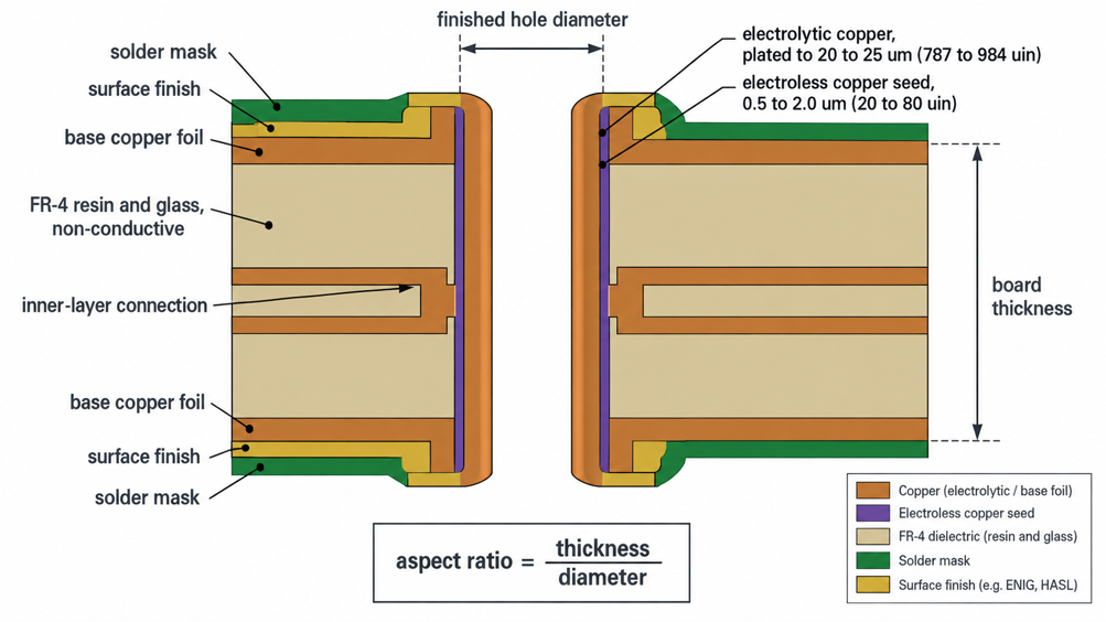
Figure 2: Cross-section of a plated through hole showing every deposited layer
- Electroless copper addresses this issue on a chemical level: In the bath, the copper ions are reduced by the action of the formaldehyde onto any surface carrying the palladium catalyst, without the use of an outside current. The bath has no regard for the surface conduct and will coat resin, glass, and exposed inner-layer copper equally.
- The real thickness is added by electrolytic plating: The panel is immersed in an acidic copper sulfate solution, where it is the cathode and copper is deposited on all surfaces to which it is connected, including the walls of the holes that were freshly seeded. The rate of deposit is about 25 µm/hr per cell; the barrel would be plated to the final wall after about 1 hr of plating. This is the point where you get holes that are truly plated.
Impact of Plating Quality on Current Capacity and Signal Integrity
Current is carried by a wire through a copper barrel, and the thickness of the barrel wall determines the amount of current it can carry. For a 0.3 mm hole, a 25 µm wall gives about 0.024 mm² of copper. This is the equivalent of a 0.67 mm trace in 1 oz copper. Further reduce that wall to 18 µm, and you lose 28% of that cross-section, making the via the smallest point in the path. The mechanical risk is greater than the resistive risk. Below Tg, FR-4 will grow by its thickness at the rate of about 50 ppm/°C; by contrast, copper grows at a rate of 17 ppm/°C.
A wall with a thin patch will focus the strain on that thin patch, and the crack will start at the weakest point in the plating. This is not indicated in a continuity test since the cracked barrel is still touching itself at room temperature. Plating is another factor that is critical to signal integrity. For copper, at 1 GHz, the skin depth is approximately 2.1 µm.
Major PCB Plating Types and Fabrication Techniques
The PCB plating types you will meet are split into three families that do not compete with each other, because each depends on what the one before it left behind.
Overview of Electroless Copper and Electrolytic Plating
Copper Plating Processes
- Electroless copper: An autocatalytic process that deposits a thin conductive copper layer inside drilled holes without external current. It is mainly used to prepare the whole wall for later plating.
- Direct metallization: Uses conductive carbon, graphite, or polymer instead of electroless copper. The conductive film makes the hole ready for electroplating and avoids formaldehyde-based chemistry.
- Electrolytic copper: Uses an electrical current to build the required copper thickness on the surface and inside the hole barrel.
Electrolytic Bath Additives
- Suppressor: Slows deposition on high-current outer surfaces.
- Brightener: Promotes faster deposition in lower-current areas, including the hole center.
- Leveler: Controls excessive buildup at corners and high spots.
Together, these additives improve plating distribution and help produce a more uniform copper thickness through the hole.
Comparative Analysis: Pattern Plating vs. Panel Plating
The difference between pattern plating and panel plating is simply when the panel gets imaged.
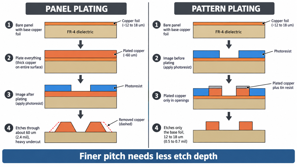
Figure 3: Pattern plating and panel plating process flows side by side
- Panel plating first electroplates the entire copper surface, then applies photoresist and etches the circuits into the thicker copper.
- Pattern plating images first, plates copper only where the resist is open, and covers it with a tin resist before etching.
Etching is what makes them behave differently. Panel plating asks the etchant to remove roughly 60 µm of copper between traces. Pattern plating etches only the thin base foil because the tin resist protects the plated circuitry. Undercut scales with how long the etchant works, so the deeper etch costs you the sidewall. That is why panel plating struggles with lines and spaces below about 0.1 mm (4 mil).
| Aspect | Panel Plating | Pattern Plating | What This Means for Your Design |
|---|---|---|---|
| Imaging order | Plate the whole panel, then image and etch | Image first, then plate only the open areas | Pattern plating needs an extra resist strip step, so the line is longer |
| Copper etched between traces | Base foil plus the full plated thickness, near 60 µm (2.4 mil) | Base foil only, often 12 to 18 µm (0.5 to 0.7 mil) | Less etch depth means less undercut and straighter trace walls |
| Practical line and space | Comfortable down to about 0.1 mm (4 mil) | Reaches 0.075 mm (3 mil) and below | Fine-pitch BGA fanout effectively requires pattern plating |
| Copper thickness uniformity | Very even across the surface | Varies with local pattern density | Panel plating suits heavy copper where flatness matters more than pitch |
| Typical use | Heavy copper, coarse geometry, simple two-layer work | HDI, fine-pitch, most multilayer production | Match the process to your tightest feature, not to your average one |
Surface Finish Plating Options (ENIG, Immersion Silver, Hard Gold)
A surface finish is the last plating step, applied only where the solder mask leaves copper exposed. Bare copper oxidizes within days, and an oxidized pad will not wet with solder. The finish, therefore, exists to keep pads solderable until the board reaches assembly.
ENIG stands for electroless nickel immersion gold, and neither layer is electroplated. The nickel forms a chemical barrier over the copper. The gold is then deposited by displacement, with gold ions swapping places with nickel atoms. That reaction stops once the nickel is covered, which is why ENIG gold is measured in tens of nanometres.
Immersion silver works by the same displacement mechanism but deposits straight onto copper with no nickel barrier. That keeps it flat and cheap, though it stays sensitive to sulfur and to handling.
Hard gold is the odd one out because it is genuinely electroplated and cobalt-hardened for wear. It is thick enough to survive the thousand insertion cycles a DDR4 DIMM or a PCIe card edge connector sees.
See all the finishes available from the table and their properties:
| Finish | Deposited Thickness | Governing Standard | Where It Earns Its Place |
|---|---|---|---|
| ENIG | Nickel 3 to 6 µm (118 to 236 µin), gold 0.05 to 0.1 µm (2 to 4 µin) | IPC-4552 | Fine-pitch BGA and QFN, flat pads, long shelf life |
| Immersion silver | 0.1 to 0.3 µm (4 to 12 µin) | IPC-4553 | Flat, low-loss RF pads at a lower cost than ENIG |
| Hard gold | 0.76 µm (30 µin) and up over nickel | ASTM B488 | Edge connectors and contacts that get plugged repeatedly |
| Immersion tin | 0.8 to 1.2 µm (31 to 47 µin) | IPC-4554 | Press-fit connectors and flat pads, short shelf life |
| OSP | 0.2 to 0.5 µm (8 to 20 µin) | IPC-4555 | Lowest cost, single reflow, high-volume consumer boards |
| HASL, lead-free | Uneven, roughly 1 to 40 µm (0.04 to 1.6 mil) | J-STD-003 | Through-hole and coarse SMD are the cheapest, not for fine pitch |
Gold plated to a full micron costs many times what gold deposited to tens of nanometres does. That is why hard gold is normally restricted to the contact area alone. Our guide to choosing the right surface finish walks through the same trade-off from the assembly side.
Step-by-Step Breakdown of the PCB Plating Process
Almost every plating defect is created before any copper is deposited. The preparation steps decide whether the seed layer adheres evenly, so the electrolytic stage can only build on whatever they leave behind.
Surface Preparation: Cleaning, Micro-Etching, and Activation
Drilling leaves a mess inside the hole, and friction melts resin and smears it across the exposed inner-layer copper. An inner layer can therefore end up insulated by a thin film of its own laminate. Removing that smear is a chemical job rather than a mechanical one, and it comes first.
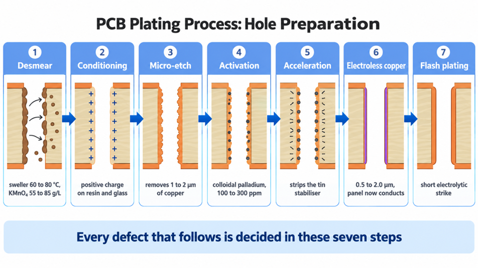
Figure 4: The seven preparation stages of the PCB plating process
The full PCB plating process runs through seven preparation stages before the panel ever sees a plating cell:
- Desmear: A solvent sweller at 60 to 80 °C softens the drill smear. Potassium permanganate at 55 to 85 g/L then oxidizes it away, and a reducer strips the manganese residue.
- Conditioning: A cationic conditioner puts a positive charge on the resin and glass, so the negatively charged catalyst colloid will attach to them.
- Micro-etch: A controlled persulfate or peroxide etch removes 1 to 2 µm of copper, leaving a fresh, slightly roughened surface for adhesion.
- Pre-dip and activation: The panel enters a colloidal palladium bath, typically 100 to 300 ppm, which seeds catalyst particles across every hole wall.
- Acceleration: A mild acid strips the tin stabilizer off the palladium colloid, so the catalyst underneath is exposed and active.
- Electroless copper: The catalyzed surfaces grow 0.5 to 2.0 µm of chemical copper, which makes the panel conductive from one side to the other.
- Flash plating: A short electrolytic strike thickens the fragile seed before the panel queues for the main plating cell.
Conditioning is the stage that quietly decides adhesion, and it is invisible in every inspection you can run afterward. It leaves no measurable layer, so nothing tells you it went wrong until the panel is plated.
Preventing Critical Plating Defect Risks
Plating defects are rarely random. Nearly all of them trace back to something that stopped the solution from reaching a surface, or stopped current from reaching it evenly.
Mitigating Hole Wall Voids and Pitting
A hole wall void is a gap in the copper barrel where no plating has formed at all. It is not a thin spot but a bare dielectric, so whatever current the via carries has to squeeze around it. Pitting is different: a pit is a small crater in copper that usually forms when something lands on the surface of the midplate.
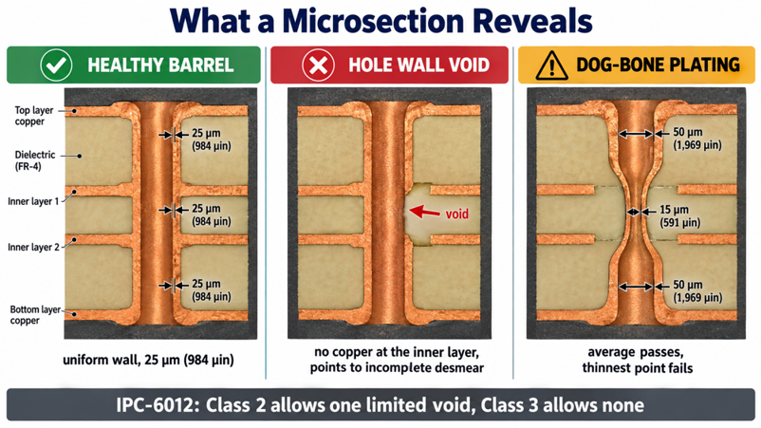
Figure 5: Microsection views of a healthy barrel, a hole wall void, and dog-bone plating
Five causes account for most voids you will ever see on a microsection:
- Trapped air in the hole: A small, deep hole holds a bubble that the solution cannot displace, so nothing plates behind it. Wetting agents and vacuum-assisted or ultrasonic flow break the bubble before the catalyst step.
- Incomplete desmear: Resin left sitting on an inner-layer pad blocks both catalyst and copper, producing a void at exactly the layer you needed to connect.
- Glass fiber protrusion: A fiber bundle standing proud of the wall shadows the surface behind it and resists activation, so the plating simply skips around it.
- Starved or contaminated catalyst: Low palladium concentration leaves patches with no seed, and electroless copper does not start where there is nothing to catalyze it.
- Bath particulates: Suspended solids or organic breakdown products settle on the surface during electroplating and mask a point, leaving a crater in the deposit.
The two signatures point in opposite directions, which makes a microsection worth reading carefully. A void lined up with an inner-layer pad points at desmear or activation, while scattered pits across the whole panel point at bath filtration instead.
Controlling Plating Distribution on High Aspect Ratio Vias
Aspect ratio is board thickness divided by finished hole diameter, and it is the single number that predicts plating trouble. A 1.6 mm board with a 0.2 mm via runs at 8:1. Solution must then travel eight hole diameters to reach the middle from either end. Throwing power measures how well a bat copes with that geometry.
Above roughly 8:1, that figure falls away quickly, and the barrel takes on a dog-bone profile, thick at both entrances and pinched in the center. The average wall thickness can still be measured fine while the thinnest point sits well under specification, which is precisely the condition that leads to cracks in reflow. Aspect ratio is a design variable, not a fab problem, so the fix belongs in your stackup. Keeping a 1.6 mm board's vias at 0.3 mm maintains the ratio near 5:1. JLCPCB's published rule is not to exceed 10:1 for plated through-holes. Our guide to the via aspect ratio sets out where each band starts to bite.
JLCPCB's Precision Plating Infrastructure & Quality Assurance
Plating quality is invisible on a finished board, so what matters is whether the fab measures it and hands you the numbers.
Automated Plating Lines for Consistent Copper Thickness
Vertical continuous plating, usually shortened to VCP, is what makes copper thickness repeatable at volume. Panels hang from a moving conveyor and travel through each cell at a fixed speed while electrolyte is pumped hard across the entire area. Because every panel follows the same path for the same time, panel-to-panel variation becomes a machine setting rather than an operator judgment.
Outer copper weight and hole plating are built in the same cell, so they move together. Choosing a 2-oz outer copper means the panel spends longer in the bath. Barrels then come out thicker as a side effect rather than as a separate option. Our breakdown of PCB plating thickness covers how each finish and copper weight stacks up.
IPC Class 2 & 3 Compliance Verified via Microsection Testing
A microsection is the only way actually to see plating. A coupon is cut from the panel and mounted in epoxy. It is then ground and polished back to the hole centreline, so the barrel wall lies open under a microscope. IPC-TM-650 method 2.1.1 defines that procedure, which is what makes one fab's numbers comparable with another's.
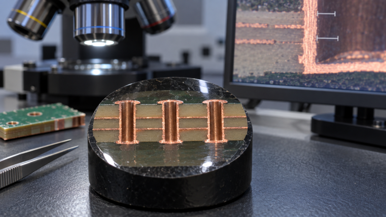
Figure 6: A polished microsection coupon under measurement after thermal stress
Measurement follows a defined pattern rather than a single reading. Wall thickness is recorded at several points around and along the barrel. That is because a single reading cannot distinguish a uniform 20 µm wall from a dog-bone averaging the same figure. The minimum value determines whether it's a pass or a fail.
| Requirement | Class 2 | Class 3 | Why It Changes Your Order |
|---|---|---|---|
| Average hole wall copper | 20 µm (787 µin) | 25 µm (984 µin) | Class 3 needs a longer plating cycle, so cost and lead time rise |
| Copper at the thinnest point | 18 µm (709 µin) | 20 µm (787 µin) | The thin point, not the average, is what cracks during reflow |
| Hole wall voids | One per hole, under 5% of length and 90 degrees of circumference, max 5% of holes | None permitted | Class 3 rejects boards. Class 2 would ship, so yield drops |
| Typical application | Industrial, consumer, and most commercial hardware | Aerospace, medical, and automotive safety systems | Specify Class 3 only where a field failure is genuinely unacceptable |
The second row is the one designers underestimate, since a barrel can average 22 µm and still carry a 12 µm patch that fails. Class 3 tightens the floor as well as the average, and that is where most of the extra process control goes.
FAQs about PCB Plating
Q: Does PCB plating change the finished board thickness?
Yes, though only slightly, and it happens on the outer layers rather than through the stackup. Electroplating adds roughly 20-25 µm of copper to the outer surfaces. A board ordered with 1 oz outer copper, therefore, finishes thicker than the foil alone.
Q: Why did my plated through hole fail after assembly instead of during electrical test?
Almost always a barrel crack that was closed at room temperature and opened under heat. A thin or uneven wall survives the fab's continuity test because both halves still touch.
Q: Does the surface finish add to a board's current-carrying capacity?
No, and it is safe to ignore it in your calculations. The layers are at most a few microns thick, and nickel conducts several times worse than copper, so the finish contributes almost nothing to conduction.
Q: Can I have hard gold edge fingers and ENIG pads on the same board?
Yes, and it is the normal way to build a card that plugs into a socket. Hard gold is selectively electroplated onto the contact fingers, while the rest of the board receives the cheaper finish.
Q: Do I need to specify IPC Class 3 to get reliable vias?
Usually not, because Class 2 already sets a 20 µm average hole wall and covers most industrial and consumer hardware comfortably. Class 3 raises the average to 25 µm and forbids hole wall voids entirely, which lowers yield and raises cost.
Conclusion
PCB plating is easy to treat as a fixed service the fab provides, but almost every variable in it is one you influence from the schematic. Hole size sets aspect ratio, copper weight sets bath time, feature pitch decides pattern versus panel plating, and the connector on your board decides the finish. None of those choices announces itself as a plating decision when you make them. The single habit worth building is to think in terms of the thinnest point rather than the average.
An average wall thickness passes reports, while the thin patch is what cracks after the fourth thermal cycle in the field. As boards get thinner and vias get smaller, that gap between average and minimum only widens. Microsection data is therefore worth reading rather than filing. JLCPCB's published plating specifications and IPC-compliant inspection make that data available on ordinary prototype orders, so you can check the assumption instead of trusting it.

Popular Articles
• Understanding the Basics of Electronic Devices and Circuits
• Understanding Digital Circuit Timing: Setup Time, Hold Time, Contamination Delay & Clock Skew
• PCBs Explained: A Simple Guide to Printed Circuit Boards
• Guide to the Top 10 Commonly Used Electronic Components
• Digital 101: Fundamental Building Blocks of Digital Logic Design
Keep Learning
Demystifying Bare PCB Quality for Reliability-Critical Applications
Key Takeaways Early Defect Catching: Catching faults at the bare board stage costs only the PCB, avoiding wasted components and rework later. Perfboard Risks: Zero PCBs lack reference planes and plated holes, causing signal noise above 10–20 MHz and pad lifting. Critical Material Specs: Reliability depends on hole barrel copper (20–25 µm), Tg, Td, and CTI ratings matching your operating environment. Finish & Shelf Life: HASL and ENIG last ~12 months, while OSP and Immersion Silver/Tin expire in ~6 mon......
A Comprehensive Guide to Capacitor ESR: What It Is, Good Values, and How to Measure It
Key Takeaways Definition: Capacitor ESR (equivalent series resistance) is the single resistance that represents the losses inside a real capacitor, from its electrodes, terminations, electrolyte, and dielectric. Why It Matters: Ripple current flowing through the ESR produces a ripple-voltage step on the supply rail and I²R heating in the capacitor, which limits the capacitor's ripple-current rating and service life. Conditions Matter: ESR varies with frequency, temperature, capacitance, case size, and......
Understanding IPC-6012 Standards for High-Reliability Rigid PCB Fabrication
Key Takeaways IPC-6012 vs. IPC-A-600: IPC-6012 is the binding specification, while IPC-A-600 is only for visual reference. Class 2 vs. Class 3: Class 3 requires thicker copper (25μm vs. 20μm) and zero plating voids. Coupon Verification: Quality is tested by microsectioning panel coupons after thermal stress. Upfront Callout: Specify the class on drawings upfront; boards cannot be upgraded later. IPC-6012 is the line on your fabrication drawing that decides what your supplier is allowed to ship. Most d......
Mastering PCB Plating Types and Process Control in High-Yield Fabrication
Key Takeaways Two-Step Plating: Chemical seed layer comes first, electrolytic copper adds structural strength. Process Choice: Pattern plating enables fine tracks; panel plating suits heavy copper. Via Integrity: Keep aspect ratio ≤ 10:1 to prevent thinnest-point barrel cracking. Surface Finishes: Use ENIG for flat BGA pads and hard gold for high-wear contacts. IPC Standards: Class 2 mandates 20μm copper wall thickness; Class 3 requires 25μm with zero voids. PCB plating turns a stack of drilled lamina......
Can PCB Autorouters Really Deliver Production-Ready Designs?
Key Takeaways Rules over DRC: A clean DRC only proves rules were followed, not that the board works. Placement First: Autorouters cannot compensate for bad component placement. Selective Automation: Hand-route power, analog, and high-speed traces; autoroute only repetitive or low-speed nets. DFM Validation: Verify real manufacturing tolerances before sending files to production. Every PCB autorouter sells the same promise: press one button and watch the ratlines turn into copper. On a simple two-layer......
Basic Bridge Circuits
Key Takeaways Core Principle: Bridge circuits (Wheatstone, Kelvin, H-Bridge, etc.) enable high-precision measurements and power control. Applications: Essential for sensor signal conditioning, AC/DC rectifiers, and motor drivers. JLCPCB Optimization: Maximize circuit stability with JLCPCB’s 3/3 mil traces, 4-layer stackups, and High-TG FR-4. A bridge circuit splits an input voltage into two paths, compares the voltages across different branches, and provides an output. These circuits are widely valued......